


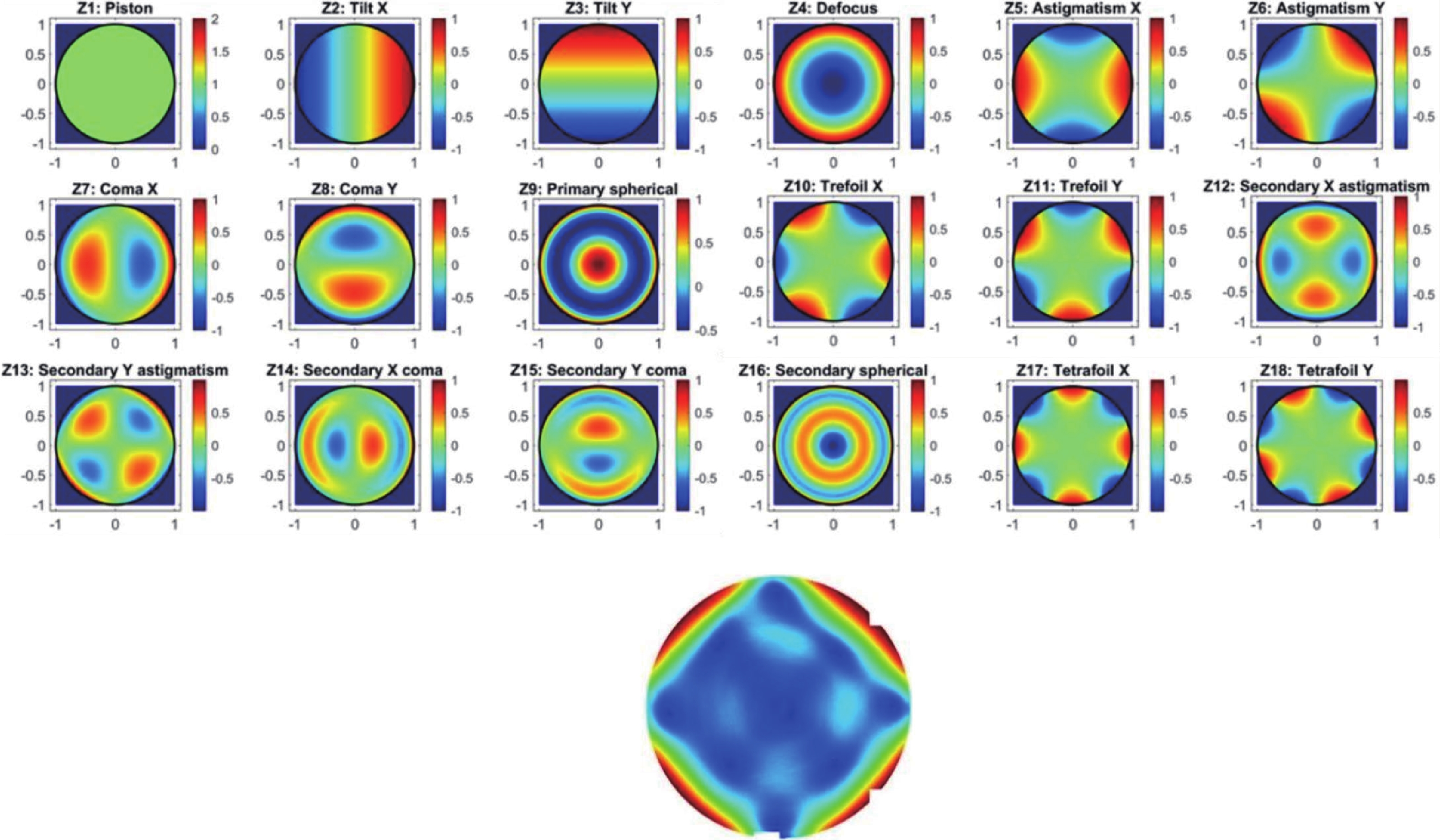
Fig. 1.
(Color online) Comparison of the first 18 Zernike polynomial wafer distribution maps and the characteristic post-bonding residual distribution for a (100) silicon wafer.
ARTICLES
Rui Wang1, Sen Lu1, 2, Kaiming Yang1, and Yu Zhu1, 2
Corresponding author: Kaiming Yang, yangkm@tsinghua.edu.cn
Abstract: To address the demand for sub-100-nm overlay accuracy in wafer bonding for 3D integration, this study proposes an extended overlay assessment model integrating physical mechanisms and data-driven approaches, along with a correlation analysis methodology with process parameters. Rigid-body models inadequately characterize systematic deformations from crystalline anisotropy and process stresses. To overcome this, we construct an extended overlay model based on Zernike polynomials, incorporating physically meaningful terms for precise description of non-uniform wafer deformation. An innovative Zernike term selection strategy combining physics-guided pre-screening and AIC-optimized stepwise regression resolves overfitting/underfitting, enhancing generalizability and interpretability. Validation using patterned wafer geometry (PWG) data shows the model achieves R² > 0.70 for both net bonding deformation and lithography-compensable components, demonstrating excellent deformation decomposition. Correlation analysis of multiple process experiments reveals strong correlations (|r| > 0.85) between key process parameters (e.g., peak bonding head force) and specific Zernike modes, providing evidence for suppressing detrimental deformations via process optimization. This research establishes a complete framework from theory to experimental verification and process traceability, laying a foundation for mechanism diagnosis, predictive compensation, and closed-loop control in high-precision wafer bonding.
Keywords: wafer bonding, overlay assessment, anisotropic deformation, Zernike polynomials, process correlation
| [1] |
Panigrahi A K, Bonam S, Ghosh T, et al. Low temperature, low pressure CMOS compatible Cu-Cu thermo-compression bonding with Ti passivation for 3D IC integration. 2015 IEEE 65th Electronic Components and Technology Conference (ECTC), 2015: 2205 doi: 10.1109/ECTC.2015.7159909
|
| [2] |
Mitsuishi H, Mori H, Maeda H, et al. 50 nm overlay accuracy for wafer-to-wafer bonding by high-precision alignment technologies. 2023 IEEE 73rd Electronic Components and Technology Conference (ECTC), 2023: 1664 doi: 10.1109/ECTC51909.2023.00283
|
| [3] |
Rebhan B, Bernauer M, Wagenleitner T, et al. 200 nm wafer-to-wafer overlay accuracy in wafer level Cu/SiO2 hybrid bonding for BSI CIS. 2015 IEEE 17th Electronics Packaging and Technology Conference (EPTC), 2015: 1 doi: 10.1109/EPTC.2015.7412403
|
| [4] |
McNally P J. B-Spline X-Ray diffraction imaging techniques for die warpage and stress monitoring inside fully encapsulated packaged chips. 2015 16th International Conference on Thermal, Mechanical and Multi-Physics Simulation and Experiments in Microelectronics and Microsystems, 2015: 1 doi: 10.1109/EuroSimE.2015.7103166
|
| [5] |
van Dijk L, Mileham J, Malakhovsky I, et al. Wafer-shape based in-plane distortion predictions using superfast 4G metrology. Metrol Insp Process Control Microlithogr XXXI, 2017, 10145: 101452L doi: 10.1117/12.2257475
|
| [6] |
Das H, Sunkari S, Justice J, et al. Detection of dislocations using X-ray diffraction imaging (topography) KOH etching and their evolution after epitaxial growth in 4H-SiC. ECS Trans, 2021, 104(7): 141 doi: 10.1149/ma2021-02341005mtgabs
|
| [7] |
Savchuk O, Volinsky A A. Nonparametric estimation of SiC film residual stress from the wafer surface profile. Measurement, 2021, 177: 109238 doi: 10.1016/j.measurement.2021.109238
|
| [8] |
Dedkova A A, Florinsky I V, Djuzhev N A. Approaches to determining curvature of wafers by their topography. Phys Usp, 2022, 65: 706 doi: 10.3367/ufnr.2021.10.039076
|
| [9] |
Chen X W, Yue W V. Residual stress concentration due to nano-scaled particulate contamination at direct bonding interface with localized material inhomogeneity. J Elast, 2024, 156(4): 1121 doi: 10.1007/s10659-024-10089-2
|
| [10] |
Tseng M L, Gorji N E. Metrology of warpage in silicon wafers using X-ray diffraction mapping. IEEE Trans Compon, Packag Manuf Technol, 2025, 15(7): 1523 doi: 10.1109/TCPMT.2025.3557270
|
| [11] |
Zhang X D, Han Z G, Zhao L, et al. Optimized characterization model of curvature radius-stress for wafer thin films. Acta Opt Sin, 2025, 45(16): 1612001 doi: 10.3788/AOS250950
|
| [12] |
Ju J, Kim M, Lee J, et al. Application of overlay modeling and control with Zernike polynomials in an HVM environment. Metrol Insp Process Control Microlithogr XXX, 2016, 9778: 977825 doi: 10.1117/12.2219739
|
| [13] |
Zhang L B, Feng Y B, Song Z, et al. Zernike model for overlay control and tool monitor for lithography and etch process. J Vac Sci Technol B, 2022, 40(6): 062604 doi: 10.1116/6.0002239
|
| [14] |
Duclaux B, Boustheen A, Pastol A, et al. Overcoming challenges raised by wafer load grid overlay fingerprints and correction per exposure management. Metrology, Inspection, and Process Control XXXIX, 2025: 110 doi: 10.1117/12.3050691
|
| [15] |
Ohri A, Taylor T L, Temchenko V, et al. Zernike-based photolithography track modules matching for wafer CDU. Metrology, Inspection, and Process Control XXXIX, 2025: 37 doi: 10.1117/12.3051932
|
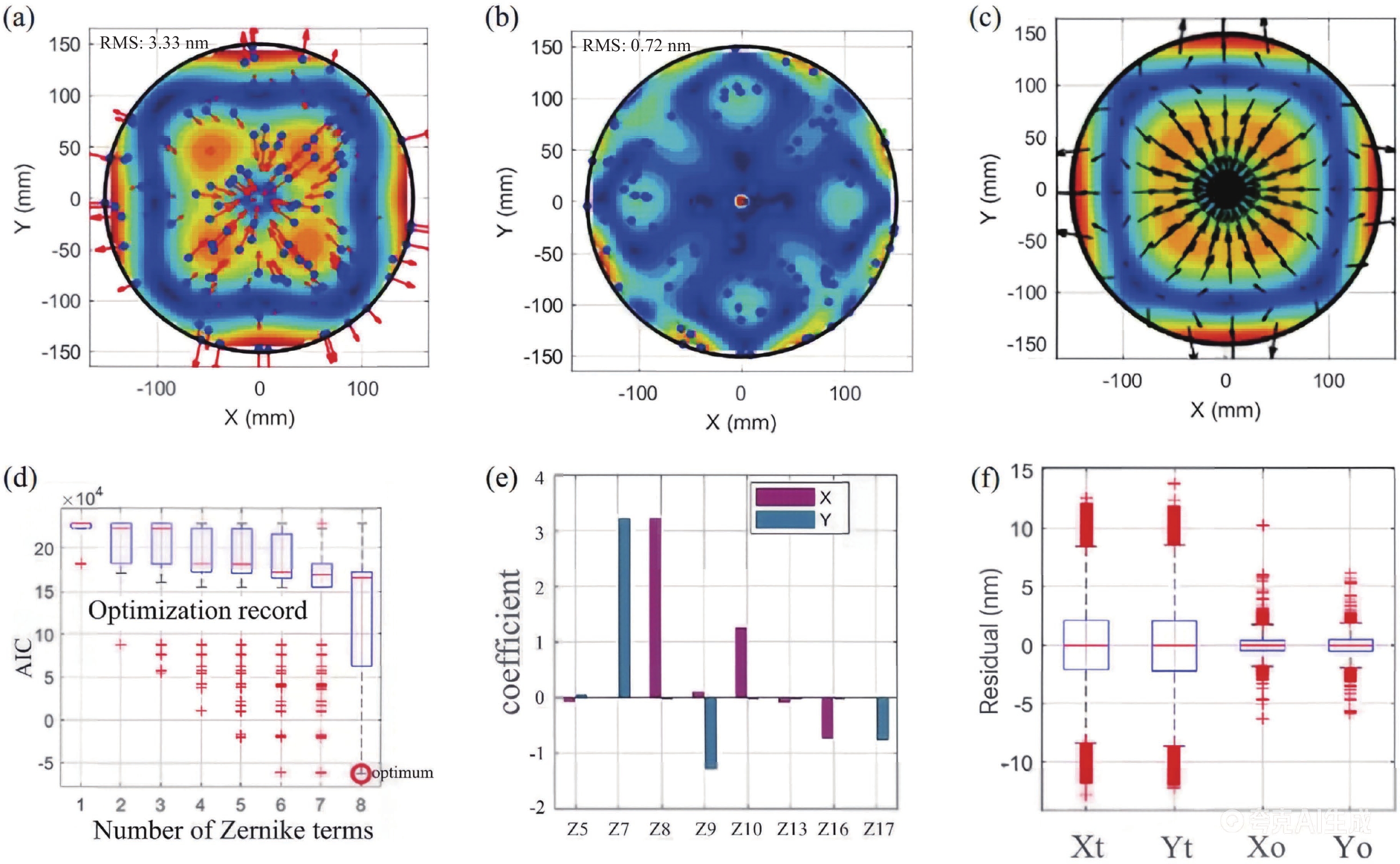
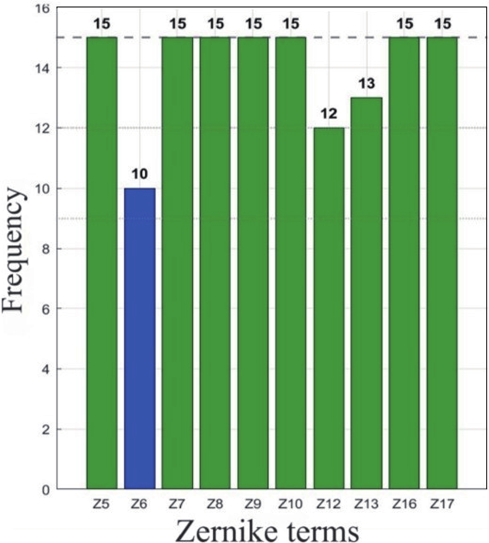
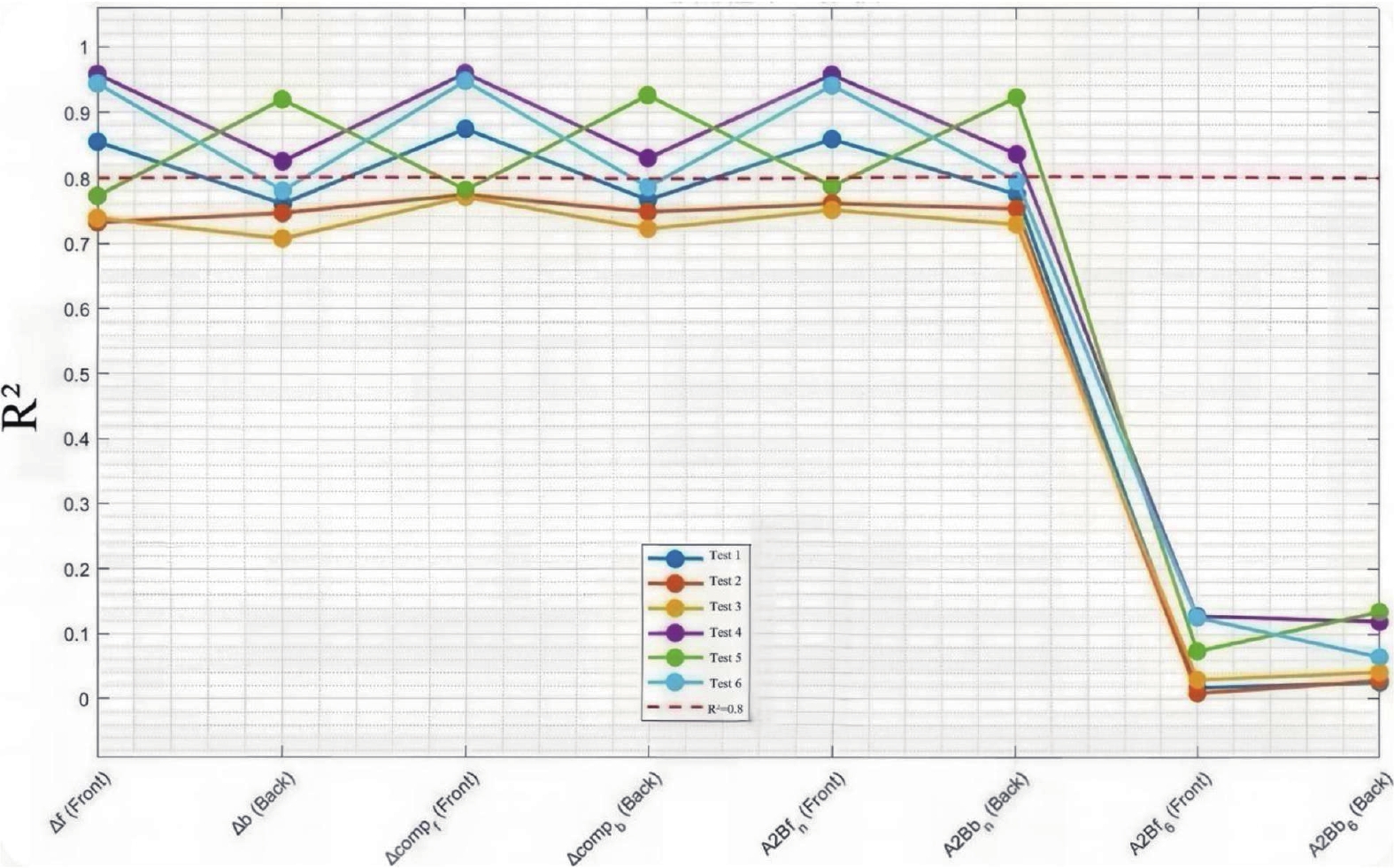
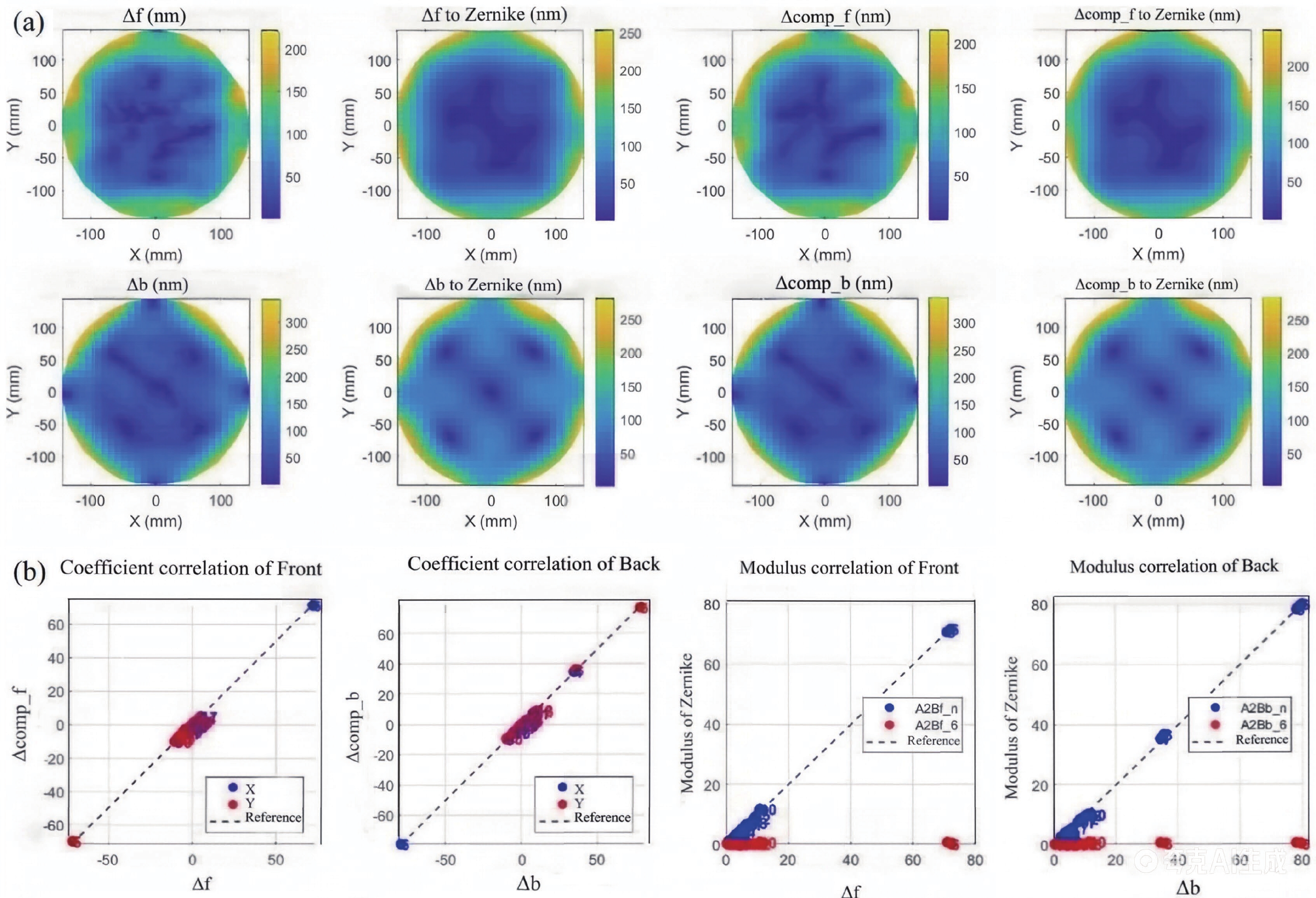
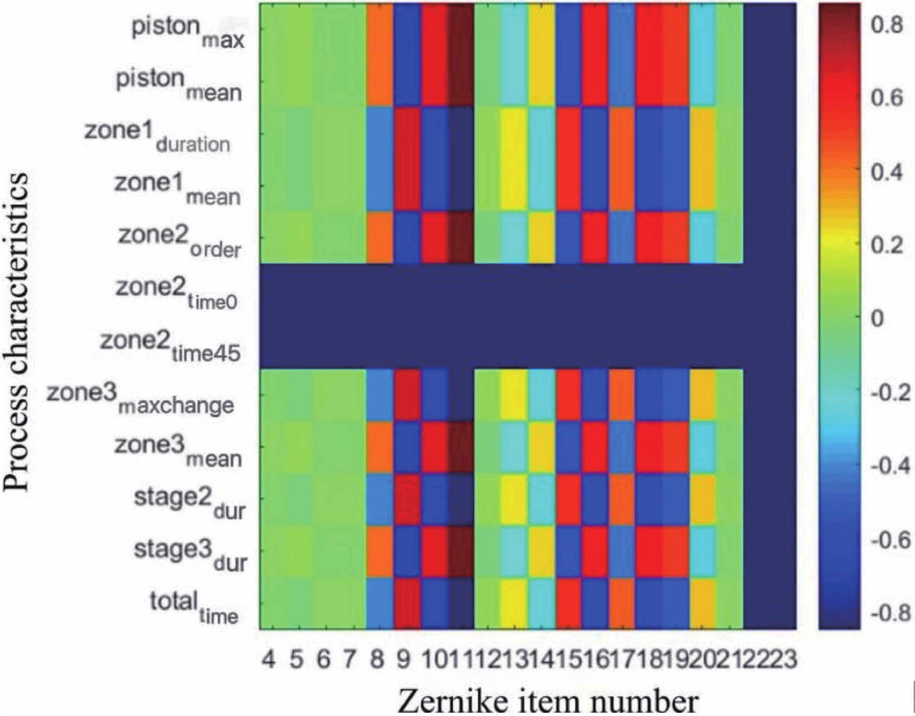
Table 1. Comparison of fitting results for the three zernike models.
| Model | Selected terms | k | Residual RMS (nm) | RMSE_CV (nm) | AIC |
| Traditional full-term | Z1−Z30 | 30 | 0.58 | 1.21 | −707911 |
| Empirical-term | Z5, Z6, Z17, Z18 | 4 | 3.32 | 3.57 | −542216 |
| Optimally selected | Z5, Z7, Z8, Z9, Z10, Z13, Z16, Z17 | 8 | 0.88 | 0.91 | −668943 |
 DownLoad: CSV
Table 2. Comprehensive performance comparison of the three overlay extension models across multiple wafers.
| Model | Fitted residual RMS (nm) | Average cross-validation RMSE (nm) | RMSE_CV standard deviation (nm) | Average AIC | Single-pair fitting time (s) |
| Traditional full-term | 0.62 | 1.19 | 0.24 | −712333 | 12.5 |
| Empirical-term | 3.18 | 3.55 | 0.38 | −523879 | 0.8 |
| Optimally selected | 0.83 | 0.93 | 0.12 | −687631 | 5.2 |
DownLoad: CSV
Table 3. Correlation coefficient matrix between key process features and Zernike coefficients (partial). Each cell shows the Pearson correlation coefficient r with the corresponding p-value in parentheses.
| Process feature | Z8 | Z9 | Z10 | Z11 | Z15 | Z16 | Z18 | Z19 |
| Peak bonding head force | 0.401 (0.088) |
−0.684 (0.002) |
0.640 (0.004) |
0.852 (<0.001) |
−0.553 (0.017) |
0.589 (0.010) |
0.620 (0.006) |
0.517 (0.025) |
| Zone_1 pressure hold time | −0.401 (0.088) |
0.684 (0.002) |
−0.640 (0.004) |
−0.852 (<0.001) |
0.553 (0.017) |
−0.589 (0.010) |
−0.620 (0.006) |
−0.517 (0.025) |
| Max. change rate of Zone_3 pressure | −0.401 (0.088) |
0.684 (0.002) |
−0.640 (0.004) |
−0.852 (<0.001) |
0.553 (0.017) |
−0.589 (0.010) |
−0.620 (0.006) |
−0.517 (0.025) |
DownLoad: CSV
Table 4. Correlation coefficients between process features and deformation symmetry groups.
| Process feature | Rotational symmetry | Four-fold symmetry | Eight-fold symmetry |
| Peak bonding head force | 0.009 | −0.064 | −0.268 |
| Zone_1 pressure hold time | −0.009 | 0.064 | 0.268 |
| Zone_3 average pressure | 0.009 | −0.064 | −0.268 |
DownLoad: CSV
| [1] |
Panigrahi A K, Bonam S, Ghosh T, et al. Low temperature, low pressure CMOS compatible Cu-Cu thermo-compression bonding with Ti passivation for 3D IC integration. 2015 IEEE 65th Electronic Components and Technology Conference (ECTC), 2015: 2205 doi: 10.1109/ECTC.2015.7159909
|
| [2] |
Mitsuishi H, Mori H, Maeda H, et al. 50 nm overlay accuracy for wafer-to-wafer bonding by high-precision alignment technologies. 2023 IEEE 73rd Electronic Components and Technology Conference (ECTC), 2023: 1664 doi: 10.1109/ECTC51909.2023.00283
|
| [3] |
Rebhan B, Bernauer M, Wagenleitner T, et al. 200 nm wafer-to-wafer overlay accuracy in wafer level Cu/SiO2 hybrid bonding for BSI CIS. 2015 IEEE 17th Electronics Packaging and Technology Conference (EPTC), 2015: 1 doi: 10.1109/EPTC.2015.7412403
|
| [4] |
McNally P J. B-Spline X-Ray diffraction imaging techniques for die warpage and stress monitoring inside fully encapsulated packaged chips. 2015 16th International Conference on Thermal, Mechanical and Multi-Physics Simulation and Experiments in Microelectronics and Microsystems, 2015: 1 doi: 10.1109/EuroSimE.2015.7103166
|
| [5] |
van Dijk L, Mileham J, Malakhovsky I, et al. Wafer-shape based in-plane distortion predictions using superfast 4G metrology. Metrol Insp Process Control Microlithogr XXXI, 2017, 10145: 101452L doi: 10.1117/12.2257475
|
| [6] |
Das H, Sunkari S, Justice J, et al. Detection of dislocations using X-ray diffraction imaging (topography) KOH etching and their evolution after epitaxial growth in 4H-SiC. ECS Trans, 2021, 104(7): 141 doi: 10.1149/ma2021-02341005mtgabs
|
| [7] |
Savchuk O, Volinsky A A. Nonparametric estimation of SiC film residual stress from the wafer surface profile. Measurement, 2021, 177: 109238 doi: 10.1016/j.measurement.2021.109238
|
| [8] |
Dedkova A A, Florinsky I V, Djuzhev N A. Approaches to determining curvature of wafers by their topography. Phys Usp, 2022, 65: 706 doi: 10.3367/ufnr.2021.10.039076
|
| [9] |
Chen X W, Yue W V. Residual stress concentration due to nano-scaled particulate contamination at direct bonding interface with localized material inhomogeneity. J Elast, 2024, 156(4): 1121 doi: 10.1007/s10659-024-10089-2
|
| [10] |
Tseng M L, Gorji N E. Metrology of warpage in silicon wafers using X-ray diffraction mapping. IEEE Trans Compon, Packag Manuf Technol, 2025, 15(7): 1523 doi: 10.1109/TCPMT.2025.3557270
|
| [11] |
Zhang X D, Han Z G, Zhao L, et al. Optimized characterization model of curvature radius-stress for wafer thin films. Acta Opt Sin, 2025, 45(16): 1612001 doi: 10.3788/AOS250950
|
| [12] |
Ju J, Kim M, Lee J, et al. Application of overlay modeling and control with Zernike polynomials in an HVM environment. Metrol Insp Process Control Microlithogr XXX, 2016, 9778: 977825 doi: 10.1117/12.2219739
|
| [13] |
Zhang L B, Feng Y B, Song Z, et al. Zernike model for overlay control and tool monitor for lithography and etch process. J Vac Sci Technol B, 2022, 40(6): 062604 doi: 10.1116/6.0002239
|
| [14] |
Duclaux B, Boustheen A, Pastol A, et al. Overcoming challenges raised by wafer load grid overlay fingerprints and correction per exposure management. Metrology, Inspection, and Process Control XXXIX, 2025: 110 doi: 10.1117/12.3050691
|
| [15] |
Ohri A, Taylor T L, Temchenko V, et al. Zernike-based photolithography track modules matching for wafer CDU. Metrology, Inspection, and Process Control XXXIX, 2025: 37 doi: 10.1117/12.3051932
|


Article views: 1080 Times PDF downloads: 227 Times Cited by: 0 Times
Received: 20 December 2025 Revised: 21 January 2026 Online: Accepted Manuscript: 02 March 2026Uncorrected proof: 06 March 2026Published: 14 May 2026
| Citation: |
Rui Wang, Sen Lu, Kaiming Yang, Yu Zhu. An extended overlay assessment model with process correlation analysis for sub-100-nm accuracy wafer bonding[J]. Journal of Semiconductors, 2026, 47(5): 052303. doi: 10.1088/1674-4926/25120038
****
R Wang, S Lu, K M Yang, and Y Zhu, An extended overlay assessment model with process correlation analysis for sub-100-nm accuracy wafer bonding[J]. J. Semicond., 2026, 47(5): 052303 doi: 10.1088/1674-4926/25120038

|
 Rui Wang is studying for a Ph.D. in Mechanical Engineering in Tsinghua University. He received his BS degree in Mechanical Engineering from Tsinghua University in 2019. His main research direction is Accuracy Guarantee of Alignment and Bonding technology for wafer stacking equipment
 Sen Lu is an assistant professor at the Department of Mechanical Engineering at Tsinghua University. He received his PhD in mechanical engineering from Tsinghua University in 2019. His current interests include ultra-precision measurement and control technology as well as 3D IC packaging technology
 Kaiming Yang is a professor at the Department of Mechanical Engineering at Tsinghua University. He received his BS and MS degrees in Mechanical Engineering from Zhengzhou University in 1995 and 1998, respectively, and his PhD in Mechanical Manufacturing and Automation from Tsinghua University in 2005. His research areas include ultra-precision motion control, computerized numerical control, and mechatronic equipment control
 Yu Zhu graduated from the China University of Mining and Technology in 2001 with a doctoral degree. From July 2001 to September 2004, he worked as a postdoctoral fellow at Tsinghua University. He is the head of the Institute of Mechanical Electronics at the Department of Mechanical Engineering at Tsinghua University and a leader in the field of IC equipment at Tsinghua University. His research interests include dynamical system design and analysis theory for ultra-precision systems, displacement measurement and motion control technology for nano-precision systems, and development strategies for IC manufacturing equipment
| [1] |
Panigrahi A K, Bonam S, Ghosh T, et al. Low temperature, low pressure CMOS compatible Cu-Cu thermo-compression bonding with Ti passivation for 3D IC integration. 2015 IEEE 65th Electronic Components and Technology Conference (ECTC), 2015: 2205 doi: 10.1109/ECTC.2015.7159909
|
| [2] |
Mitsuishi H, Mori H, Maeda H, et al. 50 nm overlay accuracy for wafer-to-wafer bonding by high-precision alignment technologies. 2023 IEEE 73rd Electronic Components and Technology Conference (ECTC), 2023: 1664 doi: 10.1109/ECTC51909.2023.00283
|
| [3] |
Rebhan B, Bernauer M, Wagenleitner T, et al. 200 nm wafer-to-wafer overlay accuracy in wafer level Cu/SiO2 hybrid bonding for BSI CIS. 2015 IEEE 17th Electronics Packaging and Technology Conference (EPTC), 2015: 1 doi: 10.1109/EPTC.2015.7412403
|
| [4] |
McNally P J. B-Spline X-Ray diffraction imaging techniques for die warpage and stress monitoring inside fully encapsulated packaged chips. 2015 16th International Conference on Thermal, Mechanical and Multi-Physics Simulation and Experiments in Microelectronics and Microsystems, 2015: 1 doi: 10.1109/EuroSimE.2015.7103166
|
| [5] |
van Dijk L, Mileham J, Malakhovsky I, et al. Wafer-shape based in-plane distortion predictions using superfast 4G metrology. Metrol Insp Process Control Microlithogr XXXI, 2017, 10145: 101452L doi: 10.1117/12.2257475
|
| [6] |
Das H, Sunkari S, Justice J, et al. Detection of dislocations using X-ray diffraction imaging (topography) KOH etching and their evolution after epitaxial growth in 4H-SiC. ECS Trans, 2021, 104(7): 141 doi: 10.1149/ma2021-02341005mtgabs
|
| [7] |
Savchuk O, Volinsky A A. Nonparametric estimation of SiC film residual stress from the wafer surface profile. Measurement, 2021, 177: 109238 doi: 10.1016/j.measurement.2021.109238
|
| [8] |
Dedkova A A, Florinsky I V, Djuzhev N A. Approaches to determining curvature of wafers by their topography. Phys Usp, 2022, 65: 706 doi: 10.3367/ufnr.2021.10.039076
|
| [9] |
Chen X W, Yue W V. Residual stress concentration due to nano-scaled particulate contamination at direct bonding interface with localized material inhomogeneity. J Elast, 2024, 156(4): 1121 doi: 10.1007/s10659-024-10089-2
|
| [10] |
Tseng M L, Gorji N E. Metrology of warpage in silicon wafers using X-ray diffraction mapping. IEEE Trans Compon, Packag Manuf Technol, 2025, 15(7): 1523 doi: 10.1109/TCPMT.2025.3557270
|
| [11] |
Zhang X D, Han Z G, Zhao L, et al. Optimized characterization model of curvature radius-stress for wafer thin films. Acta Opt Sin, 2025, 45(16): 1612001 doi: 10.3788/AOS250950
|
| [12] |
Ju J, Kim M, Lee J, et al. Application of overlay modeling and control with Zernike polynomials in an HVM environment. Metrol Insp Process Control Microlithogr XXX, 2016, 9778: 977825 doi: 10.1117/12.2219739
|
| [13] |
Zhang L B, Feng Y B, Song Z, et al. Zernike model for overlay control and tool monitor for lithography and etch process. J Vac Sci Technol B, 2022, 40(6): 062604 doi: 10.1116/6.0002239
|
| [14] |
Duclaux B, Boustheen A, Pastol A, et al. Overcoming challenges raised by wafer load grid overlay fingerprints and correction per exposure management. Metrology, Inspection, and Process Control XXXIX, 2025: 110 doi: 10.1117/12.3050691
|
| [15] |
Ohri A, Taylor T L, Temchenko V, et al. Zernike-based photolithography track modules matching for wafer CDU. Metrology, Inspection, and Process Control XXXIX, 2025: 37 doi: 10.1117/12.3051932
|

 WeChat ID
Journal of Semiconductors © 2017 All Rights Reserved 京ICP备05085259号-2


