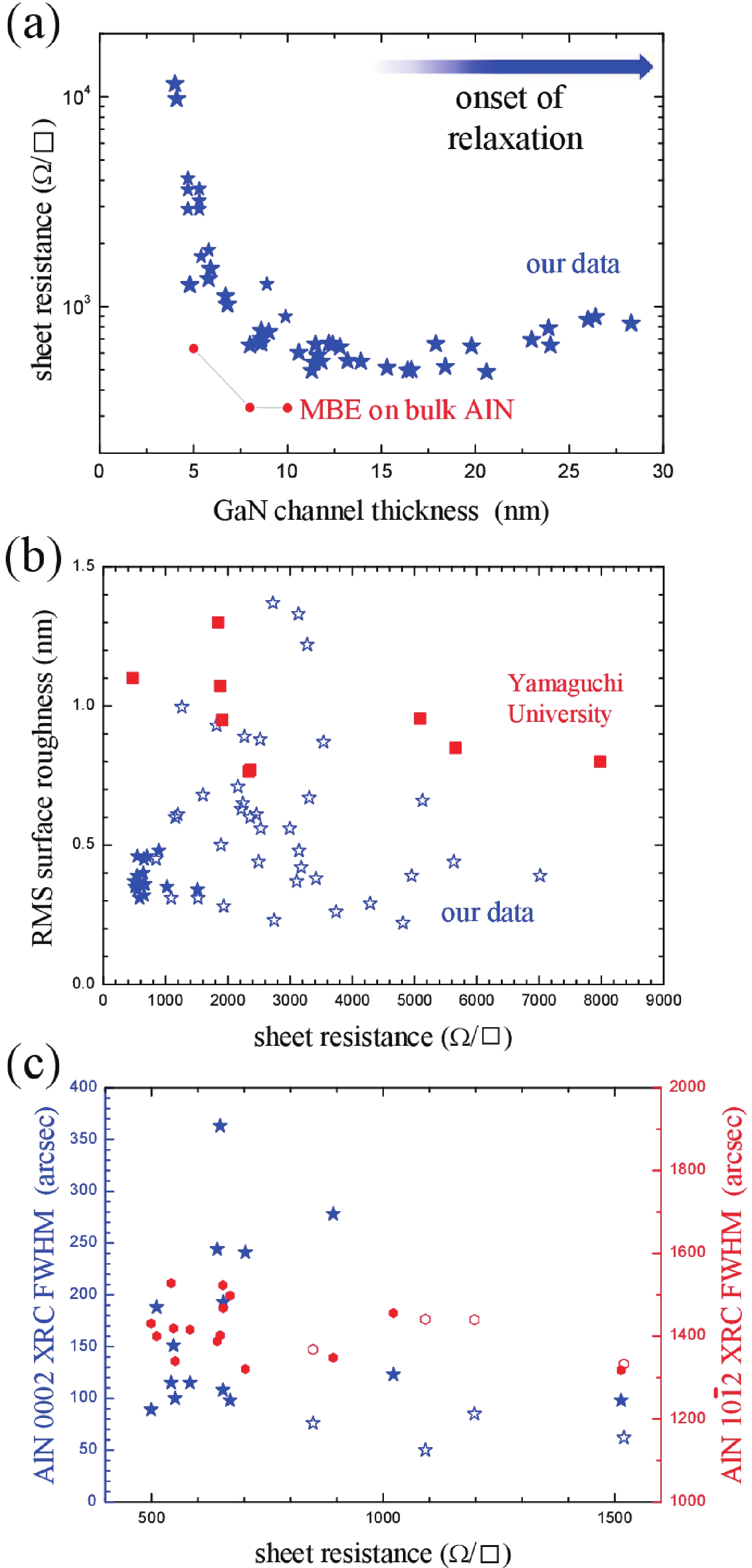
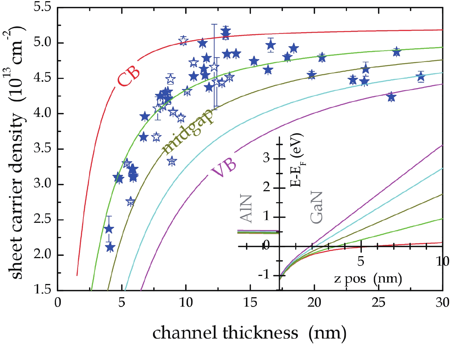
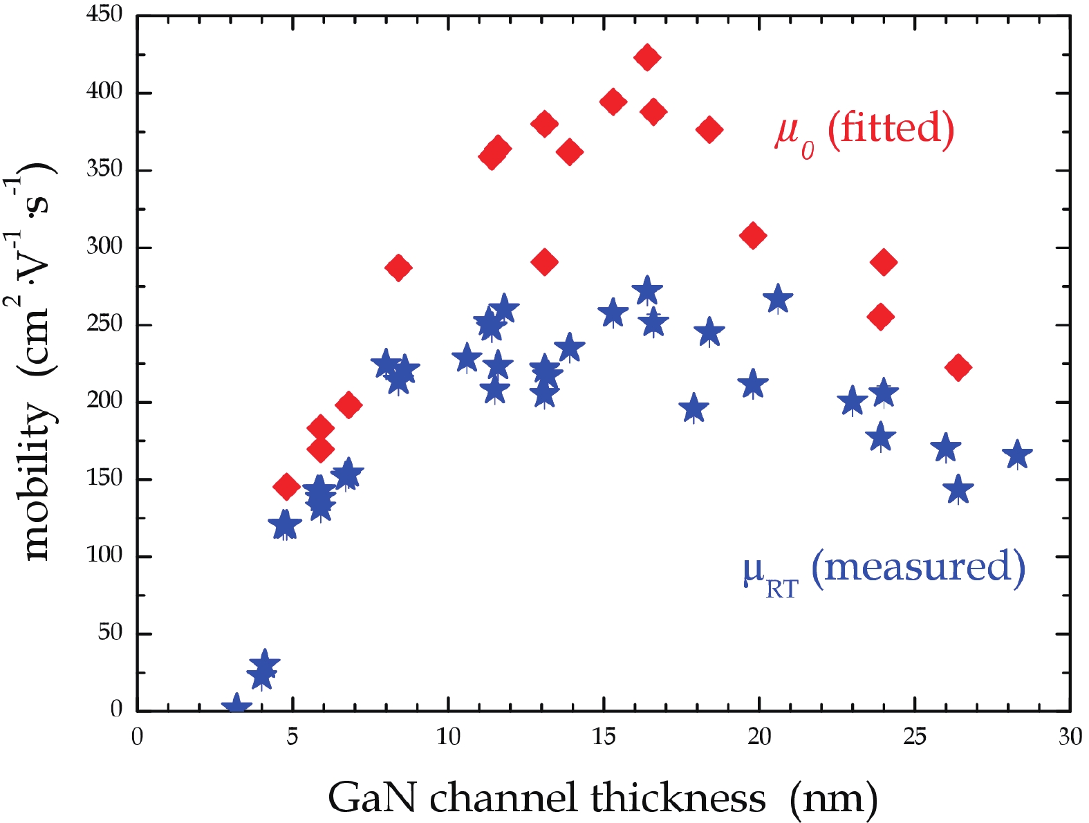
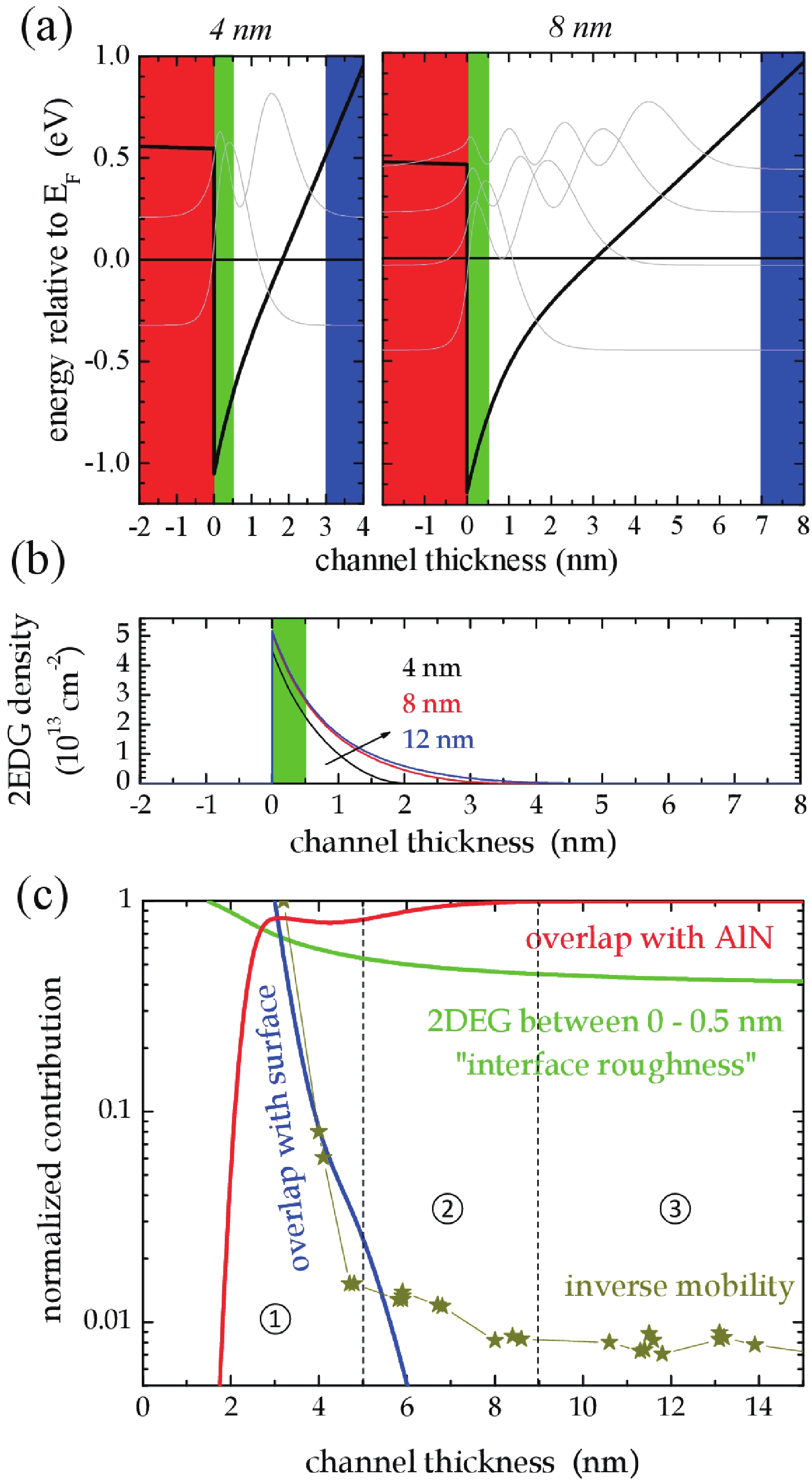
| [1] |
Ambacher O, Foutz B, Smart J, et al. Two dimensional electron gases induced by spontaneous and piezoelectric polarization in undoped and doped AlGaN/GaN heterostructures. J Appl Phys, 2000, 87(1): 334 doi: 10.1063/1.371866 |
| [2] |
Xie J, Mita S, Collazo R, et al. The effect of N-polar GaN domains as Ohmic contacts. Appl Phys Lett, 2010, 97(12): 123502 doi: 10.1063/1.3491173 |
| [3] |
Wong M H, Keller S, Dasgupta N S, et al. N-polar GaN epitaxy and high electron mobility transistors. Semicond Sci Technol, 2013, 28(7): 074009 doi: 10.1088/0268-1242/28/7/074009 |
| [4] |
Kim E, Zhang Z X, Singhal J, et al. First demonstration of N-polar GaN/AlGaN/AlN HEMT on single crystal AlN substrates. 2022 Device Research Conference (DRC), 2022: 1 doi: 10.1109/drc55272.2022.9855776 |
| [5] |
Kim E, Zhang Z X, Encomendero J, et al. N-polar GaN/AlGaN/AlN high electron mobility transistors on single-crystal bulk AlN substrates. Appl Phys Lett, 2023, 122(9): 092104 doi: 10.1063/5.0138939 |
| [6] |
Zazuli A H, Kowaki T, Miyamoto M, et al. Electrical properties of N-polar GaN/AlGaN/AlN grown via metal-organic vapor phase epitaxy. Phys Status Solidi A, 2024, 221(21): 2400060 doi: 10.1002/pssa.202400060 |
| [7] |
Kowaki T, Hanasaku K, Miyamoto M, et al. Effect of the twist crystallinity of N-polar AlN underlayer on the electrical properties of GaN/AlN structures. Phys Status Solidi A, 2024, 221(21): 2400053 doi: 10.1002/pssa.202400053 |
| [8] |
Yoshikawa A, Nagatomi T, Nagase K, et al. Pseudomorphic growth of a thin-GaN layer on the AlN single-crystal substrate using metal organic vapor phase epitaxy. Jpn J Appl Phys, 2024, 63(6): 060903 doi: 10.35848/1347-4065/ad565a |
| [9] |
Zhang C Z, Yin Y D, Huang P, et al. N-polar AlN-based enhancement-mode transistor with p-NiOx gate stacks and reduced buffer trapping. J Phys D Appl Phys, 2025, 58(48): 485104 doi: 10.1088/1361-6463/ae161c |
| [10] |
Furuhashi I, Pristovsek M, Yang X. N-polar GaN/AlN heterostructures on sapphire grown by metal-organic vapor phase epitaxy. J Crystal Growth, to be submitted
|
| [11] |
Pristovsek M, Furuhashi I, Yang X, et al. Two-dimensional electron gas in thin N-polar GaN channels on AlN on sapphire templates. Crystals, 2024, 14(9): 822 doi: 10.3390/cryst14090822 |
| [12] |
Pampili P, Pristovsek M. Nitrogen-polar growth of AlN on vicinal (0001) sapphire by MOVPE. J Appl Phys, 2024, 135(19): 195303 doi: 10.1063/5.0202746 |
| [13] |
tibercad simulation package, 2024. http://www.tibercad.org/
|
| [14] |
Dreyer C E, Janotti A, Van de Walle C G, et al. Correct implementation of polarization constants in wurtzite materials and impact on III-nitrides. Phys Rev X, 2016, 6(2): 021038 doi: 10.1103/physrevx.6.021038 |
| [15] |
Zazuli A H, Kowaki T, Miyamoto M, et al. Impact of thick N-polar AlN growth on crystalline quality and electrical properties of N-polar GaN/AlGaN/AlN FET. Jpn J Appl Phys, 2024, 63(9): 09SP11 doi: 10.35848/1347-4065/ad6e8f |
| [16] |
Miyamura M, Tachibana K, Arakawa Y. High-density and size-controlled GaN self-assembled quantum dots grown by metalorganic chemical vapor deposition. Appl Phys Lett, 2002, 80(21): 3937 doi: 10.1063/1.1482416 |
| [17] |
Simeonov D, Feltin E, Carlin J F, et al. Stranski-Krastanov GaN∕AlN quantum dots grown by metal organic vapor phase epitaxy. J Appl Phys, 2006, 99(8): 083509 doi: 10.1063/1.2189975 |
| [18] |
Weinstein I A, Vokhmintsev A S, Spiridonov D M. Thermoluminescence kinetics of oxygen-related centers in AlN single crystals. Diam Relat Mater, 2012, 25: 59 doi: 10.1016/j.diamond.2012.02.004 |
| [19] |
Wang H, Chen A B. Calculation of shallow donor levels in GaN. J Appl Phys, 2000, 87(11): 7859 doi: 10.1063/1.373467 |
| [20] |
Chung B C, Gershenzon M. The influence of oxygen on the electrical and optical properties of GaN crystals grown by metalorganic vapor phase epitaxy. J Appl Phys, 1992, 72(2): 651 doi: 10.1063/1.351848 |
| [21] |
Pristovsek M, Furuhashi I, Pampili P. Growth of N-polar (0001) GaN in metal–organic vapour phase epitaxy on sapphire. Crystals, 2023, 13(7): 1072 doi: 10.3390/cryst13071072 |
| [22] |
Reddy P, Bryan I, Bryan Z, et al. The effect of polarity and surface states on the Fermi level at III-nitride surfaces. J Appl Phys, 2014, 116(12): 123701 doi: 10.1063/1.4896377 |
| [23] |
Bartoš I, Romanyuk O, Houdkova J, et al. Electron band bending of polar, semipolar and non-polar GaN surfaces. J Appl Phys, 2016, 119(10): 105303 doi: 10.1063/1.4943592 |
| [24] |
Jana R K, Jena D. Stark-effect scattering in rough quantum wells. Appl Phys Lett, 2011, 99: 012104 doi: 10.1063/1.3607485 |
| [25] |
Singisetti U, Hoi Wong M, Mishra U K. Interface roughness scattering in ultra-thin N-polar GaN quantum well channels. Appl Phys Lett, 2012, 101: 012101 doi: 10.1063/1.4732795 |
| [26] |
Chen Y H, Encomendero J, Savant C, et al. Electron mobility enhancement by electric field engineering of AlN/GaN/AlN quantum-well HEMTs on single-crystal AlN substrates. Appl Phys Lett, 2024, 124(15): 152111 doi: 10.1063/5.0190822 |
| [27] |
Zhang Z X, Encomendero J, Kim E, et al. High-density polarization-induced 2D electron gases in N-polar pseudomorphic undoped GaN/Al 0.85Ga 0.15N heterostructures on single-crystal AlN substrates. Appl Phys Lett, 2022, 121(8): 082107 doi: 10.1063/5.0107159 |
| [28] |
Vurgaftman I, Meyer J R. Band parameters for nitrogen-containing semiconductors. J Appl Phys, 2003, 94(6): 3675 doi: 10.1063/1.1600519 |
| [29] |
Vurgaftman I, Meyer J R, Ram-Mohan L R. Band parameters for III–V compound semiconductors and their alloys. J Appl Phys, 2001, 89(11): 5815 doi: 10.1063/1.1368156 |
| [30] |
Gaska R, Shur M S, Bykhovski A D. Pyroelectric and piezoelectric properties of GaN-based materials. MRS Internet J Nitride Semicond Res, 1999, 4(1): 57 doi: 10.1557/S1092578300002246 |
| [31] |
Feneberg M, Thonke K. Polarization fields of III-nitrides grown in different crystal orientations. J Phys Condens Matter, 2007, 19(40): 403201 doi: 10.1088/0953-8984/19/40/403201 |
| [32] |
Nakamura N, Ogi H, Hirao M. Elastic, anelastic, and piezoelectric coefficients of GaN. J Appl Phys, 2012, 111: 013509 doi: 10.1063/1.3674271 |
| [33] |
Sedhain A, Li J, Lin J Y, et al. Probing exciton-phonon interaction in AlN epilayers by photoluminescence. Appl Phys Lett, 2009, 95(6): 061106 doi: 10.1063/1.3206672 |
| [34] |
Ilegems M, Dingle R, Logan R A. Luminescence of Zn- and Cd-doped GaN. J Appl Phys, 1972, 43(9): 3797 doi: 10.1063/1.1661813 |
| [35] |
Goldhahn R. Dielectric function of nitride semiconductors: Recent experimental results. Acta Phys Pol A, 2003, 104(2): 123 doi: 10.12693/aphyspola.104.123 |
| [36] |
Shokhovets S, Goldhahn R, Gobsch G, et al. Determination of the anisotropic dielectric function for wurtzite AlN and GaN by spectroscopic ellipsometry. J Appl Phys, 2003, 94(1): 307 doi: 10.1063/1.1582369 |
| [37] |
Akasaki I, Hashimoto M. Infrared lattice vibration of vapour-grown AlN. Solid State Commun, 1967, 5(11): 851 doi: 10.1016/0038-1098(67)90313-4 |
| [38] |
Barker A S, Ilegems M. Infrared lattice vibrations and free-electron dispersion in GaN. Phys Rev B, 1973, 7(2): 743 doi: 10.1103/PhysRevB.7.743 |
| [39] |
Yan Q M, Rinke P, Scheffler M, et al. Strain effects in group-III nitrides: Deformation potentials for AlN, GaN, and InN. Appl Phys Lett, 2009, 95(12): 121111 doi: 10.1063/1.3236533 |
| [40] |
Shur M, Gelmont B, Asif Khan M. Electron mobility in two-dimensional electron gas in AIGaN/GaN heterostructures and in bulk GaN. J Electron Mater, 1996, 25(5): 777 doi: 10.1007/BF02666636 |
| [41] |
Zanato D, Gokden S, Balkan N, et al. The effect of interface-roughness and dislocation scattering on low temperature mobility of 2D electron gas in GaN/AlGaN. Semicond Sci Technol, 2004, 19(3): 427 doi: 10.1088/0268-1242/19/3/024 |
| [42] |
Gurusinghe M N, Davidsson S K, Andersson T G. Two-dimensional electron mobility limitation mechanisms in Al xGa 1–xN/GaN heterostructures. Phys Rev B, 2005, 72(4): 045316 doi: 10.1103/physrevb.72.045316 |
| [43] |
Alause H, Knap W, Azema S C, et al. Optical and electrical properties of 2-dimensional electron gas in GaN/AlGaN heterostructures. Mater Sci Eng B, 1997, 46(1/2/3): 79 doi: 10.1016/s0921-5107(96)01936-8 |
| [44] |
Knap W, Contreras S, Alause H, et al. Cyclotron resonance and quantum Hall effect studies of the two-dimensional electron gas confined at the GaN/AlGaN interface. Appl Phys Lett, 1997, 70(16): 2123 doi: 10.1063/1.118967 |
| [45] |
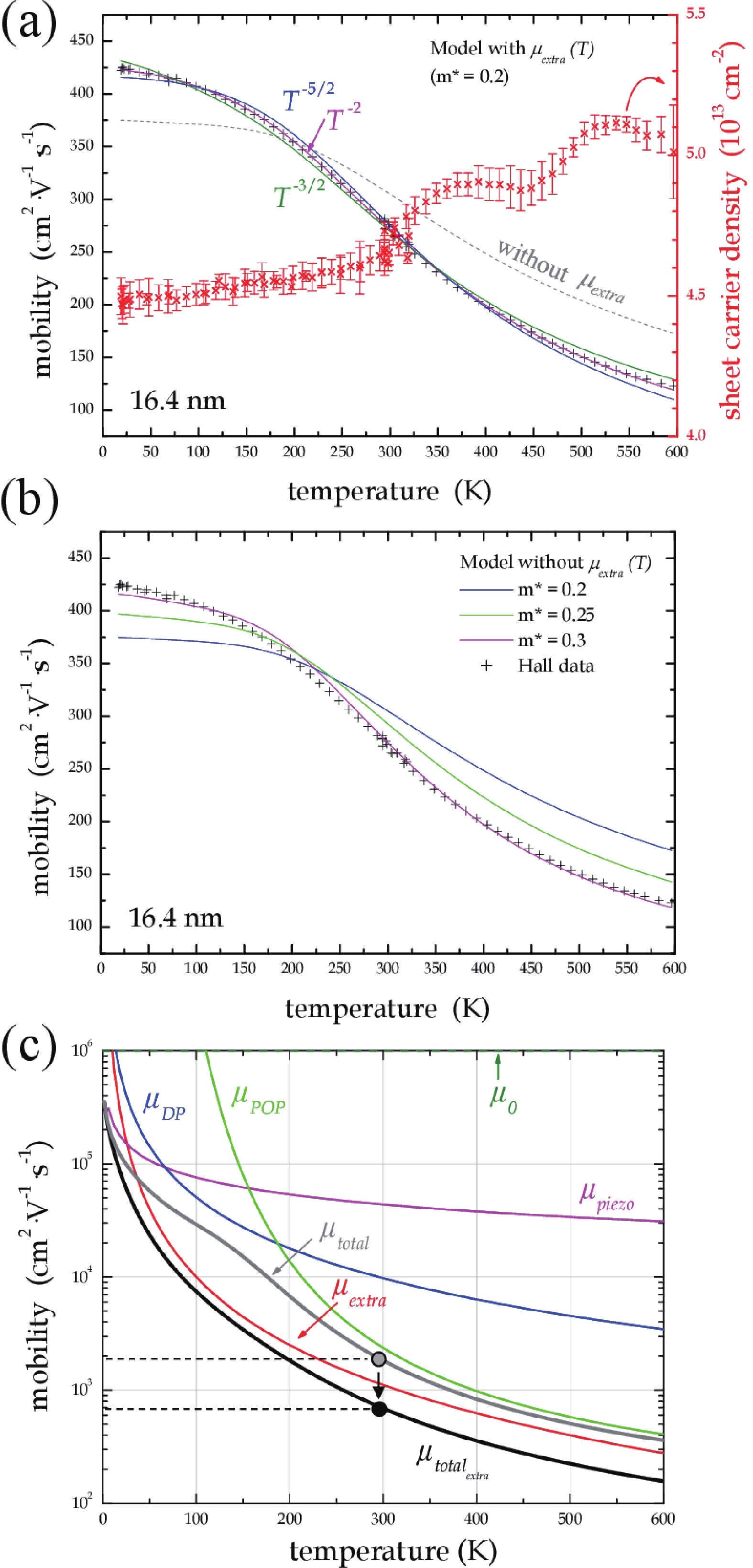
Pristovsek M., Robin Y, Effective mass is limiting the sheet resistance of 2-dimensional electron gases in the III-nitride system. Nature Electronics, submitted
|


 Yoann Robin received his PhD degree in 2014 from the Université de Montpellier. He is a Research Engineer at CNRS (France) and is currently working at IMaSS, Nagoya University, Japan. His research focuses on the growth and characterization of nitride-based compound materials and devices.
 Itsuki Furuhashi is a second year PhD student of electrical engineering at Nagoya University.
 Markus Pristovsek had obtained his PhD in 2000, and during his career stayed at the National Institute of Material Science, Japan, as Assistant Prof. at the Technical University of Berlin, Germany and as Senior Researcher at the University of Cambridge, UK before being appointed in 2017 as Designated Professor in 2017 in the Center for Integrated Research of Future Electronics at the Institute for Materials and Systems for Sustainability of Nagoya University. His interests are the growth of unusual III-V semiconductors and their thorough understanding of the basic physics of such devices.
 DownLoad: