| [1] |
Shatalov M, Sun W H, Lunev A, et al. AlGaN deep-ultraviolet light-emitting diodes with external quantum efficiency above 10%. Appl Phys Express, 2012, 5(8): 082101
|
| [2] |
Takano T, Mino T, Sakai J, et al. Deep-ultraviolet light-emitting diodes with external quantum efficiency higher than 20% at 275 nm achieved by improving light-extraction efficiency. Appl Phys Express, 2017, 10(3): 031002 doi: 10.7567/APEX.10.031002 |
| [3] |
Tsao J Y, Chowdhury S, Hollis M A, et al. Ultrawide-bandgap semiconductors: Research opportunities and challenges. Adv Electron Mater, 2017, 4(1): 1600501
|
| [4] |
Li D B, Jiang K, Sun X J, et al. AlGaN photonics: Recent advances in materials and ultraviolet devices. Adv Opt Photonics, 2018, 10(1): 43 doi: 10.1364/AOP.10.000043 |
| [5] |
Kneissl M, Seong T-Y, Han J, et al. The emergence and prospects of deep-ultraviolet light-emitting diode technologies. Nat Photonics, 2019, 13(4): 233 doi: 10.1038/s41566-019-0359-9 |
| [6] |
Yu R X, Liu G X, Wang G D, et al. Ultrawide-bandgap semiconductor AlN crystals: Growth and applications. J Mater Chem C, 2021, 9(6): 1852 doi: 10.1039/D0TC04182C |
| [7] |
Khan M A, Maeda N, Yun J, et al. Achieving 9.6% efficiency in 304 nm p-AlGaN UVB LED via increasing the holes injection and light reflectance. Sci Rep, 2022, 12(1): 2591 doi: 10.1038/s41598-022-04876-x |
| [8] |
Yuvaraja S, Khandelwal V, Tang X, et al. Wide bandgap semiconductor-based integrated circuits. Chip, 2023, 2(4): 100072 doi: 10.1016/j.chip.2023.100072 |
| [9] |
Khan M A, Yamada Y, Hirayama H. Progress and outlook of 10% efficient AlGaN-based (290–310 nm) band UVB LEDs. Phys Status Solidi A, 2024, 221(13): 2300581
|
| [10] |
Li T, Chen Z Y, Wang T, et al. Residual Al adatoms driven epitaxy of AlGaN QWs for high-performance UV LEDs. Adv Mater, 2025, 37(18): e2501601 doi: 10.1002/adma.202501601 |
| [11] |
Liu S F, Yuan Y, Huang L J, et al. Drive high power UVC-LED wafer into low-cost 4-inch era: effect of strain modulation. Adv Funct Mater, 2022, 32(19): 2112111
|
| [12] |
Susilo N, Ziffer E, Hagedorn S, et al. Improved performance of UVC-LEDs by combination of high-temperature annealing and epitaxially laterally overgrown AlN/sapphire. Photonics Res, 2020, 8(4): 589 doi: 10.1364/PRJ.385275 |
| [13] |
Ban K, Yamamoto J-i, Takeda K, et al. Internal quantum efficiency of whole-composition-range AlGaN multiquantum wells. Appl Phys Express, 2011, 4(5): 052101 doi: 10.1143/APEX.4.052101 |
| [14] |
Tanaka S, Kawase Y, Teramura S, et al. Effect of dislocation density on optical gain and internal loss of AlGaN-based ultraviolet-B band lasers. Appl Phys Express, 2020, 13(4): 045504 doi: 10.35848/1882-0786/ab7caf |
| [15] |
Bai J, Dudley M, Sun W H, et al. Reduction of threading dislocation densities in AlN/sapphire epilayers driven by growth mode modification. Appl Phys Lett, 2006, 88: 051903 doi: 10.1063/1.2170407 |
| [16] |
Hagedorn S, Walde S, Knauer A, et al. Status and prospects of AlN templates on sapphire for ultraviolet light-emitting diodes. Phys Status Solidi A, 2020, 217(14): 1901022 doi: 10.1002/pssa.201901022 |
| [17] |
Fei C L, Liu X L, Zhu B P, et al. AlN piezoelectric thin films for energy harvesting and acoustic devices. Nano Energy, 2018, 51: 146 doi: 10.1016/j.nanoen.2018.06.062 |
| [18] |
Hoque M S B, Koh Y R, Braun J L, et al. High in-plane thermal conductivity of aluminum nitride thin films. ACS Nano, 2021, 15(6): 9588 doi: 10.1021/acsnano.0c09915 |
| [19] |
Liu S F, Yuan Y, Sheng S S, et al. Four-inch high quality crack-free AlN layer grown on a high-temperature annealed AlN template by MOCVD. J Semicond, 2021, 42(12): 122804 doi: 10.1088/1674-4926/42/12/122804 |
| [20] |
Banal R G, Akashi Y, Matsuda K, et al. Crack-free thick AlN films obtained by NH 3 nitridation of sapphire substrates. Jpn J Appl Phys, 2013, 52(8S): 08jb21 doi: 10.7567/JJAP.52.08JB21 |
| [21] |
Yim W M, Paff R J. Thermal expansion of AlN, sapphire, and silicon. J Appl Phys, 1974, 45(3): 1456 doi: 10.1063/1.1663432 |
| [22] |
Miyake H, Nishio G, Suzuki S, et al. Annealing of an AlN buffer layer in N 2–CO for growth of a high-quality AlN film on sapphire. Appl Phys Express, 2016, 9: 025501 doi: 10.7567/APEX.9.025501 |
| [23] |
Ibanez A, Leroux M, Nikitskiy N, et al. The influence of alloy disorder effects on the anisotropy of emission diagrams in (Al, Ga)N quantum wells embedded into AlN barriers. Phys Status Solidi B, 2024, 261(8): 2400215 doi: 10.1002/pssb.202400215 |
| [24] |
Kirihara T, Khan M A, Sharif M N, et al. 225 nm far-UVC LEDs enabled directly on c-sapphire by tailored AlN molar fraction in n-AlGaN layers. J Appl Phys, 2025, 138(17): 174501 doi: 10.1063/5.0276994 |
| [25] |
Bryan I, Bryan Z, Mita S, et al. Surface kinetics in AlN growth: A universal model for the control of surface morphology in III-nitrides. J Cryst Growth, 2016, 438: 81 doi: 10.1016/j.jcrysgro.2015.12.022 |
| [26] |
Jiang K, Sun X J, Ben J W, et al. The defect evolution in homoepitaxial AlN layers grown by high-temperature metal–organic chemical vapor deposition. CrystEngComm, 2018, 20(19): 2720 doi: 10.1039/C8CE00287H |
| [27] |
Jiang K, Ben J W, Sun X J, et al. The AlN lattice-polarity inversion in a high-temperature-annealed c-oriented AlN/sapphire originated from the diffusion of Al and O atoms from sapphire. Nanoscale Adv, 2024, 6(2): 418 doi: 10.1039/D3NA00780D |
| [28] |
Wu H L, He C G, Ge J B, et al. Suppressing dislocations and excess compressive stress in high-temperature-annealed AlN films through macrostep-induced dislocation inclination. Cryst Growth Des, 2025, 25(8): 2347 doi: 10.1021/acs.cgd.4c01272 |
| [29] |
Zhang E T, Ben J W, Nie Z K, et al. Compressive stress management for hillock-free AlGaN epitaxy on HTA-AlN templates using low-Al-content interlayer. J Semicond, 2026, 47(2): 022502 doi: 10.1088/1674-4926/25080020 |
| [30] |
Joo H-Y, Kim H J, Kim S J, et al. Spectrophotometric analysis of aluminum nitride thin films. J Vac Sci Technol A, 1999, 17(3): 862 doi: 10.1116/1.582035 |
| [31] |
Wang T-Y, Tasi C-T, Lin C-F, et al. 85% internal quantum efficiency of 280-nm AlGaN multiple quantum wells by defect engineering. Sci Rep, 2017, 7(1): 14422 doi: 10.1038/s41598-017-14825-8 |
| [32] |
Li T, Luo W, Liu S F, et al. Paving the way for high-performance UVB-LEDs through substrate-dominated strain-modulation. Adv Funct Mater, 2023, 33(3): 2208171
|
| [33] |
Dunn C G, Koch E F. Comparison of dislocation densities of primary and secondary recrystallisation grains of Si–Fe. Acta Metall Mater, 1957, 5: 548
|
| [34] |
Zhang L, Shao Y L, Wu Y Z, et al. Characterization of dislocation etch pits in HVPE-grown GaN using different wet chemical etching methods. J Alloy Compd, 2010, 504(1): 186 doi: 10.1016/j.jallcom.2010.05.085 |
| [35] |
Ponce F A, Cherns D, Young W T, et al. Characterization of dislocations in GaN by transmission electron diffraction and microscopy techniques. Appl Phys Lett, 1996, 69(6): 770 doi: 10.1063/1.117886 |
| [36] |
Khan M A, Maeda N, Jo M, et al. 13 mW operation of a 295–310 nm AlGaN UV-B LED with a p-AlGaN transparent contact layer for real world applications. J Mater Chem C, 2019, 7(1): 143 doi: 10.1039/C8TC03825B |


 Tai Li earned his BE degree from Jilin University in 2019 and his PhD from Peking University in 2024. He is currently a postdoctoral researcher at Peking University. His research interests focus on the MOCVD growth and characterization of III-nitride semiconductors and optoelectronic devices.
 Ziruo Wang got her bachelor’s degree in 2024 from Peking University. Now she is a doctoral student at Peking University under the supervision of Prof. Xinqiang Wang. Her research focuses on the characterization of III-nitride materials using scanning transmission electron microscopy (STEM).
 Ye Yuan got his PhD from Technische Universität Dresden in Germany in 2017. Then he joined Helmholtz-Zentrum Dresden-Rossendorf and King Abdullah University of Science and Technology as postdoc in 2017 and 2018, respectively. In 2019, he joined Songshan Lake Materials Laboratory as an associate investigator. His research mainly focuses on the growth, physics and application of ultra-wide bandgap semiconductors.
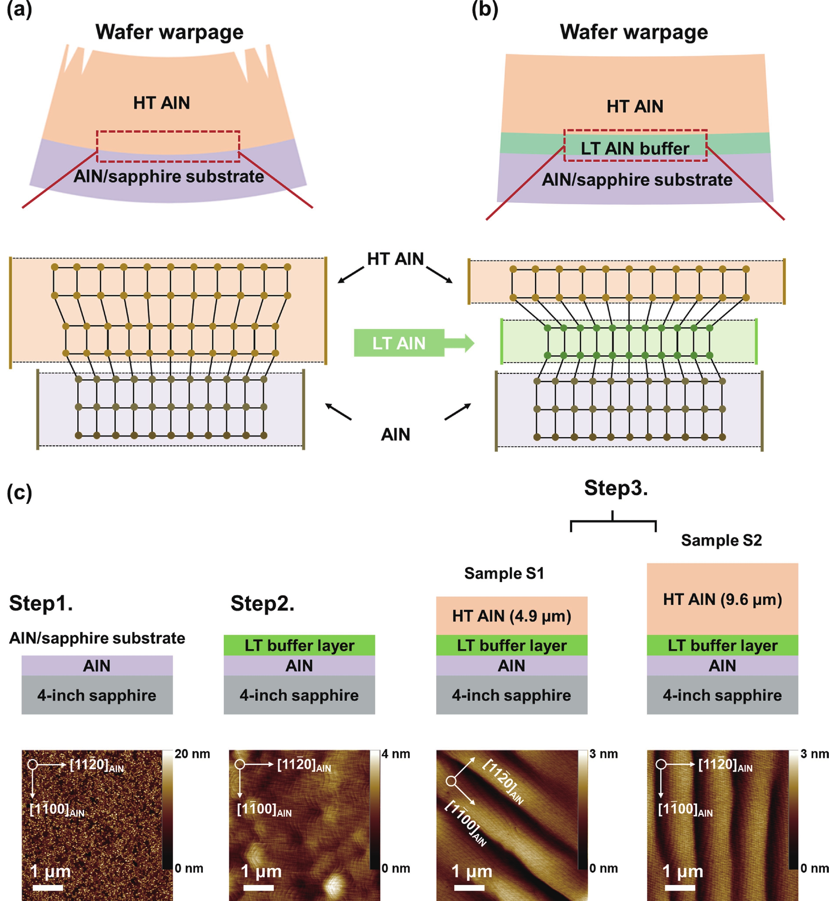
 DownLoad: