| [1] |
Liu Y C, Bai H K, Wang X, et al. Electronic properties and quantum transport behavior of twisted γ-graphdiyne/graphene. Natl Sci Open, 2025, 4(5): 20250036 doi: 10.1360/nso/20250036 |
| [2] |
Dai Y Q, Xiong Y H, Ahmad F, et al. 2D nonlayered materials for transistor application. Adv Phys Res, 2025, 4(6): 2400186 doi: 10.1002/apxr.202400186 |
| [3] |
Mounet N, Gibertini M, Schwaller P, et al. Two-dimensional materials from high-throughput computational exfoliation of experimentally known compounds. Nat Nanotechnol, 2018, 13(3): 246 doi: 10.1038/s41565-017-0035-5 |
| [4] |
Huang X, Li S Z, Huang Y Z, et al. Synthesis of hexagonal close-packed gold nanostructures. Nat Commun, 2011, 2: 292 doi: 10.1038/ncomms1291 |
| [5] |
Zhang X D, Zhang J J, Zhao J Y, et al. Half-metallic ferromagnetism in synthetic Co 9Se 8 nanosheets with atomic thickness. J Am Chem Soc, 2012, 134(29): 11908 doi: 10.1021/ja3046603 |
| [6] |
Cheng W R, He J F, Yao T, et al. Half-unit-cell α-Fe 2O 3 semiconductor nanosheets with intrinsic and robust ferromagnetism. J Am Chem Soc, 2014, 136(29): 10393 doi: 10.1021/ja504088n |
| [7] |
Wang Q S, Wen Y, Yao F R, et al. BN-enabled epitaxy of Pb 1–xSn xSe nanoplates on SiO 2/Si for high-performance mid-infrared detection. Small, 2015, 11(40): 5388 doi: 10.1002/smll.2015020492 |
| [8] |
Huang W J, Gan L, Yang H T, et al. Controlled synthesis of ultrathin 2D β-In 2S 3 with broadband photoresponse by chemical vapor deposition. Adv Funct Mater, 2017, 27(36): 1702448 doi: 10.1002/adfm.201702448 |
| [9] |
Chen Y X, Liu K L, Liu J X, et al. Growth of 2D GaN single crystals on liquid metals. J Am Chem Soc, 2018, 140(48): 16392 doi: 10.1021/jacs.8b08351 |
| [10] |
Gong C H, Chu J W, Yin C J, et al. Self-confined growth of ultrathin 2D nonlayered wide-bandgap semiconductor CuBr flakes. Adv Mater, 2019, 31(36): 1903580 doi: 10.1002/adma.201903580 |
| [11] |
Yin C J, Gong C H, Chu J W, et al. Ultrabroadband photodetectors up to 10.6 µm based on 2D Fe 3O 4 nanosheets. Adv Mater, 2020, 32(25): 2002237 doi: 10.1002/adma.202002237 |
| [12] |
Wang P, Wen Y, Zhao X X, et al. Controllable synthesis quadratic-dependent unsaturated magnetoresistance of two-dimensional nonlayered Fe 7S 8 with robust environmental stability. ACS Nano, 2022, 16(5): 8301 doi: 10.1021/acsnano.2c02267 |
| [13] |
Zhao Z J, Fang Z, Han X C, et al. A general thermodynamics-triggered competitive growth model to guide the synthesis of two-dimensional nonlayered materials. Nat Commun, 2023, 14: 958 doi: 10.1038/s41467-023-36619-5 |
| [14] |
Song L Y, Zhao Y, Xu B Q, et al. Robust multiferroic in interfacial modulation synthesized wafer-scale one-unit-cell of chromium sulfide. Nat Commun, 2024, 15: 721 doi: 10.1038/s41467-024-44929-5 |
| [15] |
Xiong Y H, Xu D, Zou Y S, et al. Vapour–liquid–solid–solid growth of two-dimensional non-layered β-Bi 2O 3 crystals with high hole mobility. Nat Mater, 2025, 24(5): 688 doi: 10.1038/s41563-025-02141-w |
| [16] |
Kim J, Son E, Choi Y, et al. Kinetically tailored chemical vapor deposition approach for synthesizing high-quality large-area non-layered 2D materials. Small, 2025, 21(7): 2410411 doi: 10.1002/smll.202410411 |
| [17] |
Island J O, Steele G A, van der Zant H S J, et al. Thickness dependent interlayer transport in vertical MoS 2 Josephson junctions. 2D Mater, 2016, 3(3): 031002 doi: 10.1088/2053-1583/3/3/031002 |
| [18] |
Wen Y, Wang Q S, Yin L, et al. Epitaxial 2D PbS nanoplates arrays with highly efficient infrared response. Adv Mater, 2016, 28(36): 8051 doi: 10.1002/adma.201602481 |
| [19] |
Lei B C, Li A L, Zhou W Z, et al. Room-temperature ferromagnetism and half-metallicity in monolayer orthorhombic CrS 2. Front Phys, 2024, 19(4): 43200 doi: 10.1007/s11467-023-1387-y |
| [20] |
Li Y, Li F M, Meng X Y, et al. Ultrathin Co 3O 4 nanomeshes for the oxygen evolution reaction. ACS Catal, 2018, 8(3): 1913 doi: 10.1021/acscatal.7b03949 |


 Yongqi Dai received his bachelor’s degree from Nanjing Tech University in 2022. He is currently a Ph.D. candidate under the supervision of Prof. Xiang Chen in the School of Materials Science and Engineering at Nanjing University of Science and Technology. His research is focused on the controllable synthesis and transistor application of 2D non-layered metal oxide semiconductors.
 Xin Wang received his bachelor’s degree in 2023 from Shenyang Jianzhu University. He is currently pursuing his Ph.D. in the School of Materials Science and Engineering at Nanjing University of Science and Technology, under the supervision of Prof. Xiang Chen and Prof. Haibo Zeng. His research primarily focuses on the CVD-controlled synthesis of two-dimensional oxide semiconductors and their applications in electronics.
 Xiang Chen is currently a full professor at the School of Materials Science and Engineering, Nanjing University of Science and Technology (NJUST). He received his Ph.D. from the University of Science and Technology Beijing in 2014 and worked as a research professor at Yonsei University from 2014 to 2018. His main research interest is the controllable and wafer-scale synthesis of p-type 2D semiconductors and their applications in high-performance, low-power integrated electronics.
 Haibo Zeng received his Ph.D. degree from the Institute of Solid State Physics, Chinese Academy of Sciences in 2006. He later worked with Prof. Claus Klingshirn in 2007 at the University of Karlsruhe, Germany. In 2008, he joined Prof. Yoshio Bando’s group at the National Institute for Materials Science (NIMS), Japan. In 2011, he returned to Nanjing University of Aeronautics and Astronautics as a full professor, and then moved to Nanjing University of Science and Technology in 2013 as a distinguished professor and Director of the Institute of Optoelectronics & Nanomaterials. His current research interest is functional perovskite materials and devices.
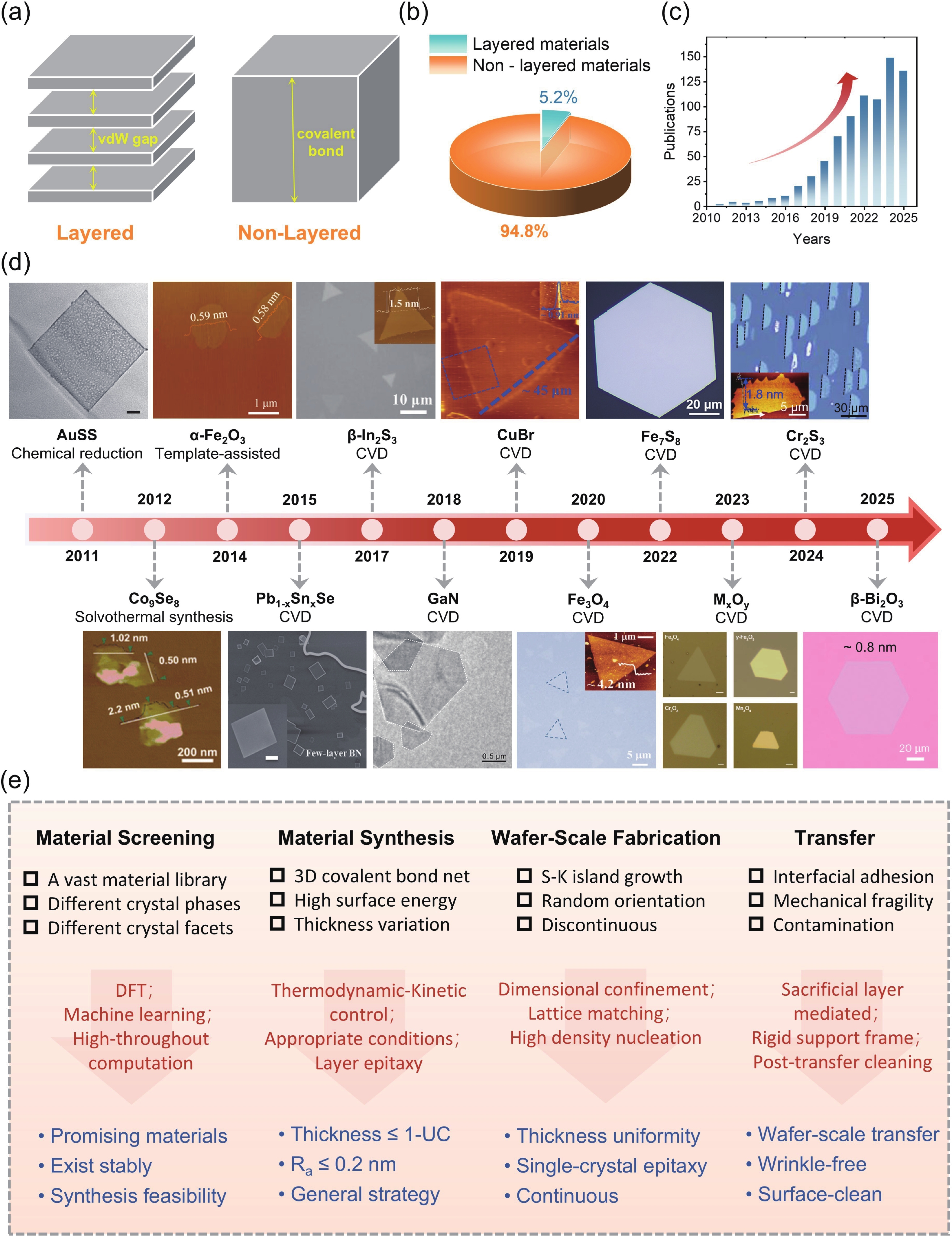
 DownLoad: