| [1] |
Tang J C, Li S X, Zhan L, et al. Contact engineering for two-dimensional van der Waals semiconductors. Mater Today Electron, 2025, 11: 100132 doi: 10.1016/j.mtelec.2024.100132 |
| [2] |
Ma L K, Wang Y L, Liu Y. Van der Waals contact for two-dimensional transition metal dichalcogenides. Chem Rev, 2024, 124(5): 2583 doi: 10.1021/acs.chemrev.3c00697 |
| [3] |
Liu Y, Guo J, Zhu E B, et al. Approaching the Schottky-Mott limit in van der Waals metal-semiconductor junctions. Nature, 2018, 557(7707): 696
|
| [4] |
Kwon G, Choi Y H, Lee H, et al. Interaction- and defect-free van der Waals contacts between metals and two-dimensional semiconductors. Nat Electron, 2022, 5(4): 241 doi: 10.1038/s41928-022-00746-6 |
| [5] |
Wang Y, Kim J C, Wu R J, et al. Van der Waals contacts between three-dimensional metals and two-dimensional semiconductors. Nature, 2019, 568(7750): 70 doi: 10.1038/s41586-019-1052-3 |
| [6] |
Avsar A, Ochoa H, Guinea F, et al. Colloquium: Spintronics in graphene and other two-dimensional materials. Rev Mod Phys, 2020, 92(2): 021003 doi: 10.1103/RevModPhys.92.021003 |
| [7] |
Schmidt G, Ferrand D, Molenkamp L W, et al. Fundamental obstacle for electrical spin injection from a ferromagnetic metal into a diffusive semiconductor. Phys Rev B, 2000, 62(8): R4790 doi: 10.1103/PhysRevB.62.R4790 |
| [8] |
Han W, Pi K, Bao W, et al. Electrical detection of spin precession in single layer graphene spin valves with transparent contacts. Appl Phys Lett, 2009, 94(22): 222109 doi: 10.1063/1.3147203 |
| [9] |
Rashba E I. Theory of electrical spin injection: Tunnel contacts as a solution of the conductivity mismatch problem. Phys Rev B, 2000, 62(24): R16267 doi: 10.1103/PhysRevB.62.R16267 |
| [10] |
Tombros N, Jozsa C, Popinciuc M, et al. Electronic spin transport and spin precession in single graphene layers at room temperature. Nature, 2007, 448(7153): 571 doi: 10.1038/nature06037 |
| [11] |
Zhou J, Lu X Y, Yang J J, et al. Intrinsic spin transport properties observed in contamination-free graphene-based spin valve. Carbon, 2024, 228: 119321 doi: 10.1016/j.carbon.2024.119321 |
| [12] |
Han W, Pi K, McCreary K M, et al. Tunneling spin injection into single layer graphene. Phys Rev Lett, 2010, 105(16): 167202 doi: 10.1103/PhysRevLett.105.167202 |
| [13] |
Singh S, Katoch J, Xu J S, et al. Nanosecond spin relaxation times in single layer graphene spin valves with hexagonal boron nitride tunnel barriers. Appl Phys Lett, 2016, 109(12): 122411 doi: 10.1063/1.4962635 |
| [14] |
Gurram M, Omar S, Zihlmann S, et al. Spin transport in two-layer-CVD-hBN/graphene/hBN heterostructures. Phys Rev B, 2018, 97(4): 045411 doi: 10.1103/PhysRevB.97.045411 |
| [15] |
Kamalakar M V, Dankert A, Kelly P J, et al. Inversion of spin signal and spin filtering in Ferromagnet| Hexagonal boron nitride-graphene van der Waals heterostructures. Sci Rep, 2016, 6: 21168 doi: 10.1038/srep21168 |
| [16] |
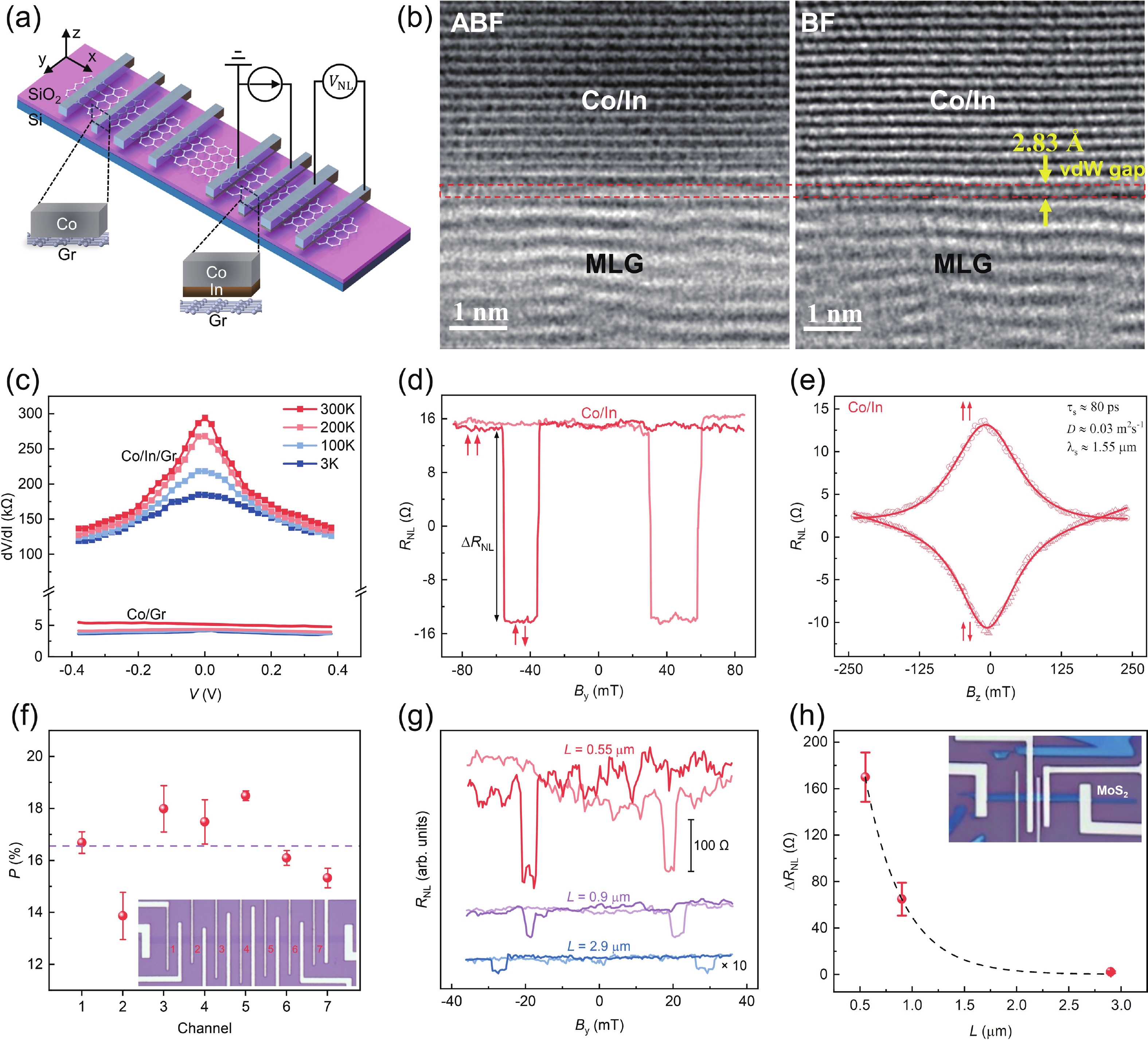
Sarkar S, Oh S, Newton P J, et al. Spin injection in graphene using ferromagnetic van der Waals contacts of indium and cobalt. Nat Electron, 2025, 8(3): 215 doi: 10.1038/s41928-024-01330-w |
| [17] |
Huang S M, Hou F C, Qu T Y, et al. Room-temperature high-efficiency spin injection via van der Waals tunnel contact. Nat Commun, 2026, 17: 1228 doi: 10.1038/s41467-025-67989-7 |
| [18] |
Tho C C, Yang Z M, Fang S B, et al. Computational design of two-dimensional MA2Z4 family field-effect transistor for future Ångström-scale CMOS technology nodes. InfoMat, 2026, 8(2): e70096
|
| [19] |
Bai L, Feng W X, Liu S Y, et al. Altermagnetism: Exploring new frontiers in magnetism and spintronics. Adv Funct Mater, 2024, 34(49): 2409327 doi: 10.1002/adfm.202409327 |


 Rong Zhang Zhang Rong, Academician of the Chinese Academy of Sciences, is a professor at Xiamen University. He obtained his B. S. and Ph. D. from Nanjing University in 1983 and 1995 respectively. He has long been dedicated to research on new semiconductor materials, devices, and physics, and is one of China's pioneer scientists engaged in the study of wide-bandgap semiconductors.
 Deyi Fu is an associate professor at College of Physical Science and Engineering, Xiamen University. He obtained his Ph.D. in microelectronics and solid-state electronics from Nanjing University in 2012. His doctoral dissertation was honored as the Outstanding Doctoral Dissertation of Jiangsu Province in 2013. From 2012 to 2020, he conducted postdoctoral research successively at University of California, Berkeley and National University of Singapore. His current research focuses on two-dimensional spintronic materials, physics and devices.
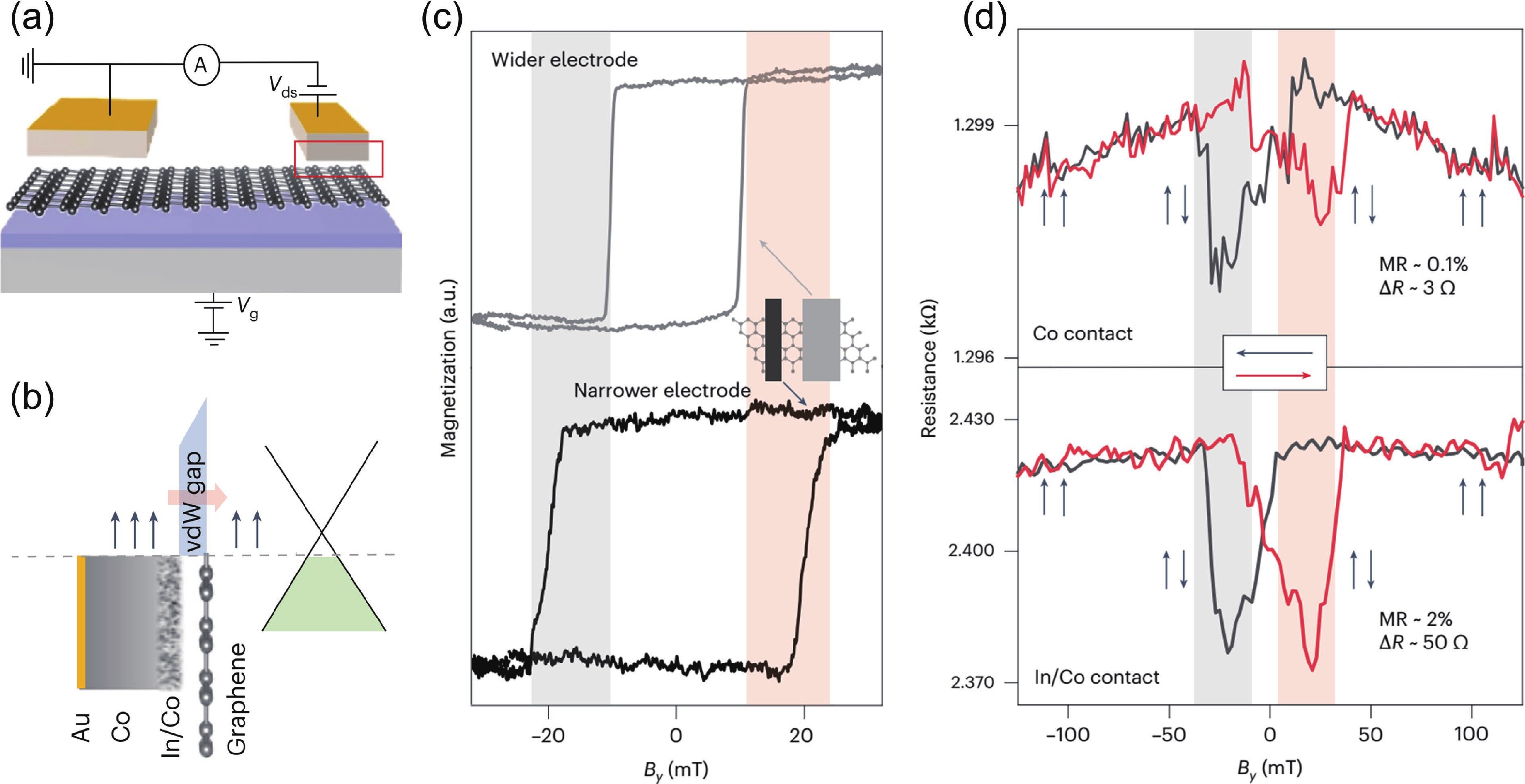
 DownLoad: