| [1] |
Liu Q C, Wei T, Zheng Y H, et al. Picosecond operation of optoelectronic hybrid phase change memory based on Si-doped Sb films. Adv Funct Mater, 2025, 35(11): 2417128 doi: 10.1002/adfm.202417128 |
| [2] |
Wu B, Wei T, Hu J, et al. Thermal stability and high speed for optoelectronic hybrid phase-change memory based on Cr doped Ge 2Sb 2Te 5 thin film. Ceram Int, 2023, 49(23): 37837 doi: 10.1016/j.ceramint.2023.09.112 |
| [3] |
Wei T, Wang Q, Song S N, et al. Reversible phase-change characteristics and structural origin in Cr doped Ge 2Sb 2Te 5 thin films. Thin Solid Films, 2020, 716: 138434 doi: 10.1016/j.tsf.2020.138434 |
| [4] |
Wang H, Lu Z L, Qi Z, et al. Preparation and oxidation resistance study of silicon nitride coatings on graphite surfaces by chemical vapor deposition. Carbon Technol., 2023, 42(01): 34
|
| [5] |
Shangguan D D, Wang B L, Wang C, et al. Fabrication and properties of a dense SiC NWs-toughened α-Si 3N 4 composite coating on porous Si 3N 4 ceramics. Int J Appl Ceram Technol, 2020, 17(2): 501 doi: 10.1111/ijac.13419 |
| [6] |
Kamataki K, Sasaki Y, Nagao I, et al. Low-temperature fabrication of silicon nitride thin films from a SiH 4+N2 gas mixture by controlling SiN x nanoparticle growth in multi-hollow remote plasma chemical vapor deposition. Mater Sci Semicond Process, 2023, 164: 107613 doi: 10.1016/j.mssp.2023.107613 |
| [7] |
Minh N Q, Van Nong N, Oda O, et al. Low-temperature growth at 225 °C and characterization of carbon nanowalls synthesized by radical injection plasma-enhanced chemical vapor deposition. Vacuum, 2024, 224: 113180 doi: 10.1016/j.vacuum.2024.113180 |
| [8] |
Surana V K, Ganguly S, Saha D. Performance improvement in AlGaN/GaN high-electron-mobility transistors by low-temperature inductively coupled plasma–chemical vapor deposited SiN x as gate dielectric and surface passivation. Phys Status Solidi A, 2022, 219(24): 2200509 doi: 10.1002/pssa.202200509 |
| [9] |
Zhang C, Wu M, Wang P C, et al. Stability of SiN x prepared by plasma-enhanced chemical vapor deposition at low temperature. Nanomaterials, 2021, 11(12): 3363 doi: 10.3390/nano11123363 |
| [10] |
Rogov A B, Shayapov V R. The role of cathodic current in PEO of aluminum: Influence of cationic electrolyte composition on the transient current-voltage curves and the discharges optical emission spectra. Appl Surf Sci, 2017, 394: 323 doi: 10.1016/j.apsusc.2016.10.115 |
| [11] |
Kasalica B, Radić-Perić J, Perić M, et al. The mechanism of evolution of microdischarges at the beginning of the PEO process on aluminum. Surf Coat Technol, 2016, 298: 24 doi: 10.1016/j.surfcoat.2016.04.044 |
| [12] |
Troughton S C, Nominé A, Dean J, et al. Effect of individual discharge cascades on the microstructure of plasma electrolytic oxidation coatings. Appl Surf Sci, 2016, 389: 260 doi: 10.1016/j.apsusc.2016.07.106 |
| [13] |
Oleksak R P, Devaraj A, Herman G S. Atomic-scale structural evolution of Ta–Ni–Si amorphous metal thin films. Mater Lett, 2016, 164: 9 doi: 10.1016/j.matlet.2015.10.112 |
| [14] |
Naghdali S, Schiester M, Waldl H, et al. Improving the elemental and imaging accuracy in atom probe tomography of (Ti, Si)N single and multilayer coatings using isotopic substitution of N. Ultramicroscopy, 2025, 276: 114200 doi: 10.1016/j.ultramic.2025.114200 |
| [15] |
Nekipelov S V, Sekushin N A, Krzhizhanovskaya M G, et al. Electrical and optical properties and XPS spectra of pyrochlore Bi 1.65Mn 0.5Cr 0.5Nb 2O 9 -. Ceram Int, 2025, 51(19): 28587 doi: 10.1016/j.ceramint.2025.04.068 |
| [16] |
Olaniyan I, Blázquez Martínez A, Hevelke V V, et al. Optically induced irreversible ferroelastic and ferroelectric switching in epitaxial BaTiO 3 films on silicon. ACS Nano, 2025, 19(43): 37534 doi: 10.1021/acsnano.5c05309 |
| [17] |
Park Y, Shin Y E, Park J, et al. Ferroelectric multilayer nanocomposites with polarization and stress concentration structures for enhanced triboelectric performances. ACS Nano, 2020, 14(6): 7101 doi: 10.1021/acsnano.0c01865 |
| [18] |
Wen J L, Ma T B, Zhang W W, et al. Atomistic insights into Cu chemical mechanical polishing mechanism in aqueous hydrogen peroxide and glycine: ReaxFF reactive molecular dynamics simulations. J Phys Chem C, 2019, 123(43): 26467 doi: 10.1021/acs.jpcc.9b08466 |
| [19] |
Gao F, Weber W J. Atomic-scale simulations of cascade overlap and damage evolution in silicon carbide. J Mater Res, 2003, 18(8): 1877 doi: 10.1557/JMR.2003.0262 |
| [20] |
Elmas S, Rafighi M, Mohammadigharehbagh R, et al. Preparation of semi-transparent V 2AlC thin films using the thermionic vacuum arc technique: Crystal and substrate effects on the electrochemical performance. Eur Phys J Plus, 2026, 141(3): 339 doi: 10.1140/epjp/s13360-026-07506-x |
| [21] |
Chen J W, Zhao Y K, Guo Y J, et al. Unveiling the substrate effect: A combined experimental and simulation study of field emission from carbon nanotubes on stainless steel and silicon. Electron Mater Lett, 2026: 1
|
| [22] |
Kang X X, Zhong X L, Chen Z F, et al. Development and characterization of high temperature plasma nitridation process for advanced CMOS technology application. 2021 IEEE 14th International Conference on ASIC (ASICON), 2021: 1
|
| [23] |
Shi S J, Cui H P, Tian H C, et al. Exploring a new method for high-performance TPSiV preparation through innovative Si–H/Pt curing system in VSR/TPU blends. E Polym, 2024, 24: 20240081 doi: 10.1515/epoly-2024-0081 |
| [24] |
Sinha A K, Levinstein H J, Smith T E, et al. Reactive plasma deposited Si-N films for MOS-LSI passivation. J Electrochem Soc, 1978, 125(4): 601 doi: 10.1149/1.2131509 |
| [25] |
Miklaszewska P, Aszyk M, Sowiński P, et al. Chromogenic azomacrocycles with imidazole residue–Part II: Effect of spacer type and N–H orientation on chromogenic and spectroscopic properties. Dyes Pigm, 2026, 251: 113696 doi: 10.1016/j.dyepig.2026.113696 |
| [26] |
Li L, Song S N, Zhang Z H, et al. Superlattice-like film for high data retention and high speed phase change random access memory. Solid State Electron, 2016, 120: 52 doi: 10.1016/j.sse.2016.03.005 |
| [27] |
Miao L, Chen L. Interfacial reliability of Al/Sb 2Te 3 and W/Sb 2Te 3 for phase change memory application. Mater Sci Semicond Process, 2025, 199: 109876 doi: 10.1016/j.mssp.2025.109876 |



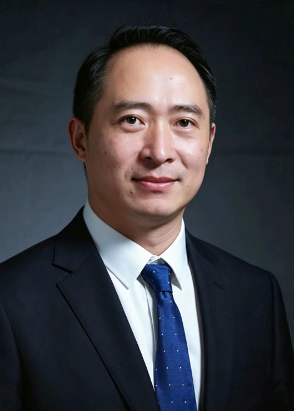 Wanchun Ren received his Ph.D. from University of Chinese Academy of Sciences in 2013. He is currently a teacher at Southwest University of Science and Technology. His research interests include MEMS device and reliability.
 Chun Li is currently a master student at Southwest University of Science and Technology, under the supervision of Dr. Wanchun Ren. Her research focuses on magnetoelectric heterostructures.
 Dan Chen is a master student at Southwest University of Science and Technology, under the supervision of Dr. Wanchun Ren. Her main research direction is microelectronic packaging.
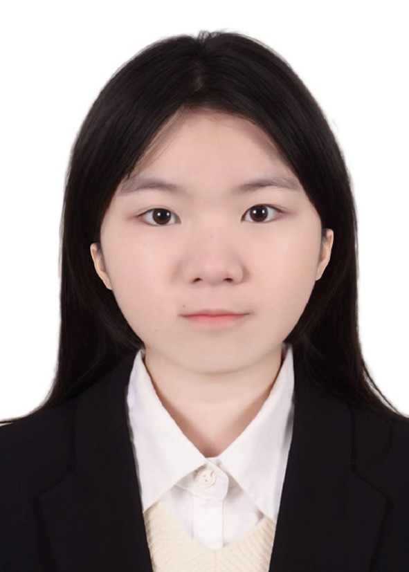 Qian Gao is a master student at Southwest University of Science and Technology under the supervision of Dr. Wanchun Ren. Her research focuses on thin-film bulk acoustic wave materials and devices.
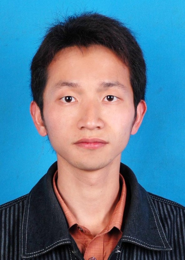 Peng Bi received his Ph.D. from Sichuan University in 2013. He is currently a teacher at Southwest University of Science and Technology. His research interests include computational physics and computational materials science.
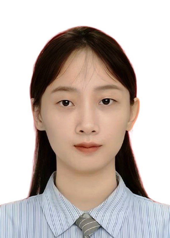 Jingdan Deng is a master student at Southwest University of Science and Technology under the supervision of Dr. Wanchun Ren. Her research focuses on readout circuit for bulk acoustic wave magnetic field sensors.
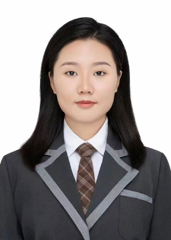 Tianyu Ma is an undergraduate student at Southwest University of Science and Technology, under the supervision of Dr. Wanchun Ren. Her research interests primarily focus on lithography and battery management systems.
 Tingting Liu received her Ph.D. from USTC in 2015. She is currently an associate professor at Southwest University of Science and Technology. Her research interests include microfluidics and MEMS devices.
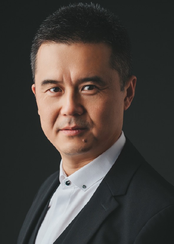 Yang Gao received his Ph.D. from Beijing Institute of Technology in 2000. He is a professor at Southwest University of Science and Technology. His research interests include advanced MEMS devices and their applications.
 Huihui Guo received his Ph.D. from Southwest Jiaotong University in 2013. He is a professor at Southwest University of Science and Technology. His research primarily focuses on gas sensor technology and MEMS/NEMS devices.
 DownLoad: