


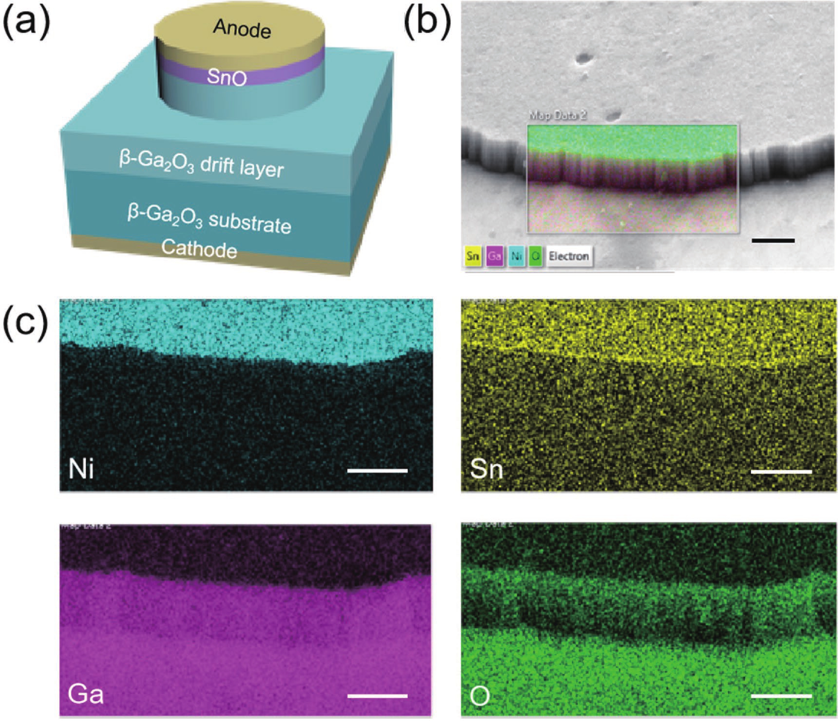
Fig. 1.
(Color online) (a) Schematic of SnO/β-Ga2O3 mesa-HJD. (b) Bird-view SEM image of a typical device and (c) EDS elemental mapping corresponding to the region marked by the square in (b). Scale bar: 2 μm.
ARTICLES
Xinwang Yao, Lizhi Cui, Junwei Zhang, Junhan Qian, Xiaoping Yang, Xiujuan Wang, Chunyan Wu and Linbao Luo
Corresponding author: Chunyan Wu, cywu@hfut.edu.cn
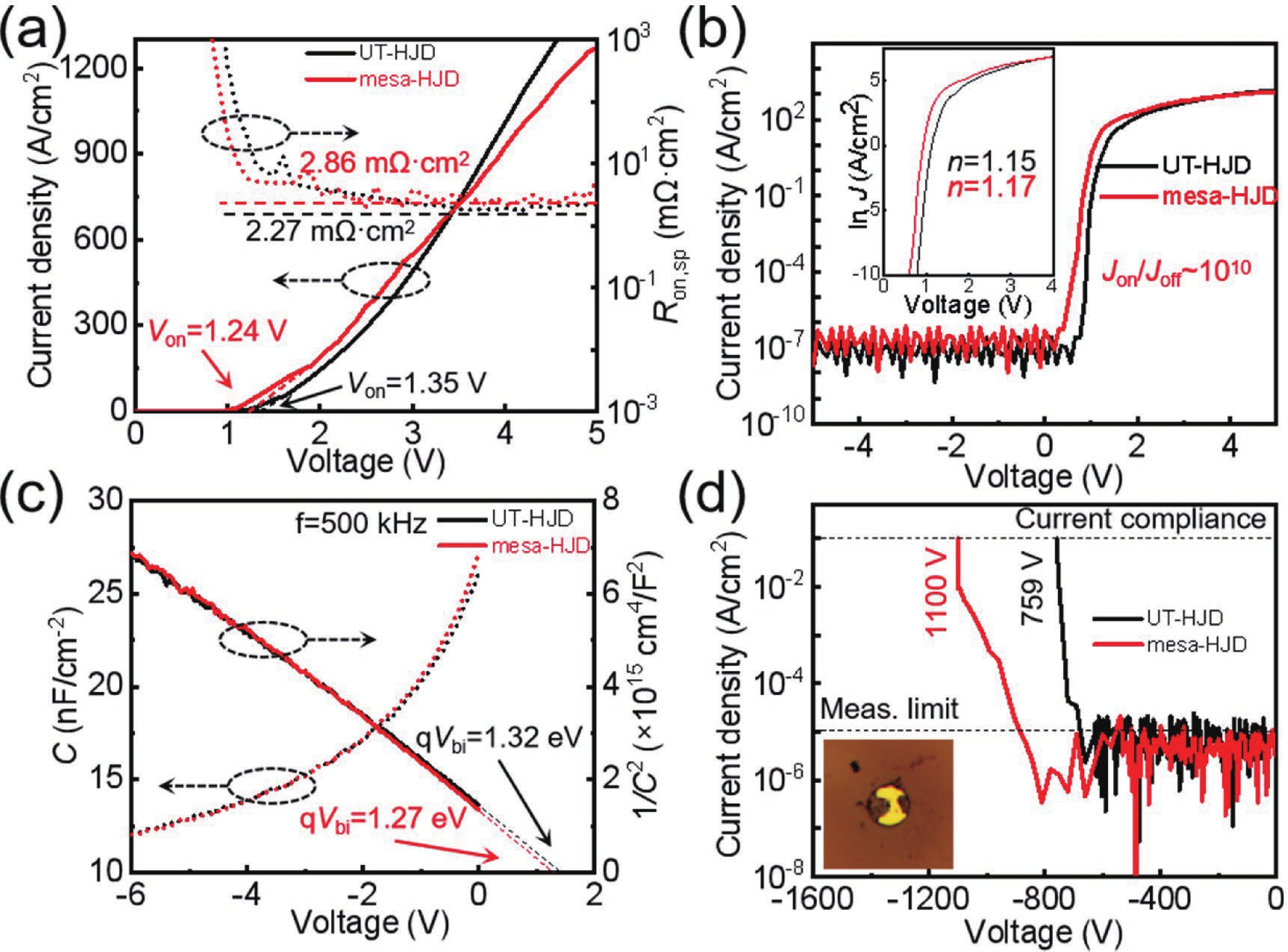
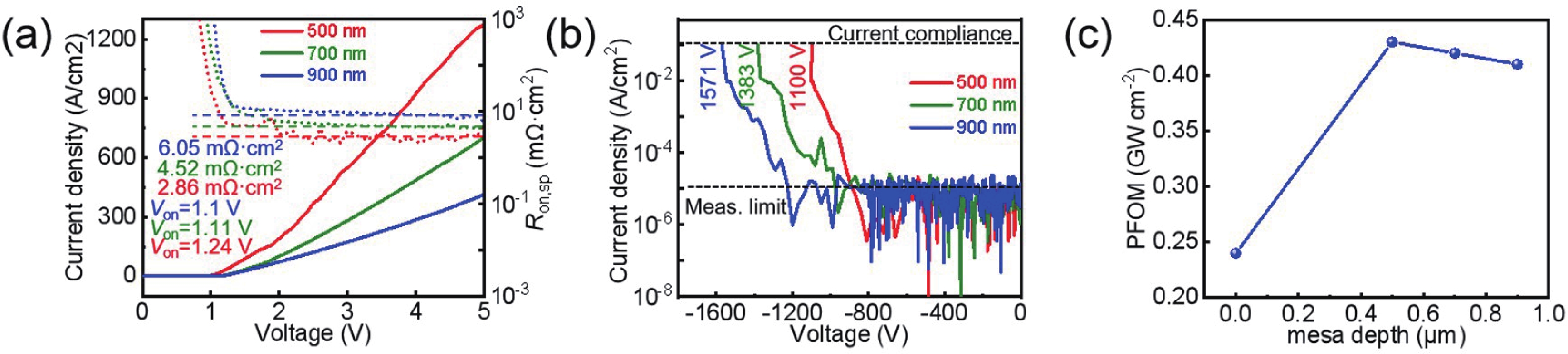
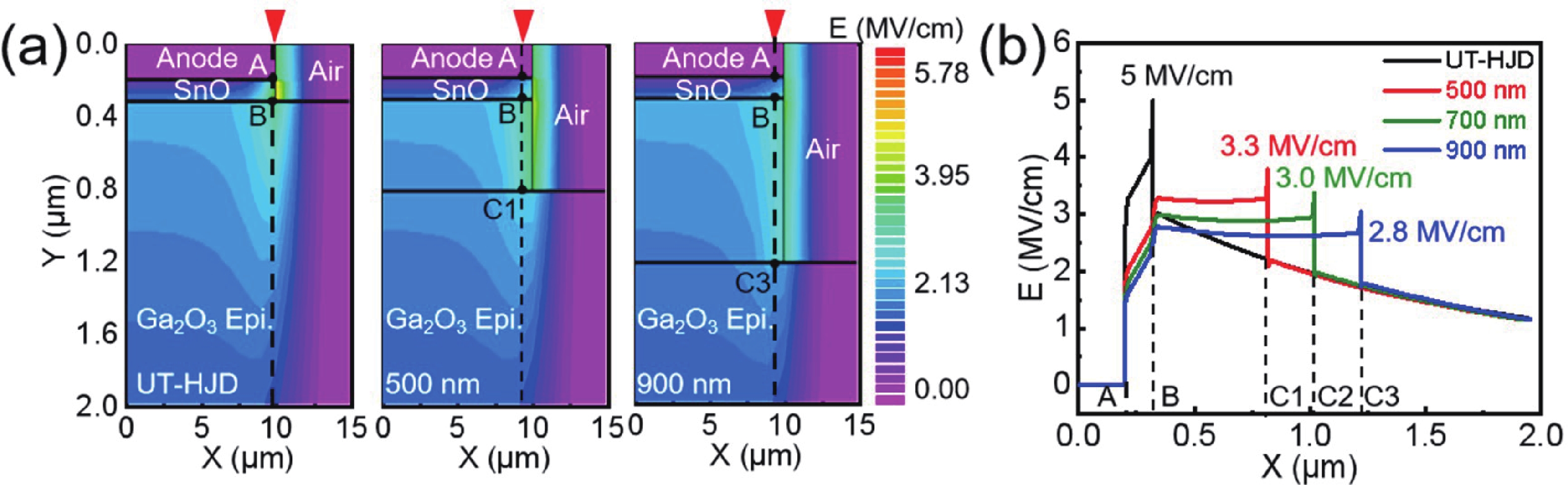
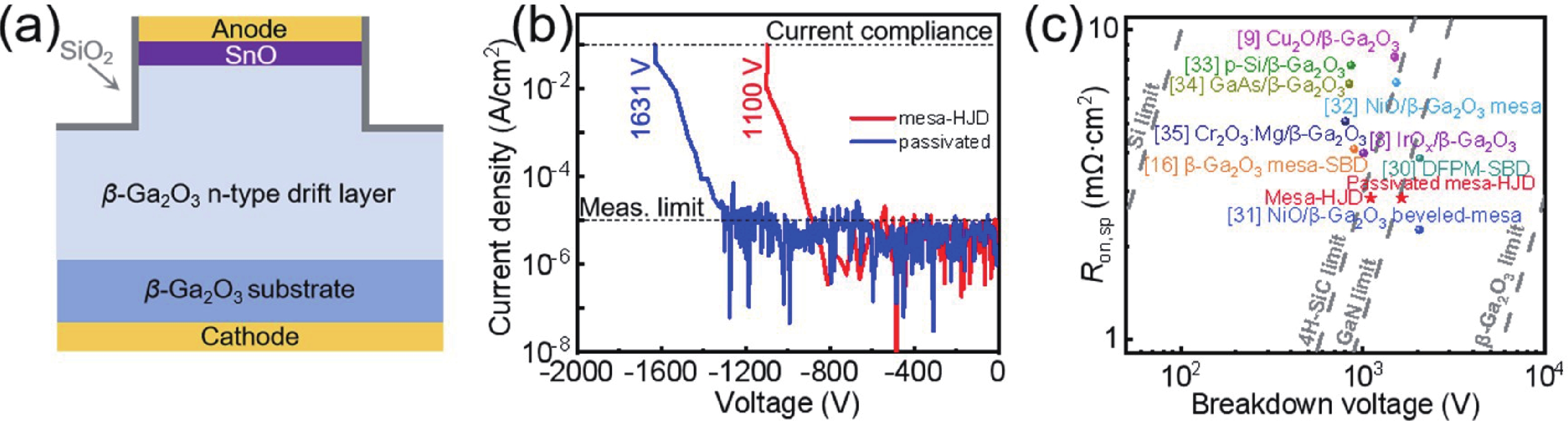
Abstract: In this article, a vertical SnO/β-Ga2O3 mesa heterojunction diode (mesa-HJD) fabricated through self-aligned etching is reported. The mesa structure eliminates the influence of lateral depletion at the region, leading to an improved breakdown characteristics in comparison with its unterminated heterojunction diode (UT-HJD) counterpart. The SnO/β-Ga2O3 mesa-HJD, featuring a 500 nm mesa depth, achieves a breakdown voltage (BV) of 1100 V, which can be improved to 1631 V by sidewall passivation. With the increase of mesa depth, BV increases, accompanied by the increase of specific on-resistance (Ron,sp). Therefore, a maximum Baliga’s power figure of merit (PFOM) can be achieved for the optimized device with 500 nm mesa depth, giving the value of 0.93 GW/cm2 for the passivated device. The mesa-HJD demonstrates considerable potential for application in high BV β-Ga2O3 power electronic devices in the future.
Key words: β-Ga2O3, mesa heterojunction diode (mesa-HJD), power electronic device
| [1] |
Sun S H, Wang C L, Alghamdi S, et al. Recent advanced ultra-wide bandgap β-Ga2O3 material and device technologies. Adv Electron Mater, 2025, 11(1): 2300844 doi: 10.1002/aelm.202300844
|
| [2] |
Wong M H, Higashiwaki M. Vertical β-Ga2O3 power transistors: A review. IEEE Trans Electron Devices, 2020, 67(10): 3925 doi: 10.1109/TED.2020.3016609
|
| [3] |
Yang J C, Ahn S, Ren F, et al. High reverse breakdown voltage Schottky rectifiers without edge termination on Ga2O3. Appl Phys Lett, 2017, 110(19): 192101 doi: 10.1063/1.4983203
|
| [4] |
Li W S, Saraswat D, Long Y Y, et al. Near-ideal reverse leakage current and practical maximum electric field in β-Ga2O3 Schottky barrier diodes. Appl Phys Lett, 2020, 116(19): 192101 doi: 10.1063/5.0007715
|
| [5] |
Han Z, Jian G Z, Zhou X Z, et al. 2.7 kV low leakage vertical PtOx/β-Ga2O3 Schottky barrier diodes with self-aligned mesa termination. IEEE Electron Device Lett, 2023, 44(10): 1680 doi: 10.1109/LED.2023.3305389
|
| [6] |
Lu X, Zhou X D, Jiang H X, et al. 1-kV sputtered p-NiO/n-Ga2O3 heterojunction diodes with an ultra-low leakage current below 1 μA/cm2. IEEE Electron Device Lett, 2020, 41(3): 449 doi: 10.1109/LED.2020.2967418
|
| [7] |
Kokubun Y, Kubo S, Nakagomi S. All-oxide p–n heterojunction diodes comprising p-type NiO and n-type β-Ga2O3. Appl Phys Express, 2016, 9(9): 091101 doi: 10.7567/APEX.9.091101
|
| [8] |
Zheng R T, Feng W Y, Liao C, et al. P-IrOx/n-β-Ga2O3 heterojunction diodes with 1-kV breakdown and ultralow leakage current below 0.1 μA/cm2. IEEE Trans Electron Devices, 2024, 71(3): 1587
|
| [9] |
Watahiki T, Yuda Y, Furukawa A, et al. Heterojunction p-Cu2O/n-Ga2O3 diode with high breakdown voltage. Appl Phys Lett, 2017, 111(22): 222104 doi: 10.1063/1.4998311
|
| [10] |
Wu X, Huang C Y, Xu X X, et al. Band alignment of SnO/β-Ga2O3 heterojunction and its electrical properties for power device application. J Semicond, 2025, 46(8): 082503 doi: 10.1088/1674-4926/25020008
|
| [11] |
Than P H, Than T Q, Takaki Y. Breakdown voltage enhancement in p-GaAs/n-Ga2O3 heterojunction diodes with advanced termination designs. Phys Scr, 2025, 100(7): 075022 doi: 10.1088/1402-4896/addf8f
|
| [12] |
Roy S, Bhattacharyya A, Peterson C, et al. 2.1 kV (001)-β-Ga2O3 vertical Schottky barrier diode with high-k oxide field plate. Appl Phys Lett, 2023, 122(15): 152101 doi: 10.1063/5.0137935
|
| [13] |
Lin C H, Yuda Y, Wong M H, et al. Vertical Ga2O3 Schottky barrier diodes with guard ring formed by nitrogen-ion implantation. IEEE Electron Device Lett, 2019, 40(9): 1487 doi: 10.1109/LED.2019.2927790
|
| [14] |
Wang B Y, Xiao M, Spencer J, et al. 2.5 kV vertical Ga2O3 Schottky rectifier with graded junction termination extension. IEEE Electron Device Lett, 2023, 44(2): 221 doi: 10.1109/LED.2022.3229222
|
| [15] |
Lu X, Zhang X, Jiang H X, et al. Vertical β-Ga2O3 Schottky barrier diodes with enhanced breakdown voltage and high switching performance. Phys Status Solidi A, 2020, 217(3): 1900497 doi: 10.1002/pssa.201900497
|
| [16] |
Wu F H, Han Z, Liu J Y, et al. 8.7 A/700 V β-Ga2O3 Schottky barrier diode demonstrated by oxygen annealing combined with self-aligned mesa termination. Appl Phys Express, 2024, 17(3): 036504 doi: 10.35848/1882-0786/ad2d73
|
| [17] |
Xu X R, Deng Y C, Li T T, et al. Over 2 GW/cm2 low-conduction loss Ga2O3 vertical SBD with self-aligned field plate and mesa termination. Appl Phys Lett, 2024, 125(2): 022106 doi: 10.1063/5.0212785
|
| [18] |
Alfieri G, Mihaila A, Godignon P, et al. Deep level study of chlorine-based dry etched β-Ga2O3. J Appl Phys, 2021, 130(2): 025701 doi: 10.1063/5.0050416
|
| [19] |
Zhang Y H, Mei Z X, Wang T, et al. Flexible transparent high-voltage diodes for energy management in wearable electronics. Nano Energy, 2017, 40: 289 doi: 10.1016/j.nanoen.2017.08.025
|
| [20] |
Martínez-Angeles W L, González-Reynoso O, Carbajal-Arizaga G G, et al. Electronic barriers behavioral analysis of a Schottky diode structure featuring two-dimensional MoS2. Electronics, 2024, 13(20): 4008 doi: 10.3390/electronics13204008
|
| [21] |
Feng Y T, Zhou H, Ma J Y, et al. 120 A/1.78 kV p-Cr2O3/n-β-Ga2O3 heterojunction PN diodes with slanted mesa edge termination. IEEE Electron Device Lett, 2025, 46(10): 1705 doi: 10.1109/LED.2025.3598936
|
| [22] |
Zhao X X, Zhang S M, Shao G Q, et al. Over 450 V breakdown voltage in diamond vertical Schottky barrier diodes with anodic self-aligned mesa termination. Appl Phys Lett, 2025, 127(3): 032107 doi: 10.1063/5.0274905
|
| [23] |
Yang J C, Ren F, Khanna R, et al. Annealing of dry etch damage in metallized and bare (-201) Ga2O3. J Vac Sci Technol B, 2017, 35(5): 051201 doi: 10.1116/1.4986300
|
| [24] |
Sun Y, Kang X W, Zheng Y K, et al. Review of the recent progress on GaN-based vertical power Schottky barrier diodes (SBDs). Electronics, 2019, 8(5): 575 doi: 10.3390/electronics8050575
|
| [25] |
Dhara S, Kalarickal N K, Dheenan A, et al. β-Ga2O3 Schottky barrier diodes with 4.1 MV/cm field strength by deep plasma etching field-termination. Appl Phys Lett, 2022, 121(20): 203501 doi: 10.1063/5.0123284
|
| [26] |
Eifert B, Becker M, Reindl C T, et al. Raman studies of the intermediate tin-oxide phase. Phys Rev Mater, 2017, 1: 014602 doi: 10.1103/PhysRevMaterials.1.014602
|
| [27] |
Hudgins J L, Simin G S, Santi E, et al. An assessment of wide bandgap semiconductors for power devices. IEEE Trans Power Electron, 2003, 18(3): 907 doi: 10.1109/TPEL.2003.810840
|
| [28] |
Zhang L H, Verma A, Xing H G, et al. Inductively-coupled-plasma reactive ion etching of single-crystal β-Ga2O3. Jpn J Appl Phys, 2017, 56(3): 030304 doi: 10.7567/JJAP.56.030304
|
| [29] |
Wei S B, Hong Z F, Li C C, et al. Increase fixed charge at Al2O3/Ga2O3 interface for high-performance Ga2O3 trench Schottky barrier diodes by atomic nitrogen treatment. Appl Phys Lett, 2025, 126(15): 152108 doi: 10.1063/5.0254888
|
| [30] |
Zhong L H, Feng X, Zhang W H, et al. 2kV β-Ga2O3 Schottky diode with HfO2/SiO2 dual-layer field plate and mesa termination. Appl Phys Lett, 2025, 127(18): 182108 doi: 10.1063/5.0287147
|
| [31] |
Zhou F, Gong H H, Wang Z P, et al. Over 1.8 GW/cm2 beveled-mesa NiO/β-Ga2O3 heterojunction diode with 800 V/10 A nanosecond switching capability. Appl Phys Lett, 2025, 119(26): 262103 doi: 10.1063/5.0071280
|
| [32] |
Wu F H, Wen J P, Liu J Y, et al. Reliability of 1.5 × 1.5 mm2 β-Ga2O3 power diodes and application in DC–DC converter. Phys Status Solidi B, 2025, 262(8): 2400438
|
| [33] |
Xie S W, Alam M T, Gong J R, et al. 0.86 kV p-Si/(001)-Ga2O3 heterojunction diode. IEEE Electron Device Lett, 2024, 45(3): 444 doi: 10.1109/LED.2024.3352515
|
| [34] |
Xie S W, Sheikhi M, Xu S N, et al. P-GaAs/n-Ga2O3 heterojunction diode with breakdown voltage of ~800 V. Appl Phys Lett, 2024, 124(7): 073503 doi: 10.1063/5.0181056
|
| [35] |
Callahan W A, Egbo K, Lee C W, et al. Reliable operation of Cr2O3: Mg/β-Ga2O3 p–n heterojunction diodes at 600 °C. Appl Phys Lett, 2024, 124(15): 153504 doi: 10.1063/5.0185566
|


Article views: 10 Times PDF downloads: 0 Times Cited by: 0 Times
Received: 27 February 2026 Revised: 13 April 2026 Online: Accepted Manuscript: 18 May 2026
| Citation: |
Xinwang Yao, Lizhi Cui, Junwei Zhang, Junhan Qian, Xiaoping Yang, Xiujuan Wang, Chunyan Wu, Linbao Luo. Self-aligned SnO/β-Ga2O3 mesa heterojunction diodes with a PFOM of 0.93 GW/cm2[J]. Journal of Semiconductors, 2026, In Press. doi: 10.1088/1674-4926/26020066
****
X W Yao, L Z Cui, J W Zhang, J H Qian, X P Yang, X J Wang, C Y Wu, and L B Luo, Self-aligned SnO/β-Ga2O3 mesa heterojunction diodes with a PFOM of 0.93 GW/cm2[J]. J. Semicond., 2026, accepted doi: 10.1088/1674-4926/26020066

|
 Xinwang Yao received his bachelor's degree from Hubei University in 2019. Currently, he is a master’s student at Hefei University of Technology under the supervision of Prof. Chunyan Wu. His research focuses on power diode devices based on β-Ga2O3
 Chunyan Wu received her Ph.D. degree in inorganic chemistry from the University of Science and Technology of China in 2006. She is currently a professor at the School of Microlectronics, Hefei University of Technology, China. Her research interest mainly focuses on high-performance optoelectronic and electronic device applications, including photodetectors, optoelectronic synaptic devices and power devices
| [1] |
Sun S H, Wang C L, Alghamdi S, et al. Recent advanced ultra-wide bandgap β-Ga2O3 material and device technologies. Adv Electron Mater, 2025, 11(1): 2300844 doi: 10.1002/aelm.202300844
|
| [2] |
Wong M H, Higashiwaki M. Vertical β-Ga2O3 power transistors: A review. IEEE Trans Electron Devices, 2020, 67(10): 3925 doi: 10.1109/TED.2020.3016609
|
| [3] |
Yang J C, Ahn S, Ren F, et al. High reverse breakdown voltage Schottky rectifiers without edge termination on Ga2O3. Appl Phys Lett, 2017, 110(19): 192101 doi: 10.1063/1.4983203
|
| [4] |
Li W S, Saraswat D, Long Y Y, et al. Near-ideal reverse leakage current and practical maximum electric field in β-Ga2O3 Schottky barrier diodes. Appl Phys Lett, 2020, 116(19): 192101 doi: 10.1063/5.0007715
|
| [5] |
Han Z, Jian G Z, Zhou X Z, et al. 2.7 kV low leakage vertical PtOx/β-Ga2O3 Schottky barrier diodes with self-aligned mesa termination. IEEE Electron Device Lett, 2023, 44(10): 1680 doi: 10.1109/LED.2023.3305389
|
| [6] |
Lu X, Zhou X D, Jiang H X, et al. 1-kV sputtered p-NiO/n-Ga2O3 heterojunction diodes with an ultra-low leakage current below 1 μA/cm2. IEEE Electron Device Lett, 2020, 41(3): 449 doi: 10.1109/LED.2020.2967418
|
| [7] |
Kokubun Y, Kubo S, Nakagomi S. All-oxide p–n heterojunction diodes comprising p-type NiO and n-type β-Ga2O3. Appl Phys Express, 2016, 9(9): 091101 doi: 10.7567/APEX.9.091101
|
| [8] |
Zheng R T, Feng W Y, Liao C, et al. P-IrOx/n-β-Ga2O3 heterojunction diodes with 1-kV breakdown and ultralow leakage current below 0.1 μA/cm2. IEEE Trans Electron Devices, 2024, 71(3): 1587
|
| [9] |
Watahiki T, Yuda Y, Furukawa A, et al. Heterojunction p-Cu2O/n-Ga2O3 diode with high breakdown voltage. Appl Phys Lett, 2017, 111(22): 222104 doi: 10.1063/1.4998311
|
| [10] |
Wu X, Huang C Y, Xu X X, et al. Band alignment of SnO/β-Ga2O3 heterojunction and its electrical properties for power device application. J Semicond, 2025, 46(8): 082503 doi: 10.1088/1674-4926/25020008
|
| [11] |
Than P H, Than T Q, Takaki Y. Breakdown voltage enhancement in p-GaAs/n-Ga2O3 heterojunction diodes with advanced termination designs. Phys Scr, 2025, 100(7): 075022 doi: 10.1088/1402-4896/addf8f
|
| [12] |
Roy S, Bhattacharyya A, Peterson C, et al. 2.1 kV (001)-β-Ga2O3 vertical Schottky barrier diode with high-k oxide field plate. Appl Phys Lett, 2023, 122(15): 152101 doi: 10.1063/5.0137935
|
| [13] |
Lin C H, Yuda Y, Wong M H, et al. Vertical Ga2O3 Schottky barrier diodes with guard ring formed by nitrogen-ion implantation. IEEE Electron Device Lett, 2019, 40(9): 1487 doi: 10.1109/LED.2019.2927790
|
| [14] |
Wang B Y, Xiao M, Spencer J, et al. 2.5 kV vertical Ga2O3 Schottky rectifier with graded junction termination extension. IEEE Electron Device Lett, 2023, 44(2): 221 doi: 10.1109/LED.2022.3229222
|
| [15] |
Lu X, Zhang X, Jiang H X, et al. Vertical β-Ga2O3 Schottky barrier diodes with enhanced breakdown voltage and high switching performance. Phys Status Solidi A, 2020, 217(3): 1900497 doi: 10.1002/pssa.201900497
|
| [16] |
Wu F H, Han Z, Liu J Y, et al. 8.7 A/700 V β-Ga2O3 Schottky barrier diode demonstrated by oxygen annealing combined with self-aligned mesa termination. Appl Phys Express, 2024, 17(3): 036504 doi: 10.35848/1882-0786/ad2d73
|
| [17] |
Xu X R, Deng Y C, Li T T, et al. Over 2 GW/cm2 low-conduction loss Ga2O3 vertical SBD with self-aligned field plate and mesa termination. Appl Phys Lett, 2024, 125(2): 022106 doi: 10.1063/5.0212785
|
| [18] |
Alfieri G, Mihaila A, Godignon P, et al. Deep level study of chlorine-based dry etched β-Ga2O3. J Appl Phys, 2021, 130(2): 025701 doi: 10.1063/5.0050416
|
| [19] |
Zhang Y H, Mei Z X, Wang T, et al. Flexible transparent high-voltage diodes for energy management in wearable electronics. Nano Energy, 2017, 40: 289 doi: 10.1016/j.nanoen.2017.08.025
|
| [20] |
Martínez-Angeles W L, González-Reynoso O, Carbajal-Arizaga G G, et al. Electronic barriers behavioral analysis of a Schottky diode structure featuring two-dimensional MoS2. Electronics, 2024, 13(20): 4008 doi: 10.3390/electronics13204008
|
| [21] |
Feng Y T, Zhou H, Ma J Y, et al. 120 A/1.78 kV p-Cr2O3/n-β-Ga2O3 heterojunction PN diodes with slanted mesa edge termination. IEEE Electron Device Lett, 2025, 46(10): 1705 doi: 10.1109/LED.2025.3598936
|
| [22] |
Zhao X X, Zhang S M, Shao G Q, et al. Over 450 V breakdown voltage in diamond vertical Schottky barrier diodes with anodic self-aligned mesa termination. Appl Phys Lett, 2025, 127(3): 032107 doi: 10.1063/5.0274905
|
| [23] |
Yang J C, Ren F, Khanna R, et al. Annealing of dry etch damage in metallized and bare (-201) Ga2O3. J Vac Sci Technol B, 2017, 35(5): 051201 doi: 10.1116/1.4986300
|
| [24] |
Sun Y, Kang X W, Zheng Y K, et al. Review of the recent progress on GaN-based vertical power Schottky barrier diodes (SBDs). Electronics, 2019, 8(5): 575 doi: 10.3390/electronics8050575
|
| [25] |
Dhara S, Kalarickal N K, Dheenan A, et al. β-Ga2O3 Schottky barrier diodes with 4.1 MV/cm field strength by deep plasma etching field-termination. Appl Phys Lett, 2022, 121(20): 203501 doi: 10.1063/5.0123284
|
| [26] |
Eifert B, Becker M, Reindl C T, et al. Raman studies of the intermediate tin-oxide phase. Phys Rev Mater, 2017, 1: 014602 doi: 10.1103/PhysRevMaterials.1.014602
|
| [27] |
Hudgins J L, Simin G S, Santi E, et al. An assessment of wide bandgap semiconductors for power devices. IEEE Trans Power Electron, 2003, 18(3): 907 doi: 10.1109/TPEL.2003.810840
|
| [28] |
Zhang L H, Verma A, Xing H G, et al. Inductively-coupled-plasma reactive ion etching of single-crystal β-Ga2O3. Jpn J Appl Phys, 2017, 56(3): 030304 doi: 10.7567/JJAP.56.030304
|
| [29] |
Wei S B, Hong Z F, Li C C, et al. Increase fixed charge at Al2O3/Ga2O3 interface for high-performance Ga2O3 trench Schottky barrier diodes by atomic nitrogen treatment. Appl Phys Lett, 2025, 126(15): 152108 doi: 10.1063/5.0254888
|
| [30] |
Zhong L H, Feng X, Zhang W H, et al. 2kV β-Ga2O3 Schottky diode with HfO2/SiO2 dual-layer field plate and mesa termination. Appl Phys Lett, 2025, 127(18): 182108 doi: 10.1063/5.0287147
|
| [31] |
Zhou F, Gong H H, Wang Z P, et al. Over 1.8 GW/cm2 beveled-mesa NiO/β-Ga2O3 heterojunction diode with 800 V/10 A nanosecond switching capability. Appl Phys Lett, 2025, 119(26): 262103 doi: 10.1063/5.0071280
|
| [32] |
Wu F H, Wen J P, Liu J Y, et al. Reliability of 1.5 × 1.5 mm2 β-Ga2O3 power diodes and application in DC–DC converter. Phys Status Solidi B, 2025, 262(8): 2400438
|
| [33] |
Xie S W, Alam M T, Gong J R, et al. 0.86 kV p-Si/(001)-Ga2O3 heterojunction diode. IEEE Electron Device Lett, 2024, 45(3): 444 doi: 10.1109/LED.2024.3352515
|
| [34] |
Xie S W, Sheikhi M, Xu S N, et al. P-GaAs/n-Ga2O3 heterojunction diode with breakdown voltage of ~800 V. Appl Phys Lett, 2024, 124(7): 073503 doi: 10.1063/5.0181056
|
| [35] |
Callahan W A, Egbo K, Lee C W, et al. Reliable operation of Cr2O3: Mg/β-Ga2O3 p–n heterojunction diodes at 600 °C. Appl Phys Lett, 2024, 124(15): 153504 doi: 10.1063/5.0185566
|

 WeChat ID
Journal of Semiconductors © 2017 All Rights Reserved 京ICP备05085259号-2

 DownLoad:

