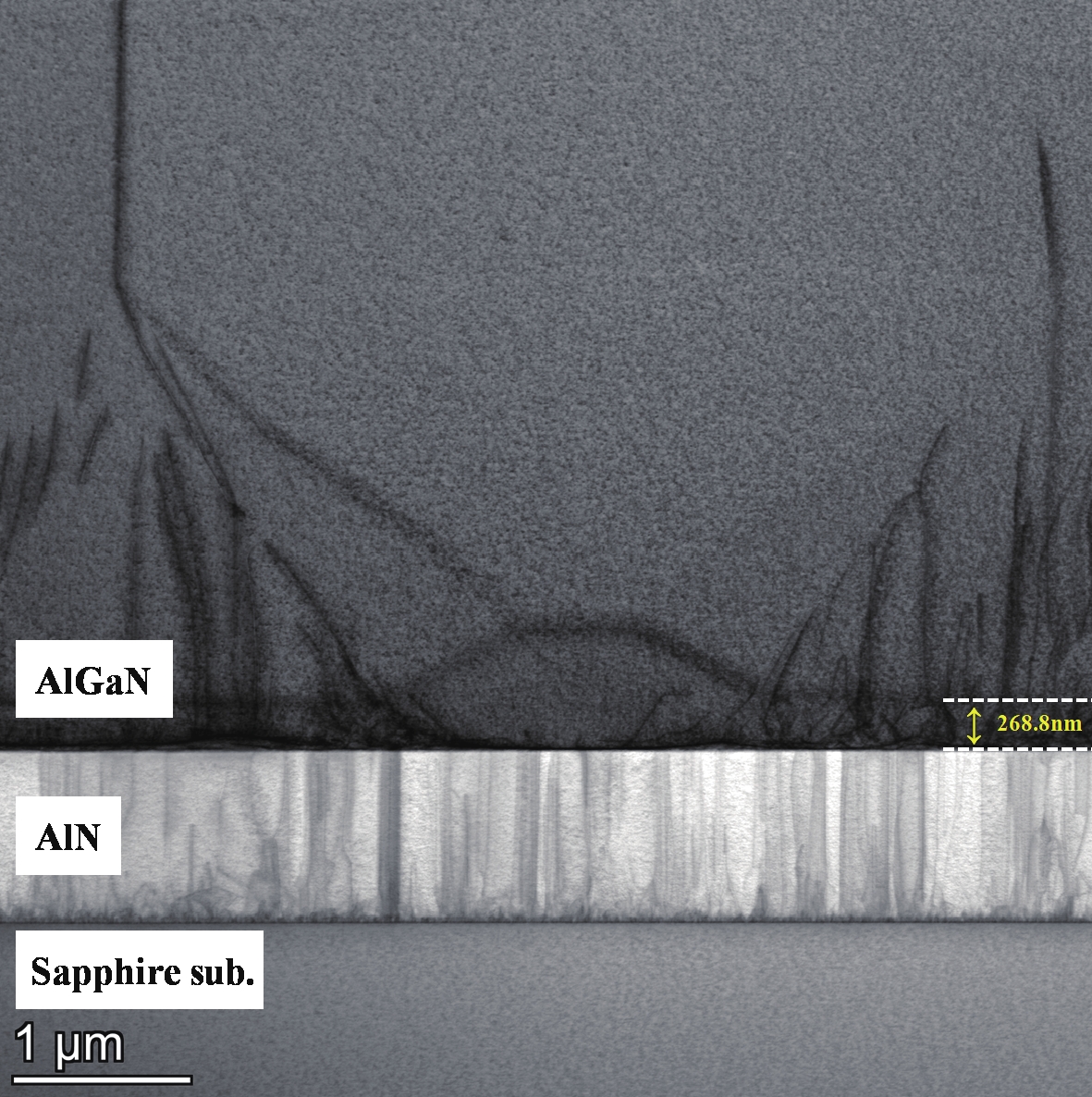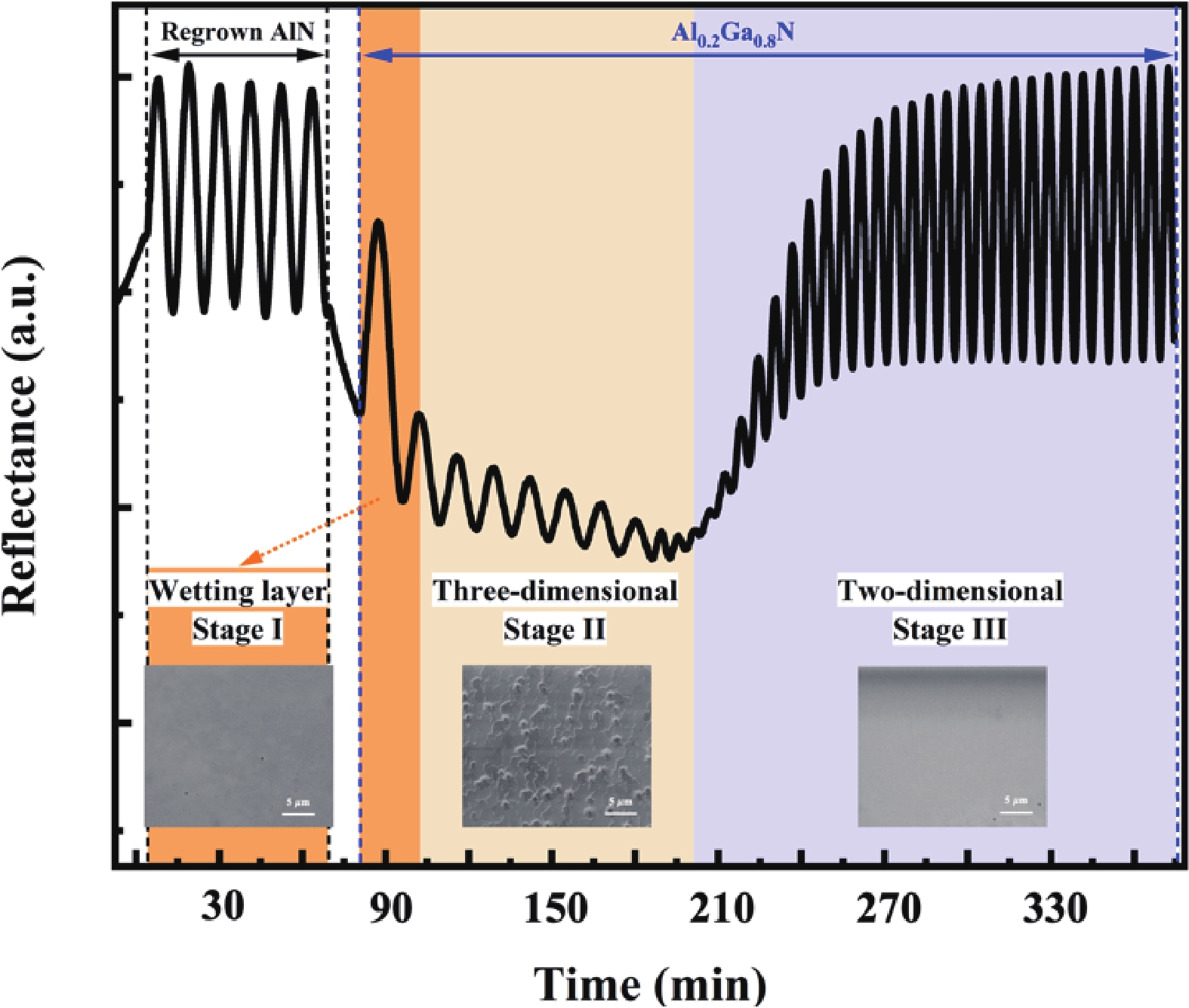
Fig. 1.
(Color online) Measurement results of reflectance intensities by in situ observation of 5 μm Al0.2Ga0.8N using Two-step growth method
ARTICLES
Yaqin Li1, 2, 3, Jianping Liu1, 2, 3, , Aiqin Tian2, 3, , Masao Ikeda2, 3, Wei Zhou2, 3 and Hui Yang1, 2, 3
Corresponding author: Jianping Liu, jpliu2010@sinano.ac.cn; Aiqin Tian, aqtian2012@sinano.ac.cn
Abstract: AlGaN-based ultraviolet (UV) laser diodes (LDs), with emission wavelength in the 280–365 nm range, are promising for applications in medical diagnostics and biological sensing, making them a prominent research focus in both academia and industry in recent years. A key challenge in their development is the large stress induced during the epitaxial growth of LD structures, which arises from the lack of lattice-matched substrates, and severely degrades the quantum efficiency and overall LD performance. This study presents an in-depth investigation into the growth mode and stress evolution of thick Al0.2Ga0.8N template. Firstly, we used the compressive stress between the Al0.2Ga0.8N layer and AlN/Sapphire substrate to form spontaneously three-dimensional growth to annihilate dislocations. Secondly, based on the Nakajima's theory of elasticity, we refined the conventional theoretical models for AlGaN strain relaxation of the S-K growth mode and critical thickness by considering the crucial role of threading dislocations (TDs) in releasing compressive stress. The experimentally measured critical thickness for three-dimensional growth was consistent with the calculated results. Furthermore, a crack-free high-quality 5 μm-thick Al0.2Ga0.8N template was successfully grown on an AlN/sapphire substrate.
Keywords: ultraviolet lasers, strain relaxation, critical thickness
| [1] |
Kneissl M, Rass J. III-Nitride Ultraviolet Emitters: Technology and Applications. Cham: Springer International Publishing, 2016
|
| [2] |
Hargis P J Jr, Sobering T J, Tisone G C, et al. Ultraviolet fluorescence identification of protein, DNA, and bacteria. Opt Instrum Gas Emiss Monit Atmos Meas, 1995, 2366: 147 doi: 10.1117/12.205554
|
| [3] |
Xie N, Xu F J, Wang J M, et al. Stress evolution in AlN growth on nano-patterned sapphire substrates. Appl Phys Express, 2020, 13(1): 015504 doi: 10.7567/1882-0786/ab582c
|
| [4] |
Hagedorn S, Mogilatenko A, Walde S, et al. High-temperature annealing and patterned AlN/sapphire interfaces. Phys Status Solidi B:, 2021, 258(10): 2100187 doi: 10.1002/pssb.202100187
|
| [5] |
Uesugi K, Miyake H. Fabrication of AlN templates by high-temperature face-to-face annealing for deep UV LEDs. Jpn J Appl Phys, 2021, 60(12): 120502 doi: 10.35848/1347-4065/ac3026
|
| [6] |
Uesugi K, Kuboya S, Shojiki K, et al. 263 nm wavelength UV-C LED on face-to-face annealed sputter-deposited AlN with low screw- and mixed-type dislocation densities. Appl Phys Express, 2022, 15(5): 055501 doi: 10.35848/1882-0786/ac66c2
|
| [7] |
Lu S P, Ben J W, Jiang K, et al. 6-inch AlN epitaxial films with low dislocation densities via MOCVD. J Semicond, 2025, 46(2): 022501 doi: 10.1088/1674-4926/24110030
|
| [8] |
Amano H, Collazo R, De Santi C, et al. The 2020 UV emitter roadmap. J Phys D: Appl Phys, 2020, 53(50): 503001 doi: 10.1088/1361-6463/aba64c
|
| [9] |
Bryan I, Bryan Z, Mita S, et al. The role of surface kinetics on composition and quality of AlGaN. J Cryst Growth, 2016, 451: 65 doi: 10.1016/j.jcrysgro.2016.06.055
|
| [10] |
Sato K, Yasue S, Yamada K, et al. Room-temperature operation of AlGaN ultraviolet-B laser diode at 298 nm on lattice-relaxed Al0.6Ga0.4N/AlN/sapphire. Appl Phys Express, 2020, 13(3): 031004
|
| [11] |
Fischer A, Kühne H, Richter H. New approach in equilibrium theory for strained layer relaxation. Phys Rev Lett, 1994, 73(20): 2712 doi: 10.1103/PhysRevLett.73.2712
|
| [12] |
Orr B G, Kessler D, Snyder C W, et al. A model for strain-induced roughening and coherent island growth. Europhys Lett, 1992, 19(1): 33 doi: 10.1209/0295-5075/19/1/006
|
| [13] |
Frank F C, van der Merwe J H. One-dimensional dislocations. I. static theory. Proc R Soc Lond Ser A Math Phys Sci, 1949, 198(1053): 205
|
| [14] |
Volmer M. Nucleus formation in supersaturated systems. Zeitschrift für Physikalische Chemie, 1926, 119: 277
|
| [15] |
Stranski I N, Krastanov L. Theory of orientation separation of ionic crystals. Akad Wiss Let Mainz Math Natur Kl IIb, 1939, 146: 797
|
| [16] |
Nakajima K, Ujihara T, Miyashita S, et al. Effects of misfit dislocations and AlN buffer layer on the GaInN/GaN phase diagram of the growth mode. J Appl Phys, 2001, 89(1): 146 doi: 10.1063/1.1330247
|
| [17] |
Zhao W, Wang L, Wang J X, et al. Theoretical study on critical thicknesses of InGaN grown on (0001) GaN. J Cryst Growth, 2011, 327(1): 202 doi: 10.1016/j.jcrysgro.2011.05.002
|
| [18] |
Harutyunyan V S, Aivazyan A P, Weber E R, et al. High-resolution X-ray diffraction strain-stress analysis of GaN/sapphire heterostructures. J Phys D: Appl Phys, 2001, 34(10A): A35 doi: 10.1088/0022-3727/34/10A/308
|
| [19] |
Huang S Y, Yang J R. A transmission electron microscopy observation of dislocations in GaN grown on (0001) sapphire by metal organic chemical vapor deposition. Jpn J Appl Phys, 2008, 47(10R): 7998 doi: 10.1143/JJAP.47.7998
|
| [20] |
Nakajima K. Equilibrium phase diagrams for stranski-krastanov structure mode of III–V ternary quantum dots. Jpn J Appl Phys, 1999, 38(4R): 1875 doi: 10.1143/JJAP.38.1875
|
| [21] |
Mohamad R, Béré A, Hounkpati V, et al. A theoretical investigation of the miscibility and structural properties of InxAlyGa1−x−yN alloys. Phys Status Solidi B:, 2018, 255(5): 1700394 doi: 10.1002/pssb.201700394
|
| [22] |
Vurgaftman I, Meyer J R. Band parameters for nitrogen-containing semiconductors. J Appl Phys, 2003, 94(6): 3675 doi: 10.1063/1.1600519
|
| [23] |
Sohi P, Martin D, Grandjean N. Critical thickness of GaN on AlN: Impact of growth temperature and dislocation density. Semicond Sci Technol, 2017, 32(7): 075010 doi: 10.1088/1361-6641/aa7248
|
| [24] |
Li Y Q, Tian A Q, Liu J P, et al. Two-step growth of crack-free 5 μm-thick Al0.2Ga0.8N on sapphire substrate with sputtered AlN nucleation layer. J Appl Phys, 2025, 137(6): 065703 doi: 10.1063/5.0249836
|
| [25] |
Iwaya M, Tanaka S, Omori T, et al. Recent development of UV-B laser diodes. Jpn J Appl Phys, 2022, 61(4): 040501 doi: 10.35848/1347-4065/ac3be8
|
Table 1. Parameters used in calculation
| Parameter | AlN | GaN | |
| Lateral lattice constant of a (nm) | 0.3112 | 0.3189 | |
| Young’s modulus ${Y} $ (GPa) | 340 | 329 | |
| Elastic constants Cij | C11/GPa | 396 | 390 |
| C12/GPa | 137 | 145 | |
| C13/GPa | 108 | 106 | |
| C33/GPa | 373 | 398 | |
 DownLoad: CSV
| [1] |
Kneissl M, Rass J. III-Nitride Ultraviolet Emitters: Technology and Applications. Cham: Springer International Publishing, 2016
|
| [2] |
Hargis P J Jr, Sobering T J, Tisone G C, et al. Ultraviolet fluorescence identification of protein, DNA, and bacteria. Opt Instrum Gas Emiss Monit Atmos Meas, 1995, 2366: 147 doi: 10.1117/12.205554
|
| [3] |
Xie N, Xu F J, Wang J M, et al. Stress evolution in AlN growth on nano-patterned sapphire substrates. Appl Phys Express, 2020, 13(1): 015504 doi: 10.7567/1882-0786/ab582c
|
| [4] |
Hagedorn S, Mogilatenko A, Walde S, et al. High-temperature annealing and patterned AlN/sapphire interfaces. Phys Status Solidi B:, 2021, 258(10): 2100187 doi: 10.1002/pssb.202100187
|
| [5] |
Uesugi K, Miyake H. Fabrication of AlN templates by high-temperature face-to-face annealing for deep UV LEDs. Jpn J Appl Phys, 2021, 60(12): 120502 doi: 10.35848/1347-4065/ac3026
|
| [6] |
Uesugi K, Kuboya S, Shojiki K, et al. 263 nm wavelength UV-C LED on face-to-face annealed sputter-deposited AlN with low screw- and mixed-type dislocation densities. Appl Phys Express, 2022, 15(5): 055501 doi: 10.35848/1882-0786/ac66c2
|
| [7] |
Lu S P, Ben J W, Jiang K, et al. 6-inch AlN epitaxial films with low dislocation densities via MOCVD. J Semicond, 2025, 46(2): 022501 doi: 10.1088/1674-4926/24110030
|
| [8] |
Amano H, Collazo R, De Santi C, et al. The 2020 UV emitter roadmap. J Phys D: Appl Phys, 2020, 53(50): 503001 doi: 10.1088/1361-6463/aba64c
|
| [9] |
Bryan I, Bryan Z, Mita S, et al. The role of surface kinetics on composition and quality of AlGaN. J Cryst Growth, 2016, 451: 65 doi: 10.1016/j.jcrysgro.2016.06.055
|
| [10] |
Sato K, Yasue S, Yamada K, et al. Room-temperature operation of AlGaN ultraviolet-B laser diode at 298 nm on lattice-relaxed Al0.6Ga0.4N/AlN/sapphire. Appl Phys Express, 2020, 13(3): 031004
|
| [11] |
Fischer A, Kühne H, Richter H. New approach in equilibrium theory for strained layer relaxation. Phys Rev Lett, 1994, 73(20): 2712 doi: 10.1103/PhysRevLett.73.2712
|
| [12] |
Orr B G, Kessler D, Snyder C W, et al. A model for strain-induced roughening and coherent island growth. Europhys Lett, 1992, 19(1): 33 doi: 10.1209/0295-5075/19/1/006
|
| [13] |
Frank F C, van der Merwe J H. One-dimensional dislocations. I. static theory. Proc R Soc Lond Ser A Math Phys Sci, 1949, 198(1053): 205
|
| [14] |
Volmer M. Nucleus formation in supersaturated systems. Zeitschrift für Physikalische Chemie, 1926, 119: 277
|
| [15] |
Stranski I N, Krastanov L. Theory of orientation separation of ionic crystals. Akad Wiss Let Mainz Math Natur Kl IIb, 1939, 146: 797
|
| [16] |
Nakajima K, Ujihara T, Miyashita S, et al. Effects of misfit dislocations and AlN buffer layer on the GaInN/GaN phase diagram of the growth mode. J Appl Phys, 2001, 89(1): 146 doi: 10.1063/1.1330247
|
| [17] |
Zhao W, Wang L, Wang J X, et al. Theoretical study on critical thicknesses of InGaN grown on (0001) GaN. J Cryst Growth, 2011, 327(1): 202 doi: 10.1016/j.jcrysgro.2011.05.002
|
| [18] |
Harutyunyan V S, Aivazyan A P, Weber E R, et al. High-resolution X-ray diffraction strain-stress analysis of GaN/sapphire heterostructures. J Phys D: Appl Phys, 2001, 34(10A): A35 doi: 10.1088/0022-3727/34/10A/308
|
| [19] |
Huang S Y, Yang J R. A transmission electron microscopy observation of dislocations in GaN grown on (0001) sapphire by metal organic chemical vapor deposition. Jpn J Appl Phys, 2008, 47(10R): 7998 doi: 10.1143/JJAP.47.7998
|
| [20] |
Nakajima K. Equilibrium phase diagrams for stranski-krastanov structure mode of III–V ternary quantum dots. Jpn J Appl Phys, 1999, 38(4R): 1875 doi: 10.1143/JJAP.38.1875
|
| [21] |
Mohamad R, Béré A, Hounkpati V, et al. A theoretical investigation of the miscibility and structural properties of InxAlyGa1−x−yN alloys. Phys Status Solidi B:, 2018, 255(5): 1700394 doi: 10.1002/pssb.201700394
|
| [22] |
Vurgaftman I, Meyer J R. Band parameters for nitrogen-containing semiconductors. J Appl Phys, 2003, 94(6): 3675 doi: 10.1063/1.1600519
|
| [23] |
Sohi P, Martin D, Grandjean N. Critical thickness of GaN on AlN: Impact of growth temperature and dislocation density. Semicond Sci Technol, 2017, 32(7): 075010 doi: 10.1088/1361-6641/aa7248
|
| [24] |
Li Y Q, Tian A Q, Liu J P, et al. Two-step growth of crack-free 5 μm-thick Al0.2Ga0.8N on sapphire substrate with sputtered AlN nucleation layer. J Appl Phys, 2025, 137(6): 065703 doi: 10.1063/5.0249836
|
| [25] |
Iwaya M, Tanaka S, Omori T, et al. Recent development of UV-B laser diodes. Jpn J Appl Phys, 2022, 61(4): 040501 doi: 10.35848/1347-4065/ac3be8
|


Article views: 207 Times PDF downloads: 83 Times Cited by: 0 Times
Received: 27 April 2026 Revised: 03 May 2026 Online: Accepted Manuscript: 03 June 2026
| Citation: |
Yaqin Li, Jianping Liu, Aiqin Tian, Masao Ikeda, Wei Zhou, Hui Yang. Research on the critical thickness of Al0.2Ga0.8N template grown on AlN/sapphire substrate[J]. Journal of Semiconductors, 2026, In Press. doi: 10.1088/1674-4926/26030007
****
Y Q Li, J P Liu, A Q Tian, M Ikeda, W Zhou, and H Yang, Research on the critical thickness of Al0.2Ga0.8N template grown on AlN/sapphire substrate[J]. J. Semicond., 2026, accepted doi: 10.1088/1674-4926/26030007

|
 Yaqin Li got her bachelor’s degree in 2016 from Hebei University of Technology. Now she is a doctoral student at University of Science and Technology of China under the supervision of Prof. Jianping Liu. Her research focuses on MOCVD growth and GaN-Based Laser Diodes
 Jianping Liu got his doctoral degree in 2004 from Institute of Semiconductors, Chinese Academy of Sciences. He is currently a Professor with the Suzhou Institute of Nano-Tech and Nano-Bionics, Chinese Academy of Sciences. His current research interests include GaN-based materials and devices, and MOCVD technology
 Aiqin Tian got her doctoral degree in 2017 from University of Chinese Academy of Sciences. She is currently a Professor with the Suzhou Institute of Nano-Tech and Nano-Bionics, Chinese Academy of Sciences. Her research focuses on GaN-based optoelectronic materials and devices
| [1] |
Kneissl M, Rass J. III-Nitride Ultraviolet Emitters: Technology and Applications. Cham: Springer International Publishing, 2016
|
| [2] |
Hargis P J Jr, Sobering T J, Tisone G C, et al. Ultraviolet fluorescence identification of protein, DNA, and bacteria. Opt Instrum Gas Emiss Monit Atmos Meas, 1995, 2366: 147 doi: 10.1117/12.205554
|
| [3] |
Xie N, Xu F J, Wang J M, et al. Stress evolution in AlN growth on nano-patterned sapphire substrates. Appl Phys Express, 2020, 13(1): 015504 doi: 10.7567/1882-0786/ab582c
|
| [4] |
Hagedorn S, Mogilatenko A, Walde S, et al. High-temperature annealing and patterned AlN/sapphire interfaces. Phys Status Solidi B:, 2021, 258(10): 2100187 doi: 10.1002/pssb.202100187
|
| [5] |
Uesugi K, Miyake H. Fabrication of AlN templates by high-temperature face-to-face annealing for deep UV LEDs. Jpn J Appl Phys, 2021, 60(12): 120502 doi: 10.35848/1347-4065/ac3026
|
| [6] |
Uesugi K, Kuboya S, Shojiki K, et al. 263 nm wavelength UV-C LED on face-to-face annealed sputter-deposited AlN with low screw- and mixed-type dislocation densities. Appl Phys Express, 2022, 15(5): 055501 doi: 10.35848/1882-0786/ac66c2
|
| [7] |
Lu S P, Ben J W, Jiang K, et al. 6-inch AlN epitaxial films with low dislocation densities via MOCVD. J Semicond, 2025, 46(2): 022501 doi: 10.1088/1674-4926/24110030
|
| [8] |
Amano H, Collazo R, De Santi C, et al. The 2020 UV emitter roadmap. J Phys D: Appl Phys, 2020, 53(50): 503001 doi: 10.1088/1361-6463/aba64c
|
| [9] |
Bryan I, Bryan Z, Mita S, et al. The role of surface kinetics on composition and quality of AlGaN. J Cryst Growth, 2016, 451: 65 doi: 10.1016/j.jcrysgro.2016.06.055
|
| [10] |
Sato K, Yasue S, Yamada K, et al. Room-temperature operation of AlGaN ultraviolet-B laser diode at 298 nm on lattice-relaxed Al0.6Ga0.4N/AlN/sapphire. Appl Phys Express, 2020, 13(3): 031004
|
| [11] |
Fischer A, Kühne H, Richter H. New approach in equilibrium theory for strained layer relaxation. Phys Rev Lett, 1994, 73(20): 2712 doi: 10.1103/PhysRevLett.73.2712
|
| [12] |
Orr B G, Kessler D, Snyder C W, et al. A model for strain-induced roughening and coherent island growth. Europhys Lett, 1992, 19(1): 33 doi: 10.1209/0295-5075/19/1/006
|
| [13] |
Frank F C, van der Merwe J H. One-dimensional dislocations. I. static theory. Proc R Soc Lond Ser A Math Phys Sci, 1949, 198(1053): 205
|
| [14] |
Volmer M. Nucleus formation in supersaturated systems. Zeitschrift für Physikalische Chemie, 1926, 119: 277
|
| [15] |
Stranski I N, Krastanov L. Theory of orientation separation of ionic crystals. Akad Wiss Let Mainz Math Natur Kl IIb, 1939, 146: 797
|
| [16] |
Nakajima K, Ujihara T, Miyashita S, et al. Effects of misfit dislocations and AlN buffer layer on the GaInN/GaN phase diagram of the growth mode. J Appl Phys, 2001, 89(1): 146 doi: 10.1063/1.1330247
|
| [17] |
Zhao W, Wang L, Wang J X, et al. Theoretical study on critical thicknesses of InGaN grown on (0001) GaN. J Cryst Growth, 2011, 327(1): 202 doi: 10.1016/j.jcrysgro.2011.05.002
|
| [18] |
Harutyunyan V S, Aivazyan A P, Weber E R, et al. High-resolution X-ray diffraction strain-stress analysis of GaN/sapphire heterostructures. J Phys D: Appl Phys, 2001, 34(10A): A35 doi: 10.1088/0022-3727/34/10A/308
|
| [19] |
Huang S Y, Yang J R. A transmission electron microscopy observation of dislocations in GaN grown on (0001) sapphire by metal organic chemical vapor deposition. Jpn J Appl Phys, 2008, 47(10R): 7998 doi: 10.1143/JJAP.47.7998
|
| [20] |
Nakajima K. Equilibrium phase diagrams for stranski-krastanov structure mode of III–V ternary quantum dots. Jpn J Appl Phys, 1999, 38(4R): 1875 doi: 10.1143/JJAP.38.1875
|
| [21] |
Mohamad R, Béré A, Hounkpati V, et al. A theoretical investigation of the miscibility and structural properties of InxAlyGa1−x−yN alloys. Phys Status Solidi B:, 2018, 255(5): 1700394 doi: 10.1002/pssb.201700394
|
| [22] |
Vurgaftman I, Meyer J R. Band parameters for nitrogen-containing semiconductors. J Appl Phys, 2003, 94(6): 3675 doi: 10.1063/1.1600519
|
| [23] |
Sohi P, Martin D, Grandjean N. Critical thickness of GaN on AlN: Impact of growth temperature and dislocation density. Semicond Sci Technol, 2017, 32(7): 075010 doi: 10.1088/1361-6641/aa7248
|
| [24] |
Li Y Q, Tian A Q, Liu J P, et al. Two-step growth of crack-free 5 μm-thick Al0.2Ga0.8N on sapphire substrate with sputtered AlN nucleation layer. J Appl Phys, 2025, 137(6): 065703 doi: 10.1063/5.0249836
|
| [25] |
Iwaya M, Tanaka S, Omori T, et al. Recent development of UV-B laser diodes. Jpn J Appl Phys, 2022, 61(4): 040501 doi: 10.35848/1347-4065/ac3be8
|
 26030007_Supplementary Information.pdf
|

|

 WeChat ID
Journal of Semiconductors © 2017 All Rights Reserved 京ICP备05085259号-2