


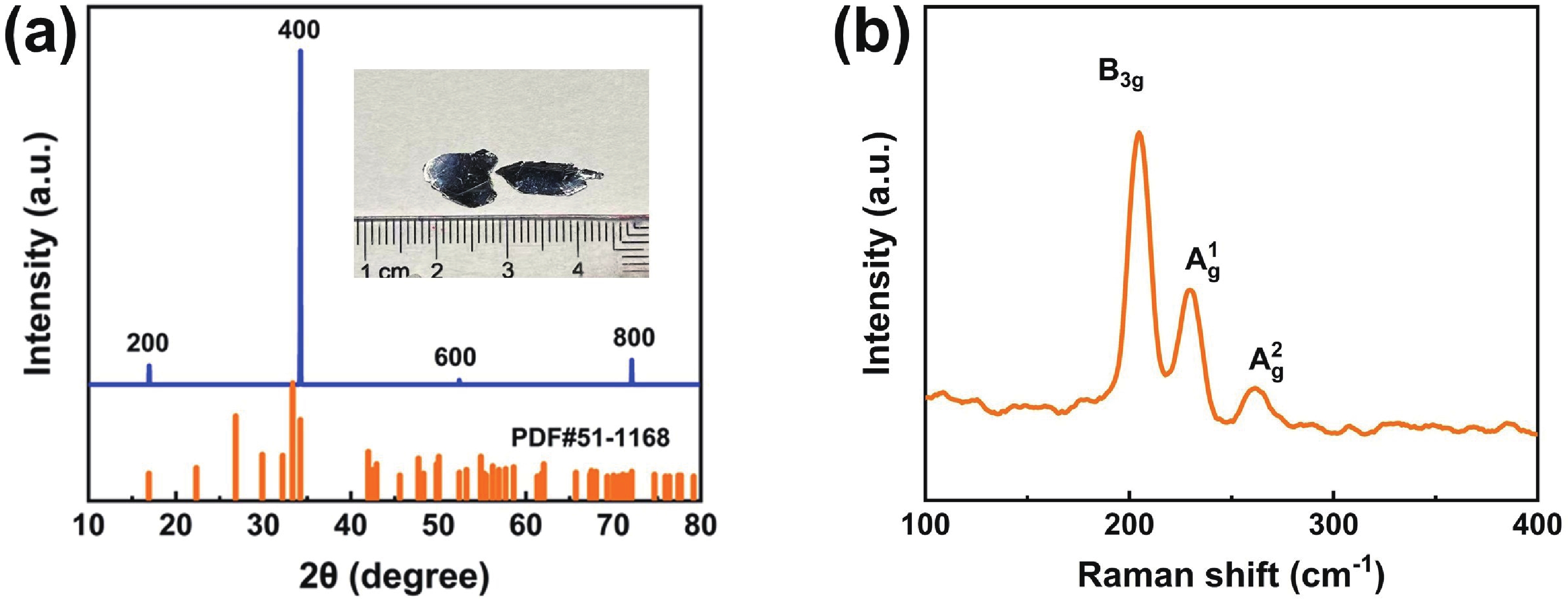
Fig. 1.
(Color online) Characterization of the GeS single crystal. (a) XRD pattern of the GeS single crystal. The inset is the optical image of the GeS single crystal. (b) Raman spectrum of a multilayer GeS nanoflake.
ARTICLES
Xiaoxiang Wu1, Xinyu Zhang1, Yi Zhang1, Peng Li1, Yu Wang1, Yali Liu3, Mengge Li7, Yuyin Li1, Zhanjie Qiu4, Zhengyang Zhanyi4, Songlin Zhou1, 3, Zhongliang Wang1, 6, and Yewu Wang4, 5,
Corresponding author: Zhongliang Wang, guangdianzi_wzl@163.com; Yewu Wang, yewuwang@zju.edu.cn
Abstract: van der Waals (vdW) heterojunctions possess great potential for next-generation high-performance optoelectronic devices owing to their facile fabrication and high-quality interfaces. In this study, GeS/MoS2 vdW heterojunction photodetectors were fabricated and investigated. After suppressing electron recombination by eliminating the non-heterojunction regions on the GeS side, the devices exhibited pronounced rectifying behavior. A large rectification ratio of 2.4×10³ and an ideality factor of 2.3 were achieved. Furthermore, the devices demonstrated photovoltaic-type photodetection performance, including a responsivity of 10.6 mA/W, fast rise/decay time of 83 ms/98 ms, respectively. Notably, the responsivity was further improved to 291.5 mA/W under modulation of Vg. These results provide valuable insights into the optimization and development of high-performance optoelectronic devices based on two-dimensional materials and vdW heterojunctions.
Keywords: two-dimensional materials, MoS2, GeS, van der Waals heterojunction, photodetector.
| [1] |
Moon J H, Nam S, Kim S, et al. Scalable fabrication of mid-wavelength and long-wavelength infrared photodetectors based on narrow bandgap semiconductors: Challenges and opportunities. Int J Extreme Manuf, 2026, 8(1): 012012 doi: 10.1088/2631-7990/ae0100
|
| [2] |
Zou Z X, Liang J W, Zhang X H, et al. Liquid-metal-assisted growth of vertical GaSe/MoS2 p–n heterojunctions for sensitive self-driven photodetectors. ACS Nano, 2021, 15(6): 10039 doi: 10.1021/acsnano.1c01643
|
| [3] |
Zhang Z, Tian Q J, Huo S D, et al. Photodoping strategies in two-dimensional semiconductors: Mechanisms, characterizations, and emerging applications. InfoMat, 2025, 7(12): e70092 doi: 10.1002/inf2.70092
|
| [4] |
Pan X Y, Qu H Y, Shi K X, et al. Defects in 2D layered TMDCs materials: Influence on photoelectric properties and their applications. J Alloys Compd, 2025, 1043: 184196 doi: 10.1016/j.jallcom.2025.184196
|
| [5] |
Yue Y, University F, et al. Multifunctional integrated biosensors based on two-dimensional field-effect transistors. ACS Appl Mater Interfaces, 2024, 16(51): 70160 doi: 10.1021/acsami.4c18412
|
| [6] |
Yoon H H, Park J Y, Megra Y T, et al. Enabling the Angstrom Era: 2D material-based multi-bridge-channel complementary field effect transistors. npj 2D Mater Appl, 2025, 9: 68 doi: 10.1038/s41699-025-00591-z
|
| [7] |
Mitta S B, Choi M S, Nipane A, et al. Electrical characterization of 2D materials-based field-effect transistors. 2D Mater, 2021, 8(1): 012002
|
| [8] |
Wang J, Han J Y, Chen X Q, et al. Design strategies for two-dimensional material photodetectors to enhance device performance. InfoMat, 2019, 1(1): 33 doi: 10.1002/inf2.12004
|
| [9] |
Rezaei M, Bianconi S, Lauhon L J, et al. A new approach to designing high-sensitivity low-dimensional photodetectors. Nano Lett, 2021, 21(23): 9838 doi: 10.1021/acs.nanolett.1c03665
|
| [10] |
Zhong F, Wang H, Wang Z, et al. Recent progress and challenges on two-dimensional material photodetectors from the perspective of advanced characterization technologies. Nano Res, 2021, 14(6): 1840 doi: 10.1007/s12274-020-3247-1
|
| [11] |
Zhou H B, Li S F, Ang K W, et al. Recent advances in in-memory computing: Exploring memristor and memtransistor arrays with 2D materials. Nano Micro Lett, 2024, 16(1): 121 doi: 10.1007/s40820-024-01335-2
|
| [12] |
Ramos M, Gadea M, Mañas-Valero S, et al. Tunable, multifunctional opto-electrical response in multilayer FePS3/single-layer MoS2van der Waals p–n heterojunctions. Nanoscale Adv, 2024, 6(7): 1909 doi: 10.1039/D3NA01134H
|
| [13] |
Duan J M, Chava P, Ghorbani-Asl M, et al. Enhanced trion emission in monolayer MoSe2 by constructing a type-I van der Waals heterostructure. Adv Funct Mater, 2021, 31(40): 2104960 doi: 10.1002/adfm.202104960
|
| [14] |
Duan J M, Chava P, Ghorbani-Asl M, et al. Self-driven broadband photodetectors based on MoSe2/FePS3 van der Waals n–p type-II heterostructures. ACS Appl Mater Interfaces, 2022, 14(9): 11927 doi: 10.1021/acsami.1c24308
|
| [15] |
Cao X Y, Yan S H, Li Z T, et al. Broadband photodetector based on FePS3/WS2 van der Waals type II heterostructure. J Phys Chem Lett, 2023, 14(50): 11529 doi: 10.1021/acs.jpclett.3c03198
|
| [16] |
Tang X, Jiang H S, Lin Z L, et al. Wafer-scale vertical 1D GaN nanorods/2D MoS2/PEDOT: PSS for piezophototronic effect-enhanced self-powered flexible photodetectors. Nano Micro Lett, 2024, 17(1): 56 doi: 10.1007/s40820-024-01553-8
|
| [17] |
Li X, Li Z Q, Hu J H, et al. Tunneling-barrier-controlled sensitive deep ultraviolet photodetectors based on van der Waals heterostructures. Nat Commun, 2025, 16: 2209 doi: 10.1038/s41467-025-56886-8
|
| [18] |
Li J X, Chen J R, He Y X, et al. Controllable growth of monocrystalline MoS2/polycrystalline ReS2 lateral heterojunction for high quantum efficiency photodetector. Adv Funct Mater, 2025, 35(27): 2421508 doi: 10.1002/adfm.202421508
|
| [19] |
Ouyang Y, Zhang C Y, Wang J, et al. Gate-tunable dual-mode optoelectronic device for self-powered photodetector and optoelectronic synapse. Adv Sci, 2025, 12(17): 2416259 doi: 10.1002/advs.202416259
|
| [20] |
Dutta R, Bala A, Sen A, et al. Optical enhancement of indirect bandgap 2D transition metal dichalcogenides for multi-functional optoelectronic sensors. Adv Mater, 2023, 35(46): 2303272 doi: 10.1002/adma.202303272
|
| [21] |
Mohammadzadeh M R, Hasani A, Jaferzadeh K, et al. Unique photoactivated time-resolved response in 2D GeS for selective detection of volatile organic compounds. Adv Sci, 2023, 10(10): 2205458 doi: 10.1002/advs.202205458
|
| [22] |
Liu Y, Huang Y, Duan X F. Van der Waals integration before and beyond two-dimensional materials. Nature, 2019, 567(7748): 323 doi: 10.1038/s41586-019-1013-x
|
| [23] |
Sutter E, Zhang B, Sun M H, et al. Few-layer to multilayer germanium(II) sulfide: Synthesis, structure, stability, and optoelectronics. ACS Nano, 2019, 13(8): 9352 doi: 10.1021/acsnano.9b03986
|
| [24] |
Ho C H, Li J X. Polarized band-edge emission and dichroic optical behavior in thin multilayer GeS. Adv Opt Mater, 2017, 5(3): 1600814 doi: 10.1002/adom.201600814
|
| [25] |
Tan D Z, Lim H E, Wang F J, et al. Anisotropic optical and electronic properties of two-dimensional layered germanium sulfide. Nano Res, 2017, 10(2): 546 doi: 10.1007/s12274-016-1312-6
|
| [26] |
Ulaganathan R K, Lu Y-Y, Kuo C J, et al. High photosensitivity and broad spectral response of multi-layered germanium sulfide transistors. Nanoscale, 2016, 8(4): 2284 doi: 10.1039/C5NR05988G
|
| [27] |
Lan C Y, Li C, Yin Y, et al. Synthesis of single-crystalline GeS nanoribbons for high sensitivity visible-light photodetectors. J Mater Chem C, 2015, 3(31): 8074 doi: 10.1039/C5TC01435B
|
| [28] |
Li N, He C L, Wang Q Q, et al. Gate-tunable large-scale flexible monolayer MoS2 devices for photodetectors and optoelectronic synapses. Nano Res, 2022, 15(6): 5418 doi: 10.1007/s12274-022-4122-z
|
| [29] |
Thayil R, Parne S R, Ramana C V. 2D MoS2 for next-generation electronics and optoelectronics: From material properties to manufacturing challenges and future prospects. Small, 2025, 21(14): 2412467 doi: 10.1002/smll.202412467
|
| [30] |
Wang F, Wang Z X, Xu K, et al. Tunable GaTe-MoS2 van der Waals p–n junctions with novel optoelectronic performance. Nano Lett, 2015, 15(11): 7558 doi: 10.1021/acs.nanolett.5b03291
|
| [31] |
Yang S X, Wang C, Ataca C, et al. Self-Driven Photodetector and Ambipolar Transistor in Atomically Thin GaTe-MoS2 p–n vdW Heterostructure. ACS Appl Mater Interfaces, 2016, 8(4): 2533 doi: 10.1021/acsami.5b10001
|
| [32] |
Khan M A, Rathi S, Lim D, et al. Gate tunable self-biased diode based on few layered MoS2 and WSe2. Chem Mater, 2018, 30(3): 1011 doi: 10.1021/acs.chemmater.7b04865
|
| [33] |
Bong H, Kwon G, Choe J, et al. Ultrasensitive and spectrally selective WSe2/MoS2 photodetector via metal–2D interface modulation for infrared signal recognition. InfoMat, 2025, 7(12): e70065 doi: 10.1002/inf2.70065
|
| [34] |
Xiao H D, Lin L, Zhu J, et al. Highly sensitive and broadband photodetectors based on WSe2/MoS2 heterostructures with van der Waals contact electrodes. Appl Phys Lett, 2022, 121(2): 023504 doi: 10.1063/5.0100191
|
| [35] |
Paul Inbaraj C R, Mathew R J, Ulaganathan R K, et al. Modulating charge separation with hexagonal boron nitride mediation in vertical van der Waals heterostructures. ACS Appl Mater Interfaces, 2020, 12(23): 26213 doi: 10.1021/acsami.0c06077
|
| [36] |
He Z B, Guo J X, Li S D, et al. GaSe/MoS2 heterostructure with ohmic-contact electrodes for fast, broadband photoresponse, and self-driven photodetectors. Adv Mater Interfaces, 2020, 7(9): 1901848 doi: 10.1002/admi.201901848
|
| [37] |
Paramanik R, Kundu T, Das S, et al. In-plane anisotropy-driven directional charge transport in van der Waals p–n heterojunctions. Nanoscale, 2025, 17(41): 24121 doi: 10.1039/D5NR02390D
|
| [38] |
Lei T, Lü W-M, Lü W-X, et al. Photogating effect in two-dimensional photodetectors. Acta Phys Sin, 2021, 70(2): 027801
|
| [39] |
Shin G H, Park C, Lee K J, et al. Ultrasensitive phototransistor based on WSe2–MoS2 van der Waals heterojunction. Nano Lett, 2020, 20(8): 5741 doi: 10.1021/acs.nanolett.0c01460
|
| [40] |
Liu Y L, Wu X X, Guo W X, et al. Enhanced performance of a n-Si/p-GaTe heterojunction through interfacial passivation and thermal oxidation. J Mater Chem C, 2022, 10(32): 11747 doi: 10.1039/D2TC02740B
|
| [41] |
Chen P, Atallah T L, Lin Z Y, et al. Approaching the intrinsic exciton physics limit in two-dimensional semiconductor diodes. Nature, 2021, 599(7885): 404 doi: 10.1038/s41586-021-03949-7
|
| [42] |
Wu X X, Xiao C, Wang Y, et al. Self-driven high-performance gate-voltage-tunable and enhanced performance optoelectronic device based on FePS3/MoS2 heterojunctions. ACS Appl Mater Interfaces, 2025, 17(12): 18601 doi: 10.1021/acsami.4c22204
|
| [43] |
Zhang N, Wu L W, Gao W, et al. Near-infrared, self-powered and polarization-sensitive photodetector based on GeSe–MoTe2 p–n heterojunction. Adv Mater Interfaces, 2022, 9(15): 2200150 doi: 10.1002/admi.202200150
|
| [44] |
Xu Y H, Wang Y X, Zhang C C, et al. The role of trap states in MoS2-based photodetectors. Nanoscale, 2025, 17(15): 9245 doi: 10.1039/D4NR04974H
|
| [45] |
Zhang Y W, Ma K K, Zhao C, et al. An ultrafast WSe2 photodiode based on a lateral p-i-n homojunction. ACS Nano, 2021, 15(3): 4405 doi: 10.1021/acsnano.0c08075
|
| [46] |
Wu D, Guo J W, Du J, et al. Highly polarization-sensitive, broadband, self-powered photodetector based on graphene/PdSe2/germanium heterojunction. ACS Nano, 2019, 13(9): 9907 doi: 10.1021/acsnano.9b03994
|
| [47] |
Cao Z Y, Ni K P, Zhou J Y, et al. Gate modulated high-performance polarization-sensitive photodiode based on WSe2/Ta2Pd3Se8 hybrid dimensional heterostructure. Adv Opt Mater, 2025, 13(18): 2500340 doi: 10.1002/adom.202500340
|
| [48] |
Ahn J, Kyhm J H, Kang H K, et al. 2D MoTe2/ReS2 van der Waals heterostructure for high-performance and linear polarization-sensitive photodetector. ACS Photonics, 2021, 8(9): 2650 doi: 10.1021/acsphotonics.1c00598
|
| [49] |
Dai T F, Zhang Y, Wang F K, et al. Broadband mid-infrared polarization-sensitive photodetection based on BP/Ta2NiS5 heterojunction. Adv Opt Mater, 2025, 13(25): e01297 doi: 10.1002/adom.202501297
|
| [50] |
Fang Y J, Armin A, Meredith P, et al. Accurate characterization of next-generation thin-film photodetectors. Nat Photonics, 2019, 13(1): 1 doi: 10.1038/s41566-018-0288-z
|
| [51] |
Xu X B, Chen J C, et al. Van der Waals complementary barrier infrared detector. ACS Nano, 2025, 19(19): 18747 doi: 10.1021/acsnano.5c03529
|
| [52] |
Zheng T, Yang M M, Pan Y, et al. Self-powered photodetector with high efficiency and polarization sensitivity enabled by WSe2/Ta2NiSe5/WSe2 van der Waals dual heterojunction. ACS Appl Mater Interfaces, 2023, 15(24): 29363 doi: 10.1021/acsami.3c04147
|
| [53] |
Yang J J, Song J M, Zhao X, et al. Visible-light self-powered photodetector with high sensitivity based on the type-II heterostructure of CdPSe3/MoS2. ACS Appl Mater Interfaces, 2024, 16(25): 32334 doi: 10.1021/acsami.4c01183
|
| [54] |
Yang S, Liu Y J, Wu Y P, et al. High-performance flexible photodetectors based on CdTe/MoS2heterojunction. Nanoscale, 2024, 16(29): 13932 doi: 10.1039/D4NR01718H
|
Table 1. Performance comparison between our GeS/MoS2 vdW heterojunction-based photodetectors and other devices in literatures.
| Heterojunctions | Rectification ratio | Ideality factor | External bias (V) | R(mA/W) | rise/decay time | Refs |
| FePS3/WS2 | — | — | –2 | 32.5 | 220/160 ms | [15] |
| FePS3/MoSe2 | 18 | 2.7 | 0 | 52 | 600/600 ms | [14] |
| InSe/GeS | 7 | — | 5 | 2.7×10⁵ | — | [35] |
| CdPSe3/MoS2 | — | — | 5 | 91.12 | 27/20 ms | [53] |
| CdTe/MoS2 | 46.3 | — | 0 | 270.3 | 44.8/134.2 μs. | [54] |
| GeS/MoS2 | ~102 | — | -2 | 21 | — | [37] |
| GeS/MoS2 | 2.4×10³ | 2.3 | 0 | 10.6 | 83/98 ms | This work |
| –1 (Vg = 40 V) | 291.5 | 52.6/49.2 ms |
 DownLoad: CSV
| [1] |
Moon J H, Nam S, Kim S, et al. Scalable fabrication of mid-wavelength and long-wavelength infrared photodetectors based on narrow bandgap semiconductors: Challenges and opportunities. Int J Extreme Manuf, 2026, 8(1): 012012 doi: 10.1088/2631-7990/ae0100
|
| [2] |
Zou Z X, Liang J W, Zhang X H, et al. Liquid-metal-assisted growth of vertical GaSe/MoS2 p–n heterojunctions for sensitive self-driven photodetectors. ACS Nano, 2021, 15(6): 10039 doi: 10.1021/acsnano.1c01643
|
| [3] |
Zhang Z, Tian Q J, Huo S D, et al. Photodoping strategies in two-dimensional semiconductors: Mechanisms, characterizations, and emerging applications. InfoMat, 2025, 7(12): e70092 doi: 10.1002/inf2.70092
|
| [4] |
Pan X Y, Qu H Y, Shi K X, et al. Defects in 2D layered TMDCs materials: Influence on photoelectric properties and their applications. J Alloys Compd, 2025, 1043: 184196 doi: 10.1016/j.jallcom.2025.184196
|
| [5] |
Yue Y, University F, et al. Multifunctional integrated biosensors based on two-dimensional field-effect transistors. ACS Appl Mater Interfaces, 2024, 16(51): 70160 doi: 10.1021/acsami.4c18412
|
| [6] |
Yoon H H, Park J Y, Megra Y T, et al. Enabling the Angstrom Era: 2D material-based multi-bridge-channel complementary field effect transistors. npj 2D Mater Appl, 2025, 9: 68 doi: 10.1038/s41699-025-00591-z
|
| [7] |
Mitta S B, Choi M S, Nipane A, et al. Electrical characterization of 2D materials-based field-effect transistors. 2D Mater, 2021, 8(1): 012002
|
| [8] |
Wang J, Han J Y, Chen X Q, et al. Design strategies for two-dimensional material photodetectors to enhance device performance. InfoMat, 2019, 1(1): 33 doi: 10.1002/inf2.12004
|
| [9] |
Rezaei M, Bianconi S, Lauhon L J, et al. A new approach to designing high-sensitivity low-dimensional photodetectors. Nano Lett, 2021, 21(23): 9838 doi: 10.1021/acs.nanolett.1c03665
|
| [10] |
Zhong F, Wang H, Wang Z, et al. Recent progress and challenges on two-dimensional material photodetectors from the perspective of advanced characterization technologies. Nano Res, 2021, 14(6): 1840 doi: 10.1007/s12274-020-3247-1
|
| [11] |
Zhou H B, Li S F, Ang K W, et al. Recent advances in in-memory computing: Exploring memristor and memtransistor arrays with 2D materials. Nano Micro Lett, 2024, 16(1): 121 doi: 10.1007/s40820-024-01335-2
|
| [12] |
Ramos M, Gadea M, Mañas-Valero S, et al. Tunable, multifunctional opto-electrical response in multilayer FePS3/single-layer MoS2van der Waals p–n heterojunctions. Nanoscale Adv, 2024, 6(7): 1909 doi: 10.1039/D3NA01134H
|
| [13] |
Duan J M, Chava P, Ghorbani-Asl M, et al. Enhanced trion emission in monolayer MoSe2 by constructing a type-I van der Waals heterostructure. Adv Funct Mater, 2021, 31(40): 2104960 doi: 10.1002/adfm.202104960
|
| [14] |
Duan J M, Chava P, Ghorbani-Asl M, et al. Self-driven broadband photodetectors based on MoSe2/FePS3 van der Waals n–p type-II heterostructures. ACS Appl Mater Interfaces, 2022, 14(9): 11927 doi: 10.1021/acsami.1c24308
|
| [15] |
Cao X Y, Yan S H, Li Z T, et al. Broadband photodetector based on FePS3/WS2 van der Waals type II heterostructure. J Phys Chem Lett, 2023, 14(50): 11529 doi: 10.1021/acs.jpclett.3c03198
|
| [16] |
Tang X, Jiang H S, Lin Z L, et al. Wafer-scale vertical 1D GaN nanorods/2D MoS2/PEDOT: PSS for piezophototronic effect-enhanced self-powered flexible photodetectors. Nano Micro Lett, 2024, 17(1): 56 doi: 10.1007/s40820-024-01553-8
|
| [17] |
Li X, Li Z Q, Hu J H, et al. Tunneling-barrier-controlled sensitive deep ultraviolet photodetectors based on van der Waals heterostructures. Nat Commun, 2025, 16: 2209 doi: 10.1038/s41467-025-56886-8
|
| [18] |
Li J X, Chen J R, He Y X, et al. Controllable growth of monocrystalline MoS2/polycrystalline ReS2 lateral heterojunction for high quantum efficiency photodetector. Adv Funct Mater, 2025, 35(27): 2421508 doi: 10.1002/adfm.202421508
|
| [19] |
Ouyang Y, Zhang C Y, Wang J, et al. Gate-tunable dual-mode optoelectronic device for self-powered photodetector and optoelectronic synapse. Adv Sci, 2025, 12(17): 2416259 doi: 10.1002/advs.202416259
|
| [20] |
Dutta R, Bala A, Sen A, et al. Optical enhancement of indirect bandgap 2D transition metal dichalcogenides for multi-functional optoelectronic sensors. Adv Mater, 2023, 35(46): 2303272 doi: 10.1002/adma.202303272
|
| [21] |
Mohammadzadeh M R, Hasani A, Jaferzadeh K, et al. Unique photoactivated time-resolved response in 2D GeS for selective detection of volatile organic compounds. Adv Sci, 2023, 10(10): 2205458 doi: 10.1002/advs.202205458
|
| [22] |
Liu Y, Huang Y, Duan X F. Van der Waals integration before and beyond two-dimensional materials. Nature, 2019, 567(7748): 323 doi: 10.1038/s41586-019-1013-x
|
| [23] |
Sutter E, Zhang B, Sun M H, et al. Few-layer to multilayer germanium(II) sulfide: Synthesis, structure, stability, and optoelectronics. ACS Nano, 2019, 13(8): 9352 doi: 10.1021/acsnano.9b03986
|
| [24] |
Ho C H, Li J X. Polarized band-edge emission and dichroic optical behavior in thin multilayer GeS. Adv Opt Mater, 2017, 5(3): 1600814 doi: 10.1002/adom.201600814
|
| [25] |
Tan D Z, Lim H E, Wang F J, et al. Anisotropic optical and electronic properties of two-dimensional layered germanium sulfide. Nano Res, 2017, 10(2): 546 doi: 10.1007/s12274-016-1312-6
|
| [26] |
Ulaganathan R K, Lu Y-Y, Kuo C J, et al. High photosensitivity and broad spectral response of multi-layered germanium sulfide transistors. Nanoscale, 2016, 8(4): 2284 doi: 10.1039/C5NR05988G
|
| [27] |
Lan C Y, Li C, Yin Y, et al. Synthesis of single-crystalline GeS nanoribbons for high sensitivity visible-light photodetectors. J Mater Chem C, 2015, 3(31): 8074 doi: 10.1039/C5TC01435B
|
| [28] |
Li N, He C L, Wang Q Q, et al. Gate-tunable large-scale flexible monolayer MoS2 devices for photodetectors and optoelectronic synapses. Nano Res, 2022, 15(6): 5418 doi: 10.1007/s12274-022-4122-z
|
| [29] |
Thayil R, Parne S R, Ramana C V. 2D MoS2 for next-generation electronics and optoelectronics: From material properties to manufacturing challenges and future prospects. Small, 2025, 21(14): 2412467 doi: 10.1002/smll.202412467
|
| [30] |
Wang F, Wang Z X, Xu K, et al. Tunable GaTe-MoS2 van der Waals p–n junctions with novel optoelectronic performance. Nano Lett, 2015, 15(11): 7558 doi: 10.1021/acs.nanolett.5b03291
|
| [31] |
Yang S X, Wang C, Ataca C, et al. Self-Driven Photodetector and Ambipolar Transistor in Atomically Thin GaTe-MoS2 p–n vdW Heterostructure. ACS Appl Mater Interfaces, 2016, 8(4): 2533 doi: 10.1021/acsami.5b10001
|
| [32] |
Khan M A, Rathi S, Lim D, et al. Gate tunable self-biased diode based on few layered MoS2 and WSe2. Chem Mater, 2018, 30(3): 1011 doi: 10.1021/acs.chemmater.7b04865
|
| [33] |
Bong H, Kwon G, Choe J, et al. Ultrasensitive and spectrally selective WSe2/MoS2 photodetector via metal–2D interface modulation for infrared signal recognition. InfoMat, 2025, 7(12): e70065 doi: 10.1002/inf2.70065
|
| [34] |
Xiao H D, Lin L, Zhu J, et al. Highly sensitive and broadband photodetectors based on WSe2/MoS2 heterostructures with van der Waals contact electrodes. Appl Phys Lett, 2022, 121(2): 023504 doi: 10.1063/5.0100191
|
| [35] |
Paul Inbaraj C R, Mathew R J, Ulaganathan R K, et al. Modulating charge separation with hexagonal boron nitride mediation in vertical van der Waals heterostructures. ACS Appl Mater Interfaces, 2020, 12(23): 26213 doi: 10.1021/acsami.0c06077
|
| [36] |
He Z B, Guo J X, Li S D, et al. GaSe/MoS2 heterostructure with ohmic-contact electrodes for fast, broadband photoresponse, and self-driven photodetectors. Adv Mater Interfaces, 2020, 7(9): 1901848 doi: 10.1002/admi.201901848
|
| [37] |
Paramanik R, Kundu T, Das S, et al. In-plane anisotropy-driven directional charge transport in van der Waals p–n heterojunctions. Nanoscale, 2025, 17(41): 24121 doi: 10.1039/D5NR02390D
|
| [38] |
Lei T, Lü W-M, Lü W-X, et al. Photogating effect in two-dimensional photodetectors. Acta Phys Sin, 2021, 70(2): 027801
|
| [39] |
Shin G H, Park C, Lee K J, et al. Ultrasensitive phototransistor based on WSe2–MoS2 van der Waals heterojunction. Nano Lett, 2020, 20(8): 5741 doi: 10.1021/acs.nanolett.0c01460
|
| [40] |
Liu Y L, Wu X X, Guo W X, et al. Enhanced performance of a n-Si/p-GaTe heterojunction through interfacial passivation and thermal oxidation. J Mater Chem C, 2022, 10(32): 11747 doi: 10.1039/D2TC02740B
|
| [41] |
Chen P, Atallah T L, Lin Z Y, et al. Approaching the intrinsic exciton physics limit in two-dimensional semiconductor diodes. Nature, 2021, 599(7885): 404 doi: 10.1038/s41586-021-03949-7
|
| [42] |
Wu X X, Xiao C, Wang Y, et al. Self-driven high-performance gate-voltage-tunable and enhanced performance optoelectronic device based on FePS3/MoS2 heterojunctions. ACS Appl Mater Interfaces, 2025, 17(12): 18601 doi: 10.1021/acsami.4c22204
|
| [43] |
Zhang N, Wu L W, Gao W, et al. Near-infrared, self-powered and polarization-sensitive photodetector based on GeSe–MoTe2 p–n heterojunction. Adv Mater Interfaces, 2022, 9(15): 2200150 doi: 10.1002/admi.202200150
|
| [44] |
Xu Y H, Wang Y X, Zhang C C, et al. The role of trap states in MoS2-based photodetectors. Nanoscale, 2025, 17(15): 9245 doi: 10.1039/D4NR04974H
|
| [45] |
Zhang Y W, Ma K K, Zhao C, et al. An ultrafast WSe2 photodiode based on a lateral p-i-n homojunction. ACS Nano, 2021, 15(3): 4405 doi: 10.1021/acsnano.0c08075
|
| [46] |
Wu D, Guo J W, Du J, et al. Highly polarization-sensitive, broadband, self-powered photodetector based on graphene/PdSe2/germanium heterojunction. ACS Nano, 2019, 13(9): 9907 doi: 10.1021/acsnano.9b03994
|
| [47] |
Cao Z Y, Ni K P, Zhou J Y, et al. Gate modulated high-performance polarization-sensitive photodiode based on WSe2/Ta2Pd3Se8 hybrid dimensional heterostructure. Adv Opt Mater, 2025, 13(18): 2500340 doi: 10.1002/adom.202500340
|
| [48] |
Ahn J, Kyhm J H, Kang H K, et al. 2D MoTe2/ReS2 van der Waals heterostructure for high-performance and linear polarization-sensitive photodetector. ACS Photonics, 2021, 8(9): 2650 doi: 10.1021/acsphotonics.1c00598
|
| [49] |
Dai T F, Zhang Y, Wang F K, et al. Broadband mid-infrared polarization-sensitive photodetection based on BP/Ta2NiS5 heterojunction. Adv Opt Mater, 2025, 13(25): e01297 doi: 10.1002/adom.202501297
|
| [50] |
Fang Y J, Armin A, Meredith P, et al. Accurate characterization of next-generation thin-film photodetectors. Nat Photonics, 2019, 13(1): 1 doi: 10.1038/s41566-018-0288-z
|
| [51] |
Xu X B, Chen J C, et al. Van der Waals complementary barrier infrared detector. ACS Nano, 2025, 19(19): 18747 doi: 10.1021/acsnano.5c03529
|
| [52] |
Zheng T, Yang M M, Pan Y, et al. Self-powered photodetector with high efficiency and polarization sensitivity enabled by WSe2/Ta2NiSe5/WSe2 van der Waals dual heterojunction. ACS Appl Mater Interfaces, 2023, 15(24): 29363 doi: 10.1021/acsami.3c04147
|
| [53] |
Yang J J, Song J M, Zhao X, et al. Visible-light self-powered photodetector with high sensitivity based on the type-II heterostructure of CdPSe3/MoS2. ACS Appl Mater Interfaces, 2024, 16(25): 32334 doi: 10.1021/acsami.4c01183
|
| [54] |
Yang S, Liu Y J, Wu Y P, et al. High-performance flexible photodetectors based on CdTe/MoS2heterojunction. Nanoscale, 2024, 16(29): 13932 doi: 10.1039/D4NR01718H
|





Article views: 2 Times PDF downloads: 0 Times Cited by: 0 Times
Received: 18 March 2026 Revised: 21 June 2026 Online: Accepted Manuscript: 07 August 2026
| Citation: |
Xiaoxiang Wu, Xinyu Zhang, Yi Zhang, Peng Li, Yu Wang, Yali Liu, Mengge Li, Yuyin Li, Zhanjie Qiu, Zhengyang Zhanyi, Songlin Zhou, Zhongliang Wang, Yewu Wang. Performance enhancement of GeS/MoS2 van der Waals heterojunction optoelectronic device with photovoltaic-type photodetection[J]. Journal of Semiconductors, 2026, In Press. doi: 10.1088/1674-4926/26030026
****
X X Wu, X Y Zhang, Y Zhang, P Li, Y Wang, Y L Liu, M G Li, Y Y Li, Z J Qiu, Z Y Z yi, S L Zhou, Z L Wang, and Y W Wang, Performance enhancement of GeS/MoS2 van der Waals heterojunction optoelectronic device with photovoltaic-type photodetection[J]. J. Semicond., 2026, accepted doi: 10.1088/1674-4926/26030026

|
 Xiaoxiang Wu received his doctoral degree from the School of Physics, Zhejiang University, in 2023. He is currently a Lecturer at the School of Electrical and Information Engineering, Tongling University. His research interests mainly focus on the single-crystal growth of two-dimensional semiconductor materials and the investigation of their optoelectronic device performance
 Zhongliang Wang received his doctoral degree in Information and Communication Engineering from the School of Electronics and Information, Northwestern Polytechnical University. He is currently a Professor at the School of Electrical and Information Engineering, Tongling University. His research interests involve computational imaging and hyperspectral remote sensing image processing
| [1] |
Moon J H, Nam S, Kim S, et al. Scalable fabrication of mid-wavelength and long-wavelength infrared photodetectors based on narrow bandgap semiconductors: Challenges and opportunities. Int J Extreme Manuf, 2026, 8(1): 012012 doi: 10.1088/2631-7990/ae0100
|
| [2] |
Zou Z X, Liang J W, Zhang X H, et al. Liquid-metal-assisted growth of vertical GaSe/MoS2 p–n heterojunctions for sensitive self-driven photodetectors. ACS Nano, 2021, 15(6): 10039 doi: 10.1021/acsnano.1c01643
|
| [3] |
Zhang Z, Tian Q J, Huo S D, et al. Photodoping strategies in two-dimensional semiconductors: Mechanisms, characterizations, and emerging applications. InfoMat, 2025, 7(12): e70092 doi: 10.1002/inf2.70092
|
| [4] |
Pan X Y, Qu H Y, Shi K X, et al. Defects in 2D layered TMDCs materials: Influence on photoelectric properties and their applications. J Alloys Compd, 2025, 1043: 184196 doi: 10.1016/j.jallcom.2025.184196
|
| [5] |
Yue Y, University F, et al. Multifunctional integrated biosensors based on two-dimensional field-effect transistors. ACS Appl Mater Interfaces, 2024, 16(51): 70160 doi: 10.1021/acsami.4c18412
|
| [6] |
Yoon H H, Park J Y, Megra Y T, et al. Enabling the Angstrom Era: 2D material-based multi-bridge-channel complementary field effect transistors. npj 2D Mater Appl, 2025, 9: 68 doi: 10.1038/s41699-025-00591-z
|
| [7] |
Mitta S B, Choi M S, Nipane A, et al. Electrical characterization of 2D materials-based field-effect transistors. 2D Mater, 2021, 8(1): 012002
|
| [8] |
Wang J, Han J Y, Chen X Q, et al. Design strategies for two-dimensional material photodetectors to enhance device performance. InfoMat, 2019, 1(1): 33 doi: 10.1002/inf2.12004
|
| [9] |
Rezaei M, Bianconi S, Lauhon L J, et al. A new approach to designing high-sensitivity low-dimensional photodetectors. Nano Lett, 2021, 21(23): 9838 doi: 10.1021/acs.nanolett.1c03665
|
| [10] |
Zhong F, Wang H, Wang Z, et al. Recent progress and challenges on two-dimensional material photodetectors from the perspective of advanced characterization technologies. Nano Res, 2021, 14(6): 1840 doi: 10.1007/s12274-020-3247-1
|
| [11] |
Zhou H B, Li S F, Ang K W, et al. Recent advances in in-memory computing: Exploring memristor and memtransistor arrays with 2D materials. Nano Micro Lett, 2024, 16(1): 121 doi: 10.1007/s40820-024-01335-2
|
| [12] |
Ramos M, Gadea M, Mañas-Valero S, et al. Tunable, multifunctional opto-electrical response in multilayer FePS3/single-layer MoS2van der Waals p–n heterojunctions. Nanoscale Adv, 2024, 6(7): 1909 doi: 10.1039/D3NA01134H
|
| [13] |
Duan J M, Chava P, Ghorbani-Asl M, et al. Enhanced trion emission in monolayer MoSe2 by constructing a type-I van der Waals heterostructure. Adv Funct Mater, 2021, 31(40): 2104960 doi: 10.1002/adfm.202104960
|
| [14] |
Duan J M, Chava P, Ghorbani-Asl M, et al. Self-driven broadband photodetectors based on MoSe2/FePS3 van der Waals n–p type-II heterostructures. ACS Appl Mater Interfaces, 2022, 14(9): 11927 doi: 10.1021/acsami.1c24308
|
| [15] |
Cao X Y, Yan S H, Li Z T, et al. Broadband photodetector based on FePS3/WS2 van der Waals type II heterostructure. J Phys Chem Lett, 2023, 14(50): 11529 doi: 10.1021/acs.jpclett.3c03198
|
| [16] |
Tang X, Jiang H S, Lin Z L, et al. Wafer-scale vertical 1D GaN nanorods/2D MoS2/PEDOT: PSS for piezophototronic effect-enhanced self-powered flexible photodetectors. Nano Micro Lett, 2024, 17(1): 56 doi: 10.1007/s40820-024-01553-8
|
| [17] |
Li X, Li Z Q, Hu J H, et al. Tunneling-barrier-controlled sensitive deep ultraviolet photodetectors based on van der Waals heterostructures. Nat Commun, 2025, 16: 2209 doi: 10.1038/s41467-025-56886-8
|
| [18] |
Li J X, Chen J R, He Y X, et al. Controllable growth of monocrystalline MoS2/polycrystalline ReS2 lateral heterojunction for high quantum efficiency photodetector. Adv Funct Mater, 2025, 35(27): 2421508 doi: 10.1002/adfm.202421508
|
| [19] |
Ouyang Y, Zhang C Y, Wang J, et al. Gate-tunable dual-mode optoelectronic device for self-powered photodetector and optoelectronic synapse. Adv Sci, 2025, 12(17): 2416259 doi: 10.1002/advs.202416259
|
| [20] |
Dutta R, Bala A, Sen A, et al. Optical enhancement of indirect bandgap 2D transition metal dichalcogenides for multi-functional optoelectronic sensors. Adv Mater, 2023, 35(46): 2303272 doi: 10.1002/adma.202303272
|
| [21] |
Mohammadzadeh M R, Hasani A, Jaferzadeh K, et al. Unique photoactivated time-resolved response in 2D GeS for selective detection of volatile organic compounds. Adv Sci, 2023, 10(10): 2205458 doi: 10.1002/advs.202205458
|
| [22] |
Liu Y, Huang Y, Duan X F. Van der Waals integration before and beyond two-dimensional materials. Nature, 2019, 567(7748): 323 doi: 10.1038/s41586-019-1013-x
|
| [23] |
Sutter E, Zhang B, Sun M H, et al. Few-layer to multilayer germanium(II) sulfide: Synthesis, structure, stability, and optoelectronics. ACS Nano, 2019, 13(8): 9352 doi: 10.1021/acsnano.9b03986
|
| [24] |
Ho C H, Li J X. Polarized band-edge emission and dichroic optical behavior in thin multilayer GeS. Adv Opt Mater, 2017, 5(3): 1600814 doi: 10.1002/adom.201600814
|
| [25] |
Tan D Z, Lim H E, Wang F J, et al. Anisotropic optical and electronic properties of two-dimensional layered germanium sulfide. Nano Res, 2017, 10(2): 546 doi: 10.1007/s12274-016-1312-6
|
| [26] |
Ulaganathan R K, Lu Y-Y, Kuo C J, et al. High photosensitivity and broad spectral response of multi-layered germanium sulfide transistors. Nanoscale, 2016, 8(4): 2284 doi: 10.1039/C5NR05988G
|
| [27] |
Lan C Y, Li C, Yin Y, et al. Synthesis of single-crystalline GeS nanoribbons for high sensitivity visible-light photodetectors. J Mater Chem C, 2015, 3(31): 8074 doi: 10.1039/C5TC01435B
|
| [28] |
Li N, He C L, Wang Q Q, et al. Gate-tunable large-scale flexible monolayer MoS2 devices for photodetectors and optoelectronic synapses. Nano Res, 2022, 15(6): 5418 doi: 10.1007/s12274-022-4122-z
|
| [29] |
Thayil R, Parne S R, Ramana C V. 2D MoS2 for next-generation electronics and optoelectronics: From material properties to manufacturing challenges and future prospects. Small, 2025, 21(14): 2412467 doi: 10.1002/smll.202412467
|
| [30] |
Wang F, Wang Z X, Xu K, et al. Tunable GaTe-MoS2 van der Waals p–n junctions with novel optoelectronic performance. Nano Lett, 2015, 15(11): 7558 doi: 10.1021/acs.nanolett.5b03291
|
| [31] |
Yang S X, Wang C, Ataca C, et al. Self-Driven Photodetector and Ambipolar Transistor in Atomically Thin GaTe-MoS2 p–n vdW Heterostructure. ACS Appl Mater Interfaces, 2016, 8(4): 2533 doi: 10.1021/acsami.5b10001
|
| [32] |
Khan M A, Rathi S, Lim D, et al. Gate tunable self-biased diode based on few layered MoS2 and WSe2. Chem Mater, 2018, 30(3): 1011 doi: 10.1021/acs.chemmater.7b04865
|
| [33] |
Bong H, Kwon G, Choe J, et al. Ultrasensitive and spectrally selective WSe2/MoS2 photodetector via metal–2D interface modulation for infrared signal recognition. InfoMat, 2025, 7(12): e70065 doi: 10.1002/inf2.70065
|
| [34] |
Xiao H D, Lin L, Zhu J, et al. Highly sensitive and broadband photodetectors based on WSe2/MoS2 heterostructures with van der Waals contact electrodes. Appl Phys Lett, 2022, 121(2): 023504 doi: 10.1063/5.0100191
|
| [35] |
Paul Inbaraj C R, Mathew R J, Ulaganathan R K, et al. Modulating charge separation with hexagonal boron nitride mediation in vertical van der Waals heterostructures. ACS Appl Mater Interfaces, 2020, 12(23): 26213 doi: 10.1021/acsami.0c06077
|
| [36] |
He Z B, Guo J X, Li S D, et al. GaSe/MoS2 heterostructure with ohmic-contact electrodes for fast, broadband photoresponse, and self-driven photodetectors. Adv Mater Interfaces, 2020, 7(9): 1901848 doi: 10.1002/admi.201901848
|
| [37] |
Paramanik R, Kundu T, Das S, et al. In-plane anisotropy-driven directional charge transport in van der Waals p–n heterojunctions. Nanoscale, 2025, 17(41): 24121 doi: 10.1039/D5NR02390D
|
| [38] |
Lei T, Lü W-M, Lü W-X, et al. Photogating effect in two-dimensional photodetectors. Acta Phys Sin, 2021, 70(2): 027801
|
| [39] |
Shin G H, Park C, Lee K J, et al. Ultrasensitive phototransistor based on WSe2–MoS2 van der Waals heterojunction. Nano Lett, 2020, 20(8): 5741 doi: 10.1021/acs.nanolett.0c01460
|
| [40] |
Liu Y L, Wu X X, Guo W X, et al. Enhanced performance of a n-Si/p-GaTe heterojunction through interfacial passivation and thermal oxidation. J Mater Chem C, 2022, 10(32): 11747 doi: 10.1039/D2TC02740B
|
| [41] |
Chen P, Atallah T L, Lin Z Y, et al. Approaching the intrinsic exciton physics limit in two-dimensional semiconductor diodes. Nature, 2021, 599(7885): 404 doi: 10.1038/s41586-021-03949-7
|
| [42] |
Wu X X, Xiao C, Wang Y, et al. Self-driven high-performance gate-voltage-tunable and enhanced performance optoelectronic device based on FePS3/MoS2 heterojunctions. ACS Appl Mater Interfaces, 2025, 17(12): 18601 doi: 10.1021/acsami.4c22204
|
| [43] |
Zhang N, Wu L W, Gao W, et al. Near-infrared, self-powered and polarization-sensitive photodetector based on GeSe–MoTe2 p–n heterojunction. Adv Mater Interfaces, 2022, 9(15): 2200150 doi: 10.1002/admi.202200150
|
| [44] |
Xu Y H, Wang Y X, Zhang C C, et al. The role of trap states in MoS2-based photodetectors. Nanoscale, 2025, 17(15): 9245 doi: 10.1039/D4NR04974H
|
| [45] |
Zhang Y W, Ma K K, Zhao C, et al. An ultrafast WSe2 photodiode based on a lateral p-i-n homojunction. ACS Nano, 2021, 15(3): 4405 doi: 10.1021/acsnano.0c08075
|
| [46] |
Wu D, Guo J W, Du J, et al. Highly polarization-sensitive, broadband, self-powered photodetector based on graphene/PdSe2/germanium heterojunction. ACS Nano, 2019, 13(9): 9907 doi: 10.1021/acsnano.9b03994
|
| [47] |
Cao Z Y, Ni K P, Zhou J Y, et al. Gate modulated high-performance polarization-sensitive photodiode based on WSe2/Ta2Pd3Se8 hybrid dimensional heterostructure. Adv Opt Mater, 2025, 13(18): 2500340 doi: 10.1002/adom.202500340
|
| [48] |
Ahn J, Kyhm J H, Kang H K, et al. 2D MoTe2/ReS2 van der Waals heterostructure for high-performance and linear polarization-sensitive photodetector. ACS Photonics, 2021, 8(9): 2650 doi: 10.1021/acsphotonics.1c00598
|
| [49] |
Dai T F, Zhang Y, Wang F K, et al. Broadband mid-infrared polarization-sensitive photodetection based on BP/Ta2NiS5 heterojunction. Adv Opt Mater, 2025, 13(25): e01297 doi: 10.1002/adom.202501297
|
| [50] |
Fang Y J, Armin A, Meredith P, et al. Accurate characterization of next-generation thin-film photodetectors. Nat Photonics, 2019, 13(1): 1 doi: 10.1038/s41566-018-0288-z
|
| [51] |
Xu X B, Chen J C, et al. Van der Waals complementary barrier infrared detector. ACS Nano, 2025, 19(19): 18747 doi: 10.1021/acsnano.5c03529
|
| [52] |
Zheng T, Yang M M, Pan Y, et al. Self-powered photodetector with high efficiency and polarization sensitivity enabled by WSe2/Ta2NiSe5/WSe2 van der Waals dual heterojunction. ACS Appl Mater Interfaces, 2023, 15(24): 29363 doi: 10.1021/acsami.3c04147
|
| [53] |
Yang J J, Song J M, Zhao X, et al. Visible-light self-powered photodetector with high sensitivity based on the type-II heterostructure of CdPSe3/MoS2. ACS Appl Mater Interfaces, 2024, 16(25): 32334 doi: 10.1021/acsami.4c01183
|
| [54] |
Yang S, Liu Y J, Wu Y P, et al. High-performance flexible photodetectors based on CdTe/MoS2heterojunction. Nanoscale, 2024, 16(29): 13932 doi: 10.1039/D4NR01718H
|

 WeChat ID
Journal of Semiconductors © 2017 All Rights Reserved 京ICP备05085259号-2


