


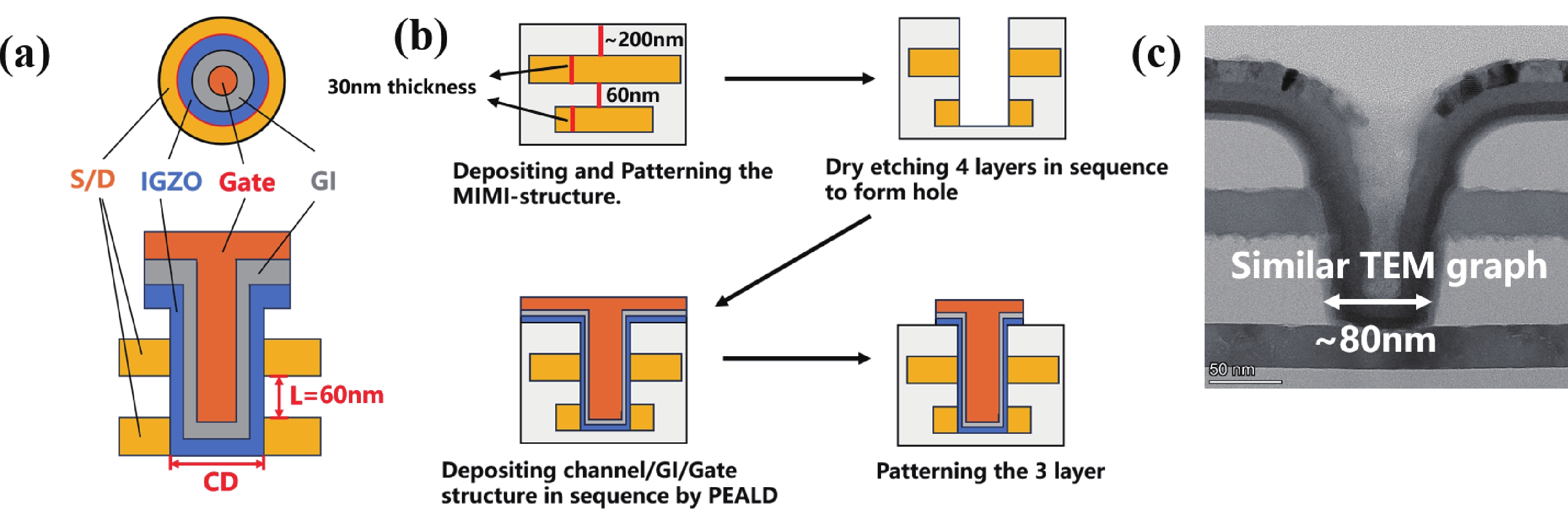
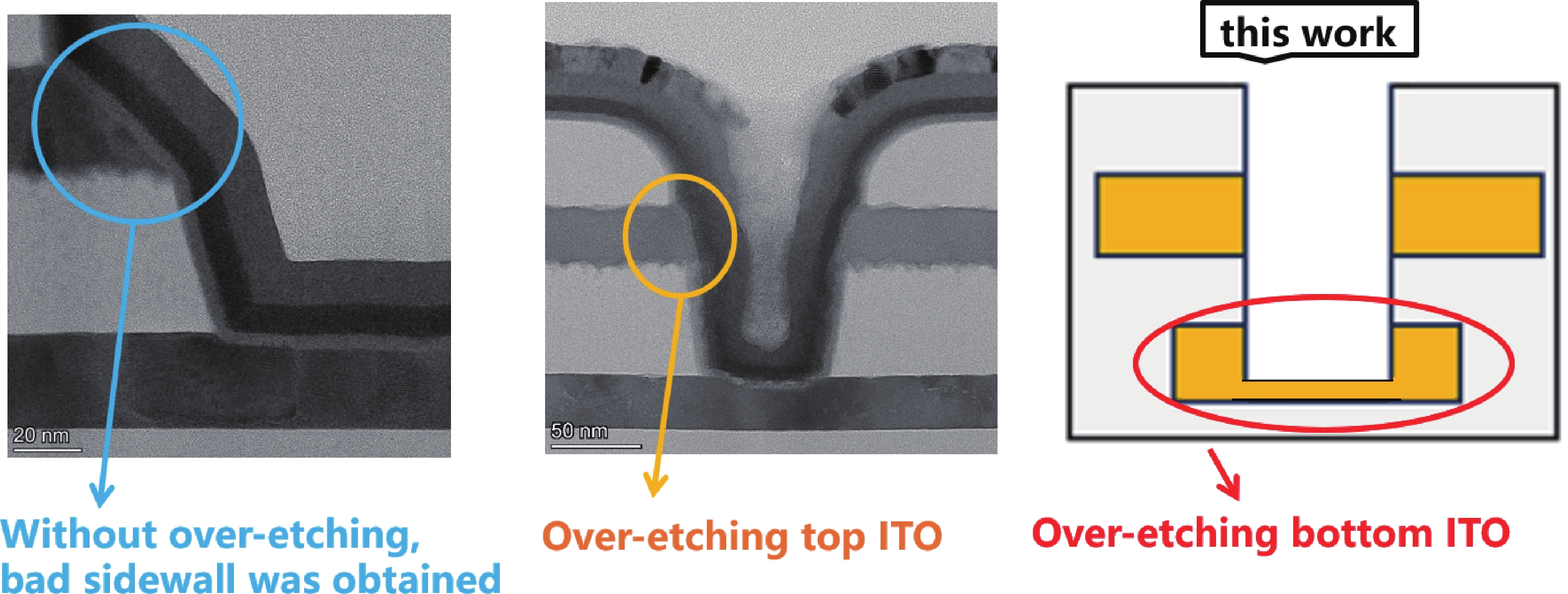
Fig. 1.
(Color online) (a) The channel-all-around IGZO-FET structure. (b) An illustration of the single FET layer fabrication process flow. (c) the similar cross-section TEM of the FET, which has CD that is ~80 nm.
ARTICLES
Yinzhi Tang1, Chuanke Chen2, Chunyu Zhang2, Congyan Lu2, Kaiping Zhang2, Jiebin Niu2, Shengjie Zhao2, Yu Liu2, Cheng Lu2, Cheng Huang2, Nianduan Lu2, Di Geng2 and Ling Li1, 2
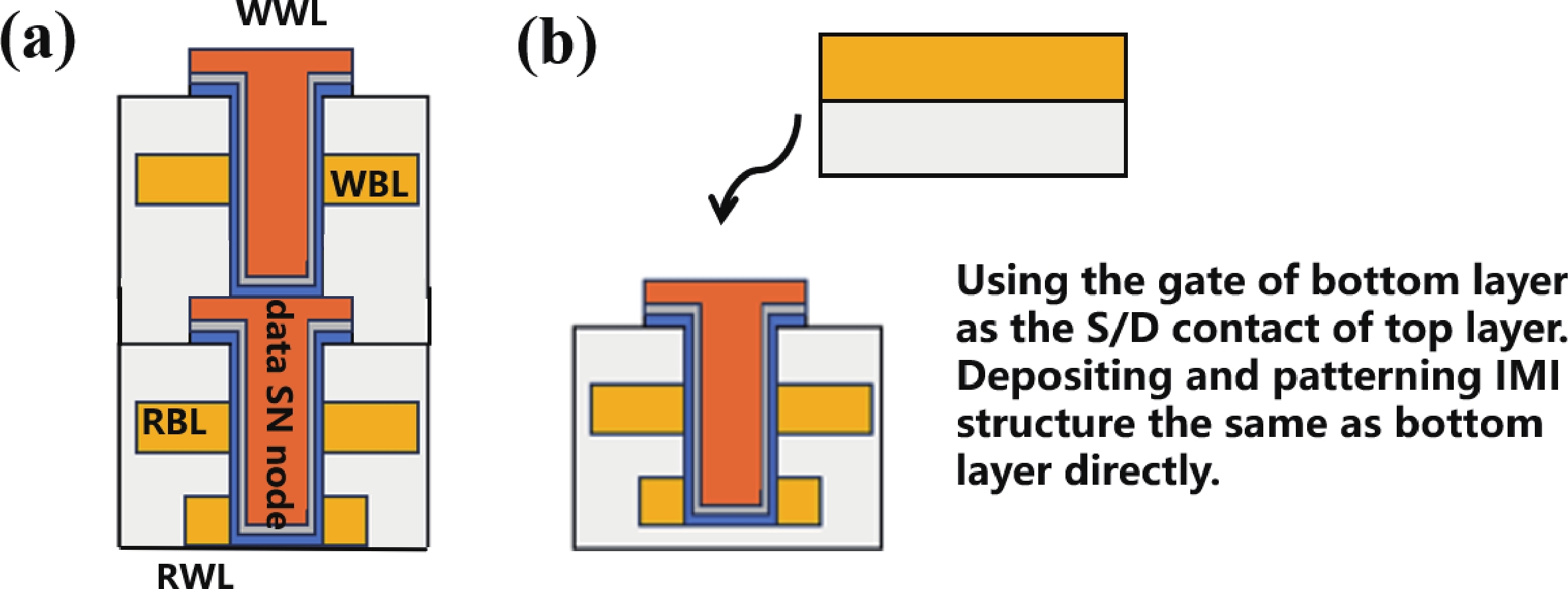
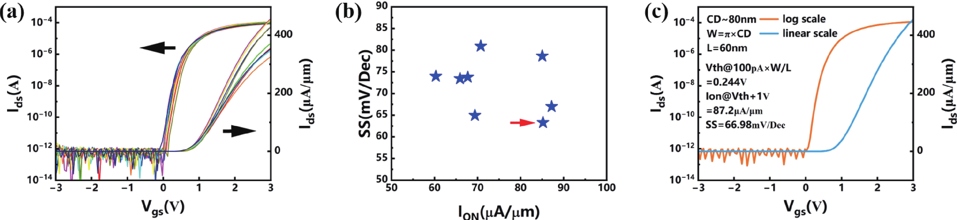
Abstract: This work fabricates a vertical channel-all-around indium-gallium-zinc-oxide field-effect transistor(CAA IGZO FET) through reasonable etching process and annealing optimization. The resulting device exhibits has a normalized on-current (ION) of 87.1 μA/μm, and a subthreshold swing (SS) of approximately 66.98 mV/Dec. These performance parameters are twice as good as similar work obtained in previous experiments, which is sufficient to meet the requirements for manufacturing 2T0C DRAM units. Moreover, with the double-layer stacking of this structure , the feasibility and scalability of manufacturing DRAM units with CAA IGZO FET is verified .
Keywords: amorphous indium-gallium-zinc-oxide, DRAM, channel-all-around
| [1] |
Zhang C Y, Chen C K, Tang Y Z, et al. Ultrahigh current vertical channel-all-around indium–gallium–zinc–oxide field-effect transistors using indium–tin–oxide electrode with sub-100 nm critical dimension. Phys Status Solidi RRL, 2025, 19(6): 2500027 doi: 10.1002/pssr.202500027
|
| [2] |
Chen C K, Gu C, Zhao Y, et al. Vertical channel-all-around (CAA) IGZO FET with recessed source/drain structure to improve contact characteristics. IEEE Electron Device Lett, 2025, 46(7): 1127 doi: 10.1109/LED.2025.3563839
|
| [3] |
Duan X L, Huang K L, Feng J X, et al. Novel vertical channel-all-around (CAA) In-Ga-Zn-O FET for 2T0C-DRAM with high density beyond 4F2 by monolithic stacking. IEEE Trans Electron Devices, 2022, 69(4): 2196 doi: 10.1109/TED.2022.3154693
|
| [4] |
Kim J Y, Kim H, Kim D, et al. Advancements of amorphous IGZO-based transistors: Materials, processing, and devices. ACS Appl Electron Mater, 2025, 7(11): 4703 doi: 10.1021/acsaelm.5c00605
|
| [5] |
Zhu Y, He Y L, Jiang S S, et al. Indium–gallium–zinc–oxide thin-film transistors: Materials, devices, and applications. J Semicond, 2021, 42(03): 031101 doi: 10.1088/1674-4926/42/3/031101
|
| [6] |
Fortunato E. , Barquinha P, Martins R. Oxide semiconductor thin-film transistors: A review of recent advances. Adv Mater, 2012, 24(22): 2945
|
| [7] |
Li Y B, Chen T P. Enhancement in performance and reliability of transparent IGZO thin-film transistors by ITO/Ti stacked source/drain contacts. ECS J Solid State Sci Technol, 2023, 12(9): 095003 doi: 10.1149/2162-8777/acf7f0
|
| [8] |
Zheng S, Wang C, Lv S, et al. Enhancement in performance and reliability of fully transparent a-IGZO top-gate thin-film transistors by a two-step annealing treatment. Nanomaterials, 2025, 15(6): 460 doi: 10.3390/nano15060460
|
| [9] |
Parthiban S, Kwon J Y. Role of dopants as a carrier suppressor and strong oxygen binder in amorphous indium-oxide-based field effect transistor. J Mater Res, 2014, 29(15): 1585 doi: 10.1557/jmr.2014.187
|
| [10] |
Lin Z Y, Kang L, Zhao J X, et al. The role of oxygen vacancy and hydrogen on the PBTI reliability of ALD IGZO transistors and process optimization. IEEE Trans Electron Devices, 2024, 71(5): 3002 doi: 10.1109/TED.2024.3374247
|
| [11] |
Hong J W, Cho H M, Jeong Y G, et al. Indium tin oxide etch characteristics using CxH2x+2(x=1, 2, 3)/Ar. Mater Sci Semicond Process, 2023, 160: 107395 doi: 10.1016/j.mssp.2023.107395
|
| [12] |
Yu W H, Lee J G, Joo Y H, et al. Etching characteristics and surface properties of fluorine-doped tin oxide thin films under CF4-based plasma treatment. Appl Phys A, 2022, 128(10): 942 doi: 10.1007/s00339-022-06082-y
|
| [13] |
Sun J B, Yu W, Zhang J, et al. In situ engineering of vertical indium gradients via sputtering kinetics for high-performance IGZO channel-all-around transistors. Nano Lett, 2026, 26(11): 3899 doi: 10.1021/acs.nanolett.6c00123
|
| [14] |
Liao F X, Zhu Z Y, Li Z H, et al. High-density three-dimensional integration of dynamic random-access memory using vertical dual-gate IGZO TFTs. Nat Commun, 2025, 16: 10932 doi: 10.1038/s41467-025-65925-3
|
| [15] |
Belmonte A, Oh H, Subhechha S, et al. Tailoring IGZO-TFT architecture for capacitorless DRAM, demonstrating > 103s retention, >1011 cycles endurance and Lg scalability down to 14 nm. 2021 IEEE International Electron Devices Meeting (IEDM). San Francisco, CA, USA. IEEE, 2022: 10.6.1
|
| [16] |
Lu W D, Zhu Z Y, Chen K F, et al. First demonstration of dual-gate IGZO 2T0C DRAM with novel read operation, one bit line in single cell, ION=1500 μA/μm@VDS=1 V and retention Time>300 s. 2022 International Electron Devices Meeting (IEDM), 2023: 26.4.1
|
| [17] |
Hu Q L, Li Q J, Zhu S W, et al. Optimized IGZO FETs for Capacitorless DRAM with Retention of 10 ks at RT and 7 ks at 85 °C at Zero Vhold with Sub-10 ns Speed and 3-bit Operation. 2022 International Electron Devices Meeting (IEDM), 2023: 26.6.1
|


Article views: 9 Times PDF downloads: 0 Times Cited by: 0 Times
Received: 20 March 2026 Revised: 13 May 2026 Online: Accepted Manuscript: 23 June 2026
| Citation: |
Yinzhi Tang, Chuanke Chen, Chunyu Zhang, Congyan Lu, Kaiping Zhang, Jiebin Niu, Shengjie Zhao, Yu Liu, Cheng Lu, Cheng Huang, Nianduan Lu, Di Geng, Ling Li. Fabrication of high-performance, sub-100 nm critical dimension vertical channel-all-around indium-gallium-zinc-oxide field-effect transistor and using for DRAM unit with optimized etching condition[J]. Journal of Semiconductors, 2026, In Press. doi: 10.1088/1674-4926/26030035
****
Y Z Tang, C K Chen, C Y Zhang, C Y Lu, K P Zhang, J B Niu, S J Zhao, Y Liu, C Lu, C Huang, N D Lu, D Geng, and L Li, Fabrication of high-performance, sub-100 nm critical dimension vertical channel-all-around indium-gallium-zinc-oxide field-effect transistor and using for DRAM unit with optimized etching condition[J]. J. Semicond., 2026, accepted doi: 10.1088/1674-4926/26030035

|
 YinZhi Tang got his B.E. from Tsinghua University at 2023. Now he is a ME student at University of Chinese Academy of Sciences under the supervision of Prof. Ling Li. His research focuses on amorphous metal oxide thin film transistor and DRAM
 Ling Li got his B.E. degreein in 2001 and ME degree in 2004 and PhD in Vienna University of Technology, Austria. He became senor researcher at IMEC in 2011 and research professor in Kyung Hee University ,korea in 2012. From then on he has been professor at lnstitution of University of Chinese Academy of Sciences, His research focuses on carriar transport , compact models and IC design
| [1] |
Zhang C Y, Chen C K, Tang Y Z, et al. Ultrahigh current vertical channel-all-around indium–gallium–zinc–oxide field-effect transistors using indium–tin–oxide electrode with sub-100 nm critical dimension. Phys Status Solidi RRL, 2025, 19(6): 2500027 doi: 10.1002/pssr.202500027
|
| [2] |
Chen C K, Gu C, Zhao Y, et al. Vertical channel-all-around (CAA) IGZO FET with recessed source/drain structure to improve contact characteristics. IEEE Electron Device Lett, 2025, 46(7): 1127 doi: 10.1109/LED.2025.3563839
|
| [3] |
Duan X L, Huang K L, Feng J X, et al. Novel vertical channel-all-around (CAA) In-Ga-Zn-O FET for 2T0C-DRAM with high density beyond 4F2 by monolithic stacking. IEEE Trans Electron Devices, 2022, 69(4): 2196 doi: 10.1109/TED.2022.3154693
|
| [4] |
Kim J Y, Kim H, Kim D, et al. Advancements of amorphous IGZO-based transistors: Materials, processing, and devices. ACS Appl Electron Mater, 2025, 7(11): 4703 doi: 10.1021/acsaelm.5c00605
|
| [5] |
Zhu Y, He Y L, Jiang S S, et al. Indium–gallium–zinc–oxide thin-film transistors: Materials, devices, and applications. J Semicond, 2021, 42(03): 031101 doi: 10.1088/1674-4926/42/3/031101
|
| [6] |
Fortunato E. , Barquinha P, Martins R. Oxide semiconductor thin-film transistors: A review of recent advances. Adv Mater, 2012, 24(22): 2945
|
| [7] |
Li Y B, Chen T P. Enhancement in performance and reliability of transparent IGZO thin-film transistors by ITO/Ti stacked source/drain contacts. ECS J Solid State Sci Technol, 2023, 12(9): 095003 doi: 10.1149/2162-8777/acf7f0
|
| [8] |
Zheng S, Wang C, Lv S, et al. Enhancement in performance and reliability of fully transparent a-IGZO top-gate thin-film transistors by a two-step annealing treatment. Nanomaterials, 2025, 15(6): 460 doi: 10.3390/nano15060460
|
| [9] |
Parthiban S, Kwon J Y. Role of dopants as a carrier suppressor and strong oxygen binder in amorphous indium-oxide-based field effect transistor. J Mater Res, 2014, 29(15): 1585 doi: 10.1557/jmr.2014.187
|
| [10] |
Lin Z Y, Kang L, Zhao J X, et al. The role of oxygen vacancy and hydrogen on the PBTI reliability of ALD IGZO transistors and process optimization. IEEE Trans Electron Devices, 2024, 71(5): 3002 doi: 10.1109/TED.2024.3374247
|
| [11] |
Hong J W, Cho H M, Jeong Y G, et al. Indium tin oxide etch characteristics using CxH2x+2(x=1, 2, 3)/Ar. Mater Sci Semicond Process, 2023, 160: 107395 doi: 10.1016/j.mssp.2023.107395
|
| [12] |
Yu W H, Lee J G, Joo Y H, et al. Etching characteristics and surface properties of fluorine-doped tin oxide thin films under CF4-based plasma treatment. Appl Phys A, 2022, 128(10): 942 doi: 10.1007/s00339-022-06082-y
|
| [13] |
Sun J B, Yu W, Zhang J, et al. In situ engineering of vertical indium gradients via sputtering kinetics for high-performance IGZO channel-all-around transistors. Nano Lett, 2026, 26(11): 3899 doi: 10.1021/acs.nanolett.6c00123
|
| [14] |
Liao F X, Zhu Z Y, Li Z H, et al. High-density three-dimensional integration of dynamic random-access memory using vertical dual-gate IGZO TFTs. Nat Commun, 2025, 16: 10932 doi: 10.1038/s41467-025-65925-3
|
| [15] |
Belmonte A, Oh H, Subhechha S, et al. Tailoring IGZO-TFT architecture for capacitorless DRAM, demonstrating > 103s retention, >1011 cycles endurance and Lg scalability down to 14 nm. 2021 IEEE International Electron Devices Meeting (IEDM). San Francisco, CA, USA. IEEE, 2022: 10.6.1
|
| [16] |
Lu W D, Zhu Z Y, Chen K F, et al. First demonstration of dual-gate IGZO 2T0C DRAM with novel read operation, one bit line in single cell, ION=1500 μA/μm@VDS=1 V and retention Time>300 s. 2022 International Electron Devices Meeting (IEDM), 2023: 26.4.1
|
| [17] |
Hu Q L, Li Q J, Zhu S W, et al. Optimized IGZO FETs for Capacitorless DRAM with Retention of 10 ks at RT and 7 ks at 85 °C at Zero Vhold with Sub-10 ns Speed and 3-bit Operation. 2022 International Electron Devices Meeting (IEDM), 2023: 26.6.1
|

 WeChat ID
Journal of Semiconductors © 2017 All Rights Reserved 京ICP备05085259号-2

 DownLoad:

