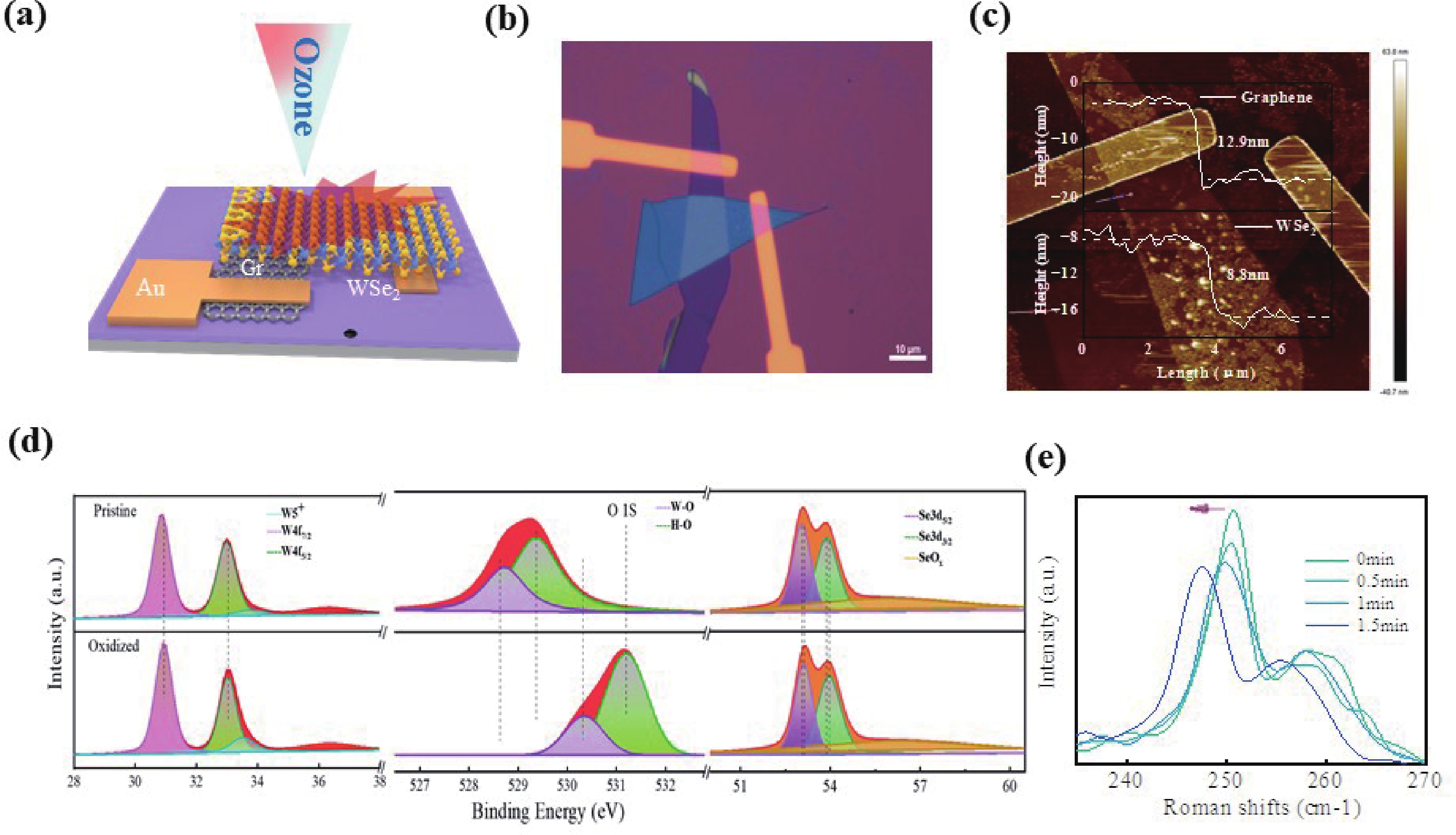
| [1] |
Shin Y S, Lee K, Kim Y R, et al. Mobility engineering in vertical field effect transistors based on van der Waals heterostructures. Adv Mater, 2018, 30(9): 1704435 doi: 10.1002/adma.201704435 |
| [2] |
Zhang Y, Yao Y Y, Sendeku M G, et al. Recent progress in CVD growth of 2D transition metal dichalcogenides and related heterostructures. Adv Mater, 2019, 31(41): 1901694 doi: 10.1002/adma.201901694 |
| [3] |
Pudasaini P R, Oyedele A, Zhang C, et al. High-performance multilayer WSe 2 field-effect transistors with carrier type control. Nano Res, 2018, 11(2): 722 doi: 10.1007/s12274-017-1681-5 |
| [4] |
Mak K F, Xiao D, Shan J. Light–valley interactions in 2D semiconductors. Nat Photonics, 2018, 12(8): 451 doi: 10.1038/s41566-018-0204-6 |
| [5] |
Dai M J, Zhang X R, Wang Q J. 2D materials for photothermoelectric detectors: Mechanisms, materials, and devices. Adv Funct Mater, 2024, 34(21): 2312872 doi: 10.1002/adfm.202312872 |
| [6] |
Chen W Y, Li L, Huang T, et al. Extending Schottky–Mott rule to van der Waals heterostructures of 2D Janus materials: Influence of intrinsic dipoles. Appl Phys Lett, 2023, 123(17): 171601 doi: 10.1063/5.0174594 |
| [7] |
Nishio K, Shirasawa T, Shimizu K, et al. Tuning the Schottky barrier height at the interfaces of metals and mixed conductors. ACS Appl Mater Interfaces, 2021, 13(13): 15746 doi: 10.1021/acsami.0c18656 |
| [8] |
Boehm A, Fonseca J J, Thürmer K, et al. Engineering of nanoscale heterogeneous transition metal dichalcogenide–Au interfaces. Nano Lett, 2023, 23(7): 2792 doi: 10.1021/acs.nanolett.3c00080 |
| [9] |
Padilha J E, Fazzio A, da Silva A J R. Van der Waals heterostructure of phosphorene and graphene: Tuning the Schottky barrier and doping by electrostatic gating. Phys Rev Lett, 2015, 114(6): 066803 doi: 10.1103/PhysRevLett.114.066803 |
| [10] |
Zhao Z J, Kang J Z, Rakheja S, et al. Control-gate-free reconfigurable transistor based on 2D MoTe 2 with asymmetric gating. Appl Phys Lett, 2024, 124(7): 073506 doi: 10.1063/5.0177275 |
| [11] |
Guo Y G, Wang F Q, Wang Q. An all-carbon vdW heterojunction composed of penta-graphene and graphene: Tuning the Schottky barrier by electrostatic gating or nitrogen doping. Appl Phys Lett, 2017, 111(7): 073503 doi: 10.1063/1.4986604 |
| [12] |
Xu D, Zhang S N, Chen J S, et al. Design of the synergistic rectifying interfaces in Mott–Schottky catalysts. Chem Rev, 2023, 123(1): 1 doi: 10.1021/acs.chemrev.2c00426 |
| [13] |
Chen Y K, Wang X Q, Cui W G, et al. Multiple Schottky contacts motivated via defects to tune the response ability of electromagnetic waves. Adv Funct Mater, 2025, 35(11): 2417215 doi: 10.1002/adfm.202417215 |
| [14] |
Zhang Z, Qiu Z J, Liu R, et al. Schottky-barrier height tuning by means of ion implantation into preformed silicide films followed by drive-In anneal. IEEE Electron Device Lett, 2007, 28(7): 565 doi: 10.1109/LED.2007.900295 |
| [15] |
Aswini K, Kunapalli C K, Munirathnam K, et al. Tuning barrier height and enhancing electrical properties of MOS heterojunctions using Fe 2O 3 doped MoO 3 nanocomposite interlayer on Ni/Cr/n-GaN for optoelectronic devices. Phys B Condens Matter, 2025, 714: 417422 doi: 10.1016/j.physb.2025.417422 |
| [16] |
Kaur D, Dahiya R, Shivani, et al. Interface-induced origin of Schottky-to-Ohmic-to-Schottky conversion in non-conventional contact to β-Ga 2O 3. Appl Phys Lett, 2024, 124(2): 021601 doi: 10.1063/5.0187009 |
| [17] |
Zhang G B, Fan X M, Wang Z J, et al. Self-rectifying memristors for beyond-CMOS computing: Mechanisms, materials, and integration prospects. Nano Micro Lett, 2026, 18(1): 188 doi: 10.1007/s40820-025-02035-1 |
| [18] |
Fenouillet-Beranger C, Brunet L, Batude P, et al. A review of low temperature process modules leading up to the first (≤500 °C) planar FDSOI CMOS devices for 3-D sequential integration. IEEE Trans Electron Devices, 2021, 68(7): 3142 doi: 10.1109/TED.2021.3084916 |
| [19] |
Arora R, Barr A R, Larson D T, et al. Engineering interfacial charge transfer through modulation doping for 2D electronics. Phys Rev Materials, 2025, 9(2): L021601 doi: 10.1103/PhysRevMaterials.9.L021601 |
| [20] |
Shinde P A, Mahamiya V, Safarkhani M, et al. Unveiling the nanoarchitectonics of interfacial electronic coupling in atomically thin 2D WO 3/WSe 2 heterostructure for sodium-ion storage in aqueous system. Adv Funct Mater, 2024, 34(41): 2406333 doi: 10.1002/adfm.202406333 |
| [21] |
Martín-Sánchez J, Mariscal A, De Luca M, et al. Effects of dielectric stoichiometry on the photoluminescence properties of encapsulated WSe 2 monolayers. Nano Res, 2018, 11(3): 1399 doi: 10.1007/s12274-017-1755-4 |
| [22] |
Lu J P, Carvalho A, Chan X K, et al. Atomic healing of defects in transition metal dichalcogenides. Nano Lett, 2015, 15(5): 3524 doi: 10.1021/acs.nanolett.5b00952 |
| [23] |
Jiang Y R, Xing W Q, Li H Z, et al. Controllable carrier concentration of two-dimensional TMDs by forming transition-metal suboxide layer for photoelectric devices. Appl Phys Lett, 2022, 121(2): 022101 doi: 10.1063/5.0097392 |


 Yiwen Bian Bian Yiwen, an undergraduate student of the 2024 batch, is currently studying in the School of International Education at Henan Normal University, majoring in Electrical Engineering and Automation.
 Caixia Guo was born in Yucheng, Henan, China, in 1979. She received the M.S. degree from Nanjing University of Science and Technology, Nanjing, China, in 2005 and the Ph.D. degree from Henan Normal University, Xinxiang, China, in 2018. She is currently an Associate Professor with Henan Normal University, Xinxiang. Her current research interests include 2D semiconductor materials and devices.
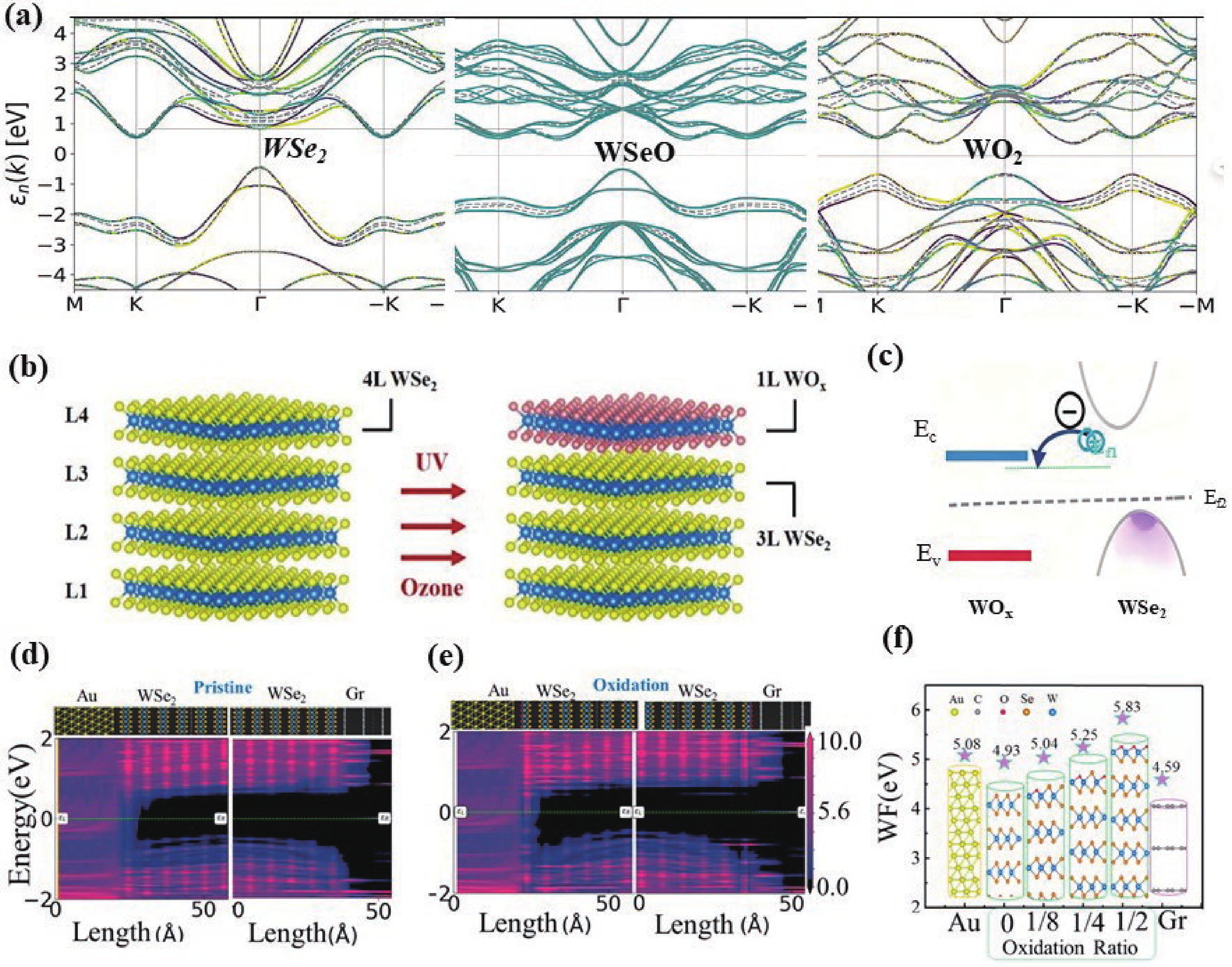
 DownLoad: