


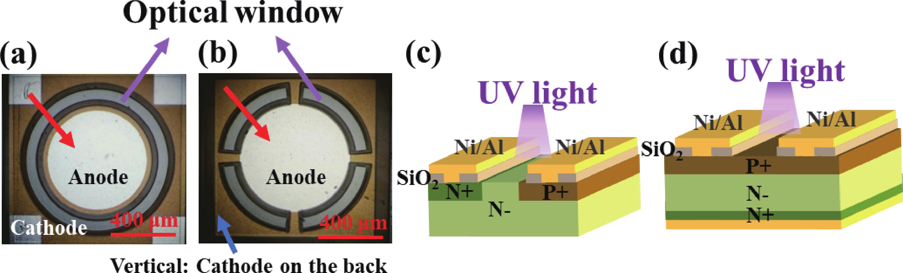
Fig. 1.
(Color online) The optical micrograph of (a) the lateral and (b) vertical PIN diodes. The cross-sectional views in (c) and (d) are taken along the red arrows indicated in (a) and (b), respectively.
ARTICLES
Xuan Tang1, 2, Zhanwei Shen1, 2, , Guoliang Zhang3, Jinyi Xu1, 2, Hangshuo Shi1, 2, Zhihai Yang3, Xi Wang4, Yanan Guo1, 2, Chao Li5, , Shizhong Yue1, 2, Feng Zhang3, and Zhijie Wang1, 2,
Corresponding author: Zhanwei Shen, zwshen@semi.ac.cn; Chao Li, lichao@bise.hrl.ac.cn; Feng Zhang, fzhang@xmu.edu.cn; Zhijie Wang, wangzj@semi.ac.cn
Abstract: We demonstrate a significant light-triggered current enhancement in SiC bipolar PIN diodes through ultraviolet (UV) light injection, achieving a 2.74× current gain at 3.5 V under 365 nm illumination. By integrating an optical window for targeted photon injection into the intrinsic region, UV-generated electron-hole pairs enhance conductivity modulation and lower the forward voltage drop. Crucially, we reveal a pronounced structural dependence: vertical devices outperform lateral counterparts due to more effective utilization of photogenerated carriers. This advantage stems from shorter carrier transport path of the vertical architecture and reduced surface recombination losses, whereas lateral devices suffer from enhanced carrier recombination due to surface-parallel carrier drift. This study establishes UV illumination as a scalable and non-invasive strategy for dynamic performance tuning of SiC bipolar devices, bypassing complex lifetime-enhancement processes while enabling adaptive conduction for smart power systems.
Keywords: SiC, bipolar diodes, high current, UV light, conductivity modulation, vertical device
| [1] |
Singh R, Cooper J A, Melloch M R, et al. SiC power Schottky and PiN diodes. IEEE Trans Electron Devices, 2002, 49(4): 665 doi: 10.1109/16.992877
|
| [2] |
Kato M, Watanabe O, Mii T, et al. Suppression of stacking-fault expansion in 4H-SiC PiN diodes using proton implantation to solve bipolar degradation. Sci Rep, 2022, 12: 18790 doi: 10.1038/s41598-022-23691-y
|
| [3] |
Cheng L, Palmour J W, Agarwal A K, et al. Strategic overview of high-voltage SiC power device development aiming at global energy savings. Mater Sci Forum, 2014, 778/779/780: 1089
|
| [4] |
Almpanis I, Antoniou M, Evans P, et al. Silicon carbide n-IGBTs: Structure optimization for ruggedness enhancement. IEEE Trans Ind Appl, 2024, 60(3): 4251 doi: 10.1109/TIA.2024.3354870
|
| [5] |
Watanabe N, Okino H, Shimizu H, et al. Power loss reduction of N-channel 10-kV SiC IGBTs with box cell layout. IEEE Trans Electron Devices, 2023, 70(7): 3768 doi: 10.1109/TED.2023.3279799
|
| [6] |
Yu Q S, Huang J, Shen Z G, et al. 16kV 4H-SiC reverse-conducting IGBT with a collector-side injection-enhanced structure for low reverse-conducting voltage. IEEE Electron Device Lett, 2024, 45(6): 1064 doi: 10.1109/LED.2024.3386769
|
| [7] |
Chowdhury S, Chow T P. Performance tradeoffs for ultra-high voltage (15 kV to 25 kV) 4H-SiC n-channel and p-channel IGBTs. 2016 28th International Symposium on Power Semiconductor Devices and ICs (ISPSD, 2016: 75 .
|
| [8] |
Ryu S H, Capell C, Cheng L, et al. High performance, ultra high voltage 4H-SiC IGBTs. 2012 IEEE Energy Conversion Congress and Exposition (ECCE). Raleigh: IEEE, 2012: 3603
|
| [9] |
Singh R, Irvine K G, Capell D C, et al. Large area, ultra-high voltage 4H-SiC p-i-n rectifiers. IEEE Trans Electron Devices, 2002, 49(12): 2308 doi: 10.1109/TED.2002.805576
|
| [10] |
Wen Z X, Zhang F, Shen Z W, et al. A novel silicon carbide accumulation channel injection enhanced gate transistor with buried barrier under shielding region. IEEE Electron Device Lett, 2017, 38(7): 941 doi: 10.1109/LED.2017.2709322
|
| [11] |
Khera F A, Xie J, Wheeler P. Advanced SSPC based on SiC-MOSFET for aircraft applications. 2024 IEEE Energy Conversion Congress and Exposition (ECCE). Phoenix: IEEE, 2025: 2318
|
| [12] |
Shang H, Liang L, Han L B, et al. Design key points and multi-field simulations for half bridge module of converter valve based on SiC IGBT. 2020 IEEE 4th Conference on Energy Internet and Energy System Integration (EI2), 2020: 1031
|
| [13] |
Danno K, Nakamura D, Kimoto T. Investigation of carrier lifetime in 4H-SiC epilayers and lifetime control by electron irradiation. Appl Phys Lett, 2007, 90(20): 202109 doi: 10.1063/1.2740580
|
| [14] |
Storasta L, Tsuchida H. Reduction of traps and improvement of carrier lifetime in 4H-SiC epilayers by ion implantation. Appl Phys Lett, 2007, 90(6): 062116 doi: 10.1063/1.2472530
|
| [15] |
Nishio J, Kushibe M, Asamizu H, et al. Reduction of background carrier concentration and lifetime improvement for 4H-SiC C-face epitaxial growth. Jpn J Appl Phys, 2017, 56(8): 081302 doi: 10.7567/JJAP.56.081302
|
| [16] |
Hiyoshi T, Kimoto T. Elimination of the major deep levels in n- and p-type 4H-SiC by two-step thermal treatment. Appl Phys Express, 2009, 2(9): 091101 doi: 10.1143/APEX.2.091101
|
| [17] |
Ayedh H M, Nipoti R, Hallén A, et al. Elimination of carbon vacancies in 4H-SiC employing thermodynamic equilibrium conditions at moderate temperatures. Appl Phys Lett, 2015, 107(25): 252102 doi: 10.1063/1.4938242
|
| [18] |
Negoro Y, Katsumoto K, Kimoto T, et al. Electronic behaviors of high-dose phosphorus-ion implanted 4H-SiC (0001). J Appl Phys, 2004, 96(1): 224 doi: 10.1063/1.1756213
|
| [19] |
Kawahara K, Jun S D, Kimoto T. Analytical model for reduction of deep levels in SiC by thermal oxidation. J Appl Phys, 2012, 111(5): 053710 doi: 10.1063/1.3692766
|
| [20] |
Kaji N, Niwa H, Jun S D, et al. Ultrahigh-voltage SiC p-i-n diodes with improved forward characteristics. IEEE Trans Electron Devices, 2015, 62(2): 374 doi: 10.1109/TED.2014.2352279
|
| [21] |
Wang J, Ardelean J, Bai Y S, et al. Optical generation of high carrier densities in 2D semiconductor heterobilayers. Sci Adv, 2019, 5(9): eaax0145 doi: 10.1126/sciadv.aax0145
|
| [22] |
Mics Z, D’Angio A, Jensen S A, et al. Density-dependent electron scattering in photoexcited GaAs in strongly diffusive regime. Appl Phys Lett, 2013, 102(23): 231120 doi: 10.1063/1.4810756
|
| [23] |
Fan M H, Cen W F, Cai X M, et al. The defects regulating for the electronic structure and optical properties of 4H-SiC with (0001) surface. Appl Surf Sci, 2018, 427: 851 doi: 10.1016/j.apsusc.2017.08.173
|
| [24] |
Song W D, Chen J X, Li Z L, et al. Self-powered MXene/GaN van der Waals heterojunction ultraviolet photodiodes with superhigh efficiency and stable current outputs. Adv Mater, 2021, 33(27): 2101059 doi: 10.1002/adma.202101059
|
| [25] |
Wang X, Xu B, Pu H B, et al. Monolithic integration of 1.2kV optically-controlled SiC npn transistor and antiparallel diode. IEEE Electron Device Lett, 2022, 43(9): 1531 doi: 10.1109/LED.2022.3192457
|
| [26] |
Zhao F, Islam M M. Optically activated SiC power transistors for pulsed-power application. IEEE Electron Device Lett, 2010, 31(10): 1146 doi: 10.1109/LED.2010.2058840
|
| [27] |
Hsia J H, Perozek J A, Palacios T. First demonstration of optically-controlled vertical GaN finFET for power applications. IEEE Electron Device Lett, 2024, 45(5): 774 doi: 10.1109/LED.2024.3375856
|
| [28] |
Koehler A D, Anderson T J, Khachatrian A, et al. High voltage GaN lateral photoconductive semiconductor switches. ECS J Solid State Sci Technol, 2017, 6(11): S3099 doi: 10.1149/2.0231711jss
|
| [29] |
Chen Y F, Lu H, Chen D J, et al. High-voltage photoconductive semiconductor switches fabricated on semi-insulating HVPE GaN: Fe template. Phys Status Solidi C, 2016, 13(5/6): 374
|
| [30] |
Chang Y F, Liao C L, Zheng B S, et al. Using two-step mesa to prevent the effects of sidewall defects on the GaN p-i-n diodes. IEEE J Quantum Electron, 2015, 51(10): 8300106 doi: 10.1109/jqe.2015.2479465
|
| [31] |
Sozzi G, Puzzanghera M, Chiorboli G, et al. OCVD lifetime measurements on 4H-SiC bipolar planar diodes: Dependences on carrier injection and diode area. IEEE Trans Electron Devices, 2017, 64(6): 2572 doi: 10.1109/TED.2017.2691280
|
| [32] |
Zheng Z, Jiang S N, Sun Q, et al. Effects of illumination on space-charge-limited current in 4H-SiC photoconductive semiconductor switches. IEEE Trans Electron Devices, 2025, 72(8): 4290 doi: 10.1109/TED.2025.3577153
|
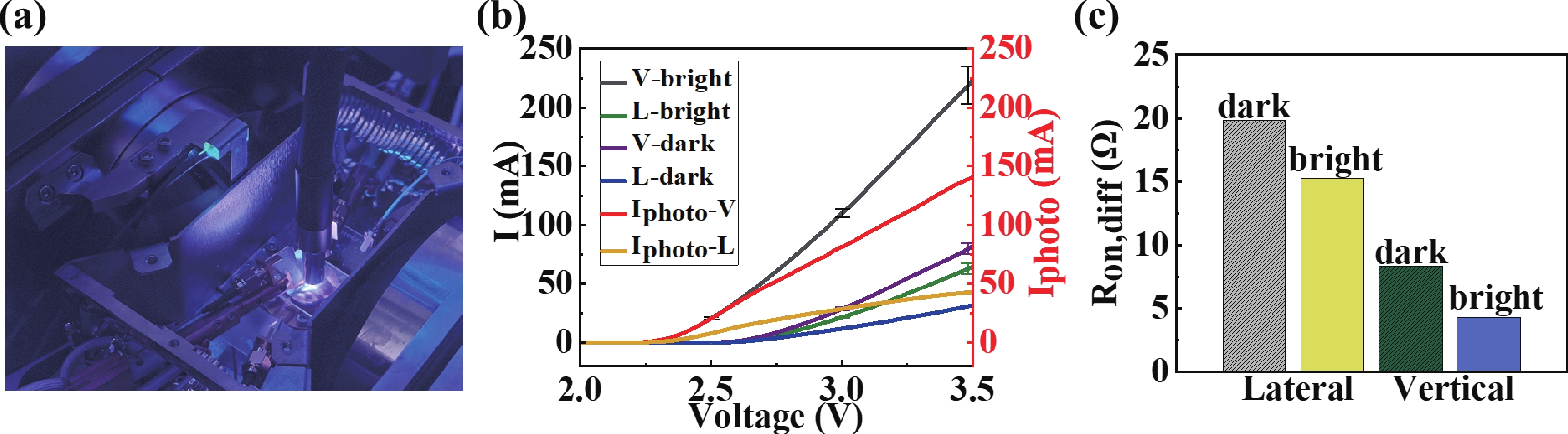
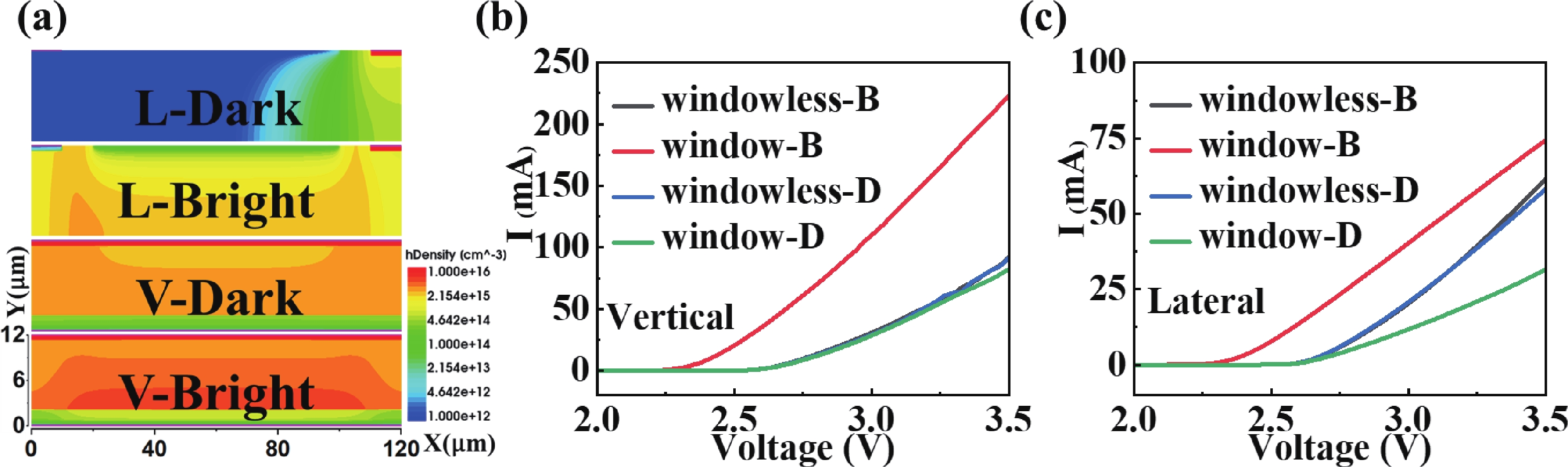
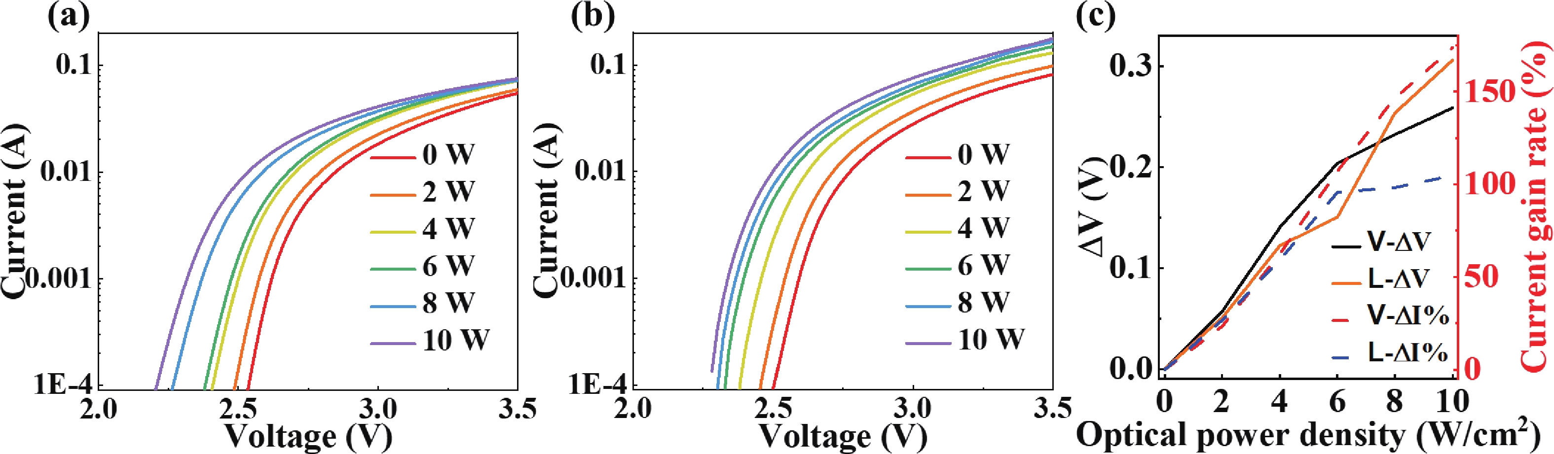
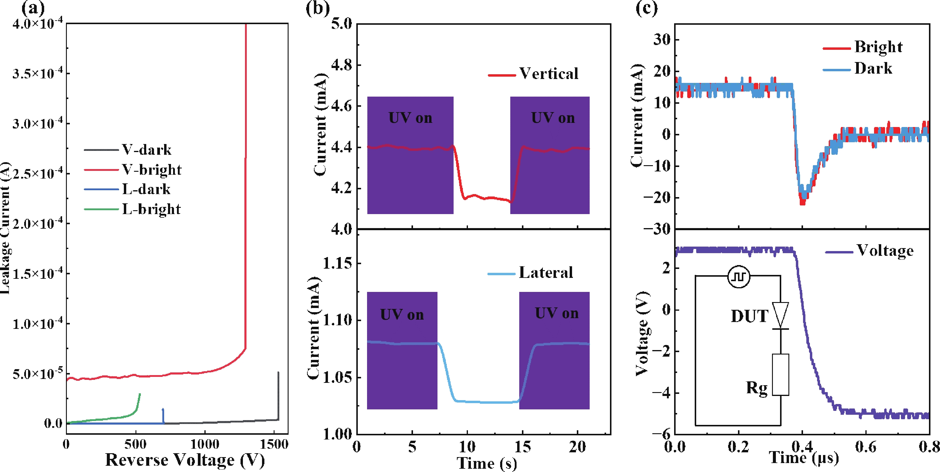
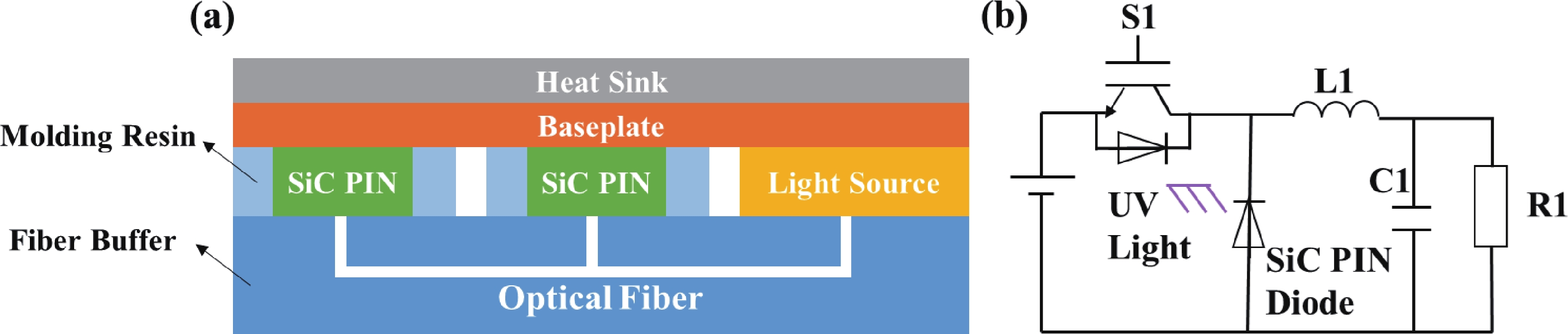
Table 1. Comparison with other wide-bandgap, optically controlled devices.
| Ref | BV (kV) | Persistent Photo-current | Optical Source | Device Type |
| [20] | 26.9(268 μm) | No | - | Lifetime-enhanced SiC pin diode (21.6 μs) |
| [24] | - | Yes | 355 nm laser | Ti3C2Tx/GaN photodiode |
| [25] | 1.2 | Yes | 365 nm LED | SiC optical transistor |
| [26] | - | No | 337 nm laser | SiC power transistor |
| [27] | - | Yes | 365 nm LED | Vertical GaN finFET |
| [28] | 4 | Yes | 293 nm laser | Lateral GaN PCSS |
| [29] | 1.1 | No | 266 nm laser | Vertical GaN PCSS |
| this work | 1.53 | Yes | 365 nm LED | SiC optical pin diode |
 DownLoad: CSV
| [1] |
Singh R, Cooper J A, Melloch M R, et al. SiC power Schottky and PiN diodes. IEEE Trans Electron Devices, 2002, 49(4): 665 doi: 10.1109/16.992877
|
| [2] |
Kato M, Watanabe O, Mii T, et al. Suppression of stacking-fault expansion in 4H-SiC PiN diodes using proton implantation to solve bipolar degradation. Sci Rep, 2022, 12: 18790 doi: 10.1038/s41598-022-23691-y
|
| [3] |
Cheng L, Palmour J W, Agarwal A K, et al. Strategic overview of high-voltage SiC power device development aiming at global energy savings. Mater Sci Forum, 2014, 778/779/780: 1089
|
| [4] |
Almpanis I, Antoniou M, Evans P, et al. Silicon carbide n-IGBTs: Structure optimization for ruggedness enhancement. IEEE Trans Ind Appl, 2024, 60(3): 4251 doi: 10.1109/TIA.2024.3354870
|
| [5] |
Watanabe N, Okino H, Shimizu H, et al. Power loss reduction of N-channel 10-kV SiC IGBTs with box cell layout. IEEE Trans Electron Devices, 2023, 70(7): 3768 doi: 10.1109/TED.2023.3279799
|
| [6] |
Yu Q S, Huang J, Shen Z G, et al. 16kV 4H-SiC reverse-conducting IGBT with a collector-side injection-enhanced structure for low reverse-conducting voltage. IEEE Electron Device Lett, 2024, 45(6): 1064 doi: 10.1109/LED.2024.3386769
|
| [7] |
Chowdhury S, Chow T P. Performance tradeoffs for ultra-high voltage (15 kV to 25 kV) 4H-SiC n-channel and p-channel IGBTs. 2016 28th International Symposium on Power Semiconductor Devices and ICs (ISPSD, 2016: 75 .
|
| [8] |
Ryu S H, Capell C, Cheng L, et al. High performance, ultra high voltage 4H-SiC IGBTs. 2012 IEEE Energy Conversion Congress and Exposition (ECCE). Raleigh: IEEE, 2012: 3603
|
| [9] |
Singh R, Irvine K G, Capell D C, et al. Large area, ultra-high voltage 4H-SiC p-i-n rectifiers. IEEE Trans Electron Devices, 2002, 49(12): 2308 doi: 10.1109/TED.2002.805576
|
| [10] |
Wen Z X, Zhang F, Shen Z W, et al. A novel silicon carbide accumulation channel injection enhanced gate transistor with buried barrier under shielding region. IEEE Electron Device Lett, 2017, 38(7): 941 doi: 10.1109/LED.2017.2709322
|
| [11] |
Khera F A, Xie J, Wheeler P. Advanced SSPC based on SiC-MOSFET for aircraft applications. 2024 IEEE Energy Conversion Congress and Exposition (ECCE). Phoenix: IEEE, 2025: 2318
|
| [12] |
Shang H, Liang L, Han L B, et al. Design key points and multi-field simulations for half bridge module of converter valve based on SiC IGBT. 2020 IEEE 4th Conference on Energy Internet and Energy System Integration (EI2), 2020: 1031
|
| [13] |
Danno K, Nakamura D, Kimoto T. Investigation of carrier lifetime in 4H-SiC epilayers and lifetime control by electron irradiation. Appl Phys Lett, 2007, 90(20): 202109 doi: 10.1063/1.2740580
|
| [14] |
Storasta L, Tsuchida H. Reduction of traps and improvement of carrier lifetime in 4H-SiC epilayers by ion implantation. Appl Phys Lett, 2007, 90(6): 062116 doi: 10.1063/1.2472530
|
| [15] |
Nishio J, Kushibe M, Asamizu H, et al. Reduction of background carrier concentration and lifetime improvement for 4H-SiC C-face epitaxial growth. Jpn J Appl Phys, 2017, 56(8): 081302 doi: 10.7567/JJAP.56.081302
|
| [16] |
Hiyoshi T, Kimoto T. Elimination of the major deep levels in n- and p-type 4H-SiC by two-step thermal treatment. Appl Phys Express, 2009, 2(9): 091101 doi: 10.1143/APEX.2.091101
|
| [17] |
Ayedh H M, Nipoti R, Hallén A, et al. Elimination of carbon vacancies in 4H-SiC employing thermodynamic equilibrium conditions at moderate temperatures. Appl Phys Lett, 2015, 107(25): 252102 doi: 10.1063/1.4938242
|
| [18] |
Negoro Y, Katsumoto K, Kimoto T, et al. Electronic behaviors of high-dose phosphorus-ion implanted 4H-SiC (0001). J Appl Phys, 2004, 96(1): 224 doi: 10.1063/1.1756213
|
| [19] |
Kawahara K, Jun S D, Kimoto T. Analytical model for reduction of deep levels in SiC by thermal oxidation. J Appl Phys, 2012, 111(5): 053710 doi: 10.1063/1.3692766
|
| [20] |
Kaji N, Niwa H, Jun S D, et al. Ultrahigh-voltage SiC p-i-n diodes with improved forward characteristics. IEEE Trans Electron Devices, 2015, 62(2): 374 doi: 10.1109/TED.2014.2352279
|
| [21] |
Wang J, Ardelean J, Bai Y S, et al. Optical generation of high carrier densities in 2D semiconductor heterobilayers. Sci Adv, 2019, 5(9): eaax0145 doi: 10.1126/sciadv.aax0145
|
| [22] |
Mics Z, D’Angio A, Jensen S A, et al. Density-dependent electron scattering in photoexcited GaAs in strongly diffusive regime. Appl Phys Lett, 2013, 102(23): 231120 doi: 10.1063/1.4810756
|
| [23] |
Fan M H, Cen W F, Cai X M, et al. The defects regulating for the electronic structure and optical properties of 4H-SiC with (0001) surface. Appl Surf Sci, 2018, 427: 851 doi: 10.1016/j.apsusc.2017.08.173
|
| [24] |
Song W D, Chen J X, Li Z L, et al. Self-powered MXene/GaN van der Waals heterojunction ultraviolet photodiodes with superhigh efficiency and stable current outputs. Adv Mater, 2021, 33(27): 2101059 doi: 10.1002/adma.202101059
|
| [25] |
Wang X, Xu B, Pu H B, et al. Monolithic integration of 1.2kV optically-controlled SiC npn transistor and antiparallel diode. IEEE Electron Device Lett, 2022, 43(9): 1531 doi: 10.1109/LED.2022.3192457
|
| [26] |
Zhao F, Islam M M. Optically activated SiC power transistors for pulsed-power application. IEEE Electron Device Lett, 2010, 31(10): 1146 doi: 10.1109/LED.2010.2058840
|
| [27] |
Hsia J H, Perozek J A, Palacios T. First demonstration of optically-controlled vertical GaN finFET for power applications. IEEE Electron Device Lett, 2024, 45(5): 774 doi: 10.1109/LED.2024.3375856
|
| [28] |
Koehler A D, Anderson T J, Khachatrian A, et al. High voltage GaN lateral photoconductive semiconductor switches. ECS J Solid State Sci Technol, 2017, 6(11): S3099 doi: 10.1149/2.0231711jss
|
| [29] |
Chen Y F, Lu H, Chen D J, et al. High-voltage photoconductive semiconductor switches fabricated on semi-insulating HVPE GaN: Fe template. Phys Status Solidi C, 2016, 13(5/6): 374
|
| [30] |
Chang Y F, Liao C L, Zheng B S, et al. Using two-step mesa to prevent the effects of sidewall defects on the GaN p-i-n diodes. IEEE J Quantum Electron, 2015, 51(10): 8300106 doi: 10.1109/jqe.2015.2479465
|
| [31] |
Sozzi G, Puzzanghera M, Chiorboli G, et al. OCVD lifetime measurements on 4H-SiC bipolar planar diodes: Dependences on carrier injection and diode area. IEEE Trans Electron Devices, 2017, 64(6): 2572 doi: 10.1109/TED.2017.2691280
|
| [32] |
Zheng Z, Jiang S N, Sun Q, et al. Effects of illumination on space-charge-limited current in 4H-SiC photoconductive semiconductor switches. IEEE Trans Electron Devices, 2025, 72(8): 4290 doi: 10.1109/TED.2025.3577153
|





Article views: 2 Times PDF downloads: 1 Times Cited by: 0 Times
Received: 29 March 2026 Revised: 30 May 2026 Online: Accepted Manuscript: 14 July 2026
| Citation: |
Xuan Tang, Zhanwei Shen, Guoliang Zhang, Jinyi Xu, Hangshuo Shi, Zhihai Yang, Xi Wang, Yanan Guo, Chao Li, Shizhong Yue, Feng Zhang, Zhijie Wang. High current handling capability in 4H-SiC bipolar diodes via ultraviolet illumination[J]. Journal of Semiconductors, 2026, In Press. doi: 10.1088/1674-4926/26030047
****
X Tang, Z W Shen, G L Zhang, J Y Xu, H S Shi, Z H Yang, X Wang, Y N Guo, C Li, S Z Yue, F Zhang, and Z J Wang, High current handling capability in 4H-SiC bipolar diodes via ultraviolet illumination[J]. J. Semicond., 2026, accepted doi: 10.1088/1674-4926/26030047

|
 Xuan Tang is a PhD candidate at the Institute of Semiconductors, Chinese Academy of Sciences. He earned his B.S. degree from the University of Chinese Academy of Sciences. His current research interest focuses on silicon carbide (SiC) power devices
 Zhanwei Shen is an associate professor in the Institute of Semiconductors, Chinese Academy of Sciences, China. He earned his B.S. degree from Xidian University and Ph.D. degree from the University of Chinese Academy of Sciences. His current research interests focus on silicon carbide (SiC) power devices, high-temperature sensors, and related gate dielectric and interface engineering technologies
 Chao Li is currently a scientist of Beijing Huairou Laboratory. He received his B.S. degree from North China Electric Power University in 2018, and his Ph.D. degree from the Institute of Semiconductors, Chinese Academy of Sciences, in 2023. His current research interests focus on power semiconductor device design and packaging technology
 Feng Zhang is a professor in the School of Physics and Astronomy, Xiamen University. He earned his Ph.D. degree from Xiamen University. His current research interests focus on wide-bandgap semiconductors, including ultraviolet optoelectronic devices of wide-bandgap semiconductors, research on deep-level defects and minority carrier lifetime in wide-bandgap semiconductors
 Zhijie Wang is a professor in the Institute of Semiconductors, Chinese Academy of Sciences, China. He earned his B.S. degree from Zhejiang University and Ph.D. degree in Engineering from the Institute of Semiconductors, Chinese Academy of Sciences. His current research interests focus on semiconductor micro-nano optics, semiconductor power electronic devices
| [1] |
Singh R, Cooper J A, Melloch M R, et al. SiC power Schottky and PiN diodes. IEEE Trans Electron Devices, 2002, 49(4): 665 doi: 10.1109/16.992877
|
| [2] |
Kato M, Watanabe O, Mii T, et al. Suppression of stacking-fault expansion in 4H-SiC PiN diodes using proton implantation to solve bipolar degradation. Sci Rep, 2022, 12: 18790 doi: 10.1038/s41598-022-23691-y
|
| [3] |
Cheng L, Palmour J W, Agarwal A K, et al. Strategic overview of high-voltage SiC power device development aiming at global energy savings. Mater Sci Forum, 2014, 778/779/780: 1089
|
| [4] |
Almpanis I, Antoniou M, Evans P, et al. Silicon carbide n-IGBTs: Structure optimization for ruggedness enhancement. IEEE Trans Ind Appl, 2024, 60(3): 4251 doi: 10.1109/TIA.2024.3354870
|
| [5] |
Watanabe N, Okino H, Shimizu H, et al. Power loss reduction of N-channel 10-kV SiC IGBTs with box cell layout. IEEE Trans Electron Devices, 2023, 70(7): 3768 doi: 10.1109/TED.2023.3279799
|
| [6] |
Yu Q S, Huang J, Shen Z G, et al. 16kV 4H-SiC reverse-conducting IGBT with a collector-side injection-enhanced structure for low reverse-conducting voltage. IEEE Electron Device Lett, 2024, 45(6): 1064 doi: 10.1109/LED.2024.3386769
|
| [7] |
Chowdhury S, Chow T P. Performance tradeoffs for ultra-high voltage (15 kV to 25 kV) 4H-SiC n-channel and p-channel IGBTs. 2016 28th International Symposium on Power Semiconductor Devices and ICs (ISPSD, 2016: 75 .
|
| [8] |
Ryu S H, Capell C, Cheng L, et al. High performance, ultra high voltage 4H-SiC IGBTs. 2012 IEEE Energy Conversion Congress and Exposition (ECCE). Raleigh: IEEE, 2012: 3603
|
| [9] |
Singh R, Irvine K G, Capell D C, et al. Large area, ultra-high voltage 4H-SiC p-i-n rectifiers. IEEE Trans Electron Devices, 2002, 49(12): 2308 doi: 10.1109/TED.2002.805576
|
| [10] |
Wen Z X, Zhang F, Shen Z W, et al. A novel silicon carbide accumulation channel injection enhanced gate transistor with buried barrier under shielding region. IEEE Electron Device Lett, 2017, 38(7): 941 doi: 10.1109/LED.2017.2709322
|
| [11] |
Khera F A, Xie J, Wheeler P. Advanced SSPC based on SiC-MOSFET for aircraft applications. 2024 IEEE Energy Conversion Congress and Exposition (ECCE). Phoenix: IEEE, 2025: 2318
|
| [12] |
Shang H, Liang L, Han L B, et al. Design key points and multi-field simulations for half bridge module of converter valve based on SiC IGBT. 2020 IEEE 4th Conference on Energy Internet and Energy System Integration (EI2), 2020: 1031
|
| [13] |
Danno K, Nakamura D, Kimoto T. Investigation of carrier lifetime in 4H-SiC epilayers and lifetime control by electron irradiation. Appl Phys Lett, 2007, 90(20): 202109 doi: 10.1063/1.2740580
|
| [14] |
Storasta L, Tsuchida H. Reduction of traps and improvement of carrier lifetime in 4H-SiC epilayers by ion implantation. Appl Phys Lett, 2007, 90(6): 062116 doi: 10.1063/1.2472530
|
| [15] |
Nishio J, Kushibe M, Asamizu H, et al. Reduction of background carrier concentration and lifetime improvement for 4H-SiC C-face epitaxial growth. Jpn J Appl Phys, 2017, 56(8): 081302 doi: 10.7567/JJAP.56.081302
|
| [16] |
Hiyoshi T, Kimoto T. Elimination of the major deep levels in n- and p-type 4H-SiC by two-step thermal treatment. Appl Phys Express, 2009, 2(9): 091101 doi: 10.1143/APEX.2.091101
|
| [17] |
Ayedh H M, Nipoti R, Hallén A, et al. Elimination of carbon vacancies in 4H-SiC employing thermodynamic equilibrium conditions at moderate temperatures. Appl Phys Lett, 2015, 107(25): 252102 doi: 10.1063/1.4938242
|
| [18] |
Negoro Y, Katsumoto K, Kimoto T, et al. Electronic behaviors of high-dose phosphorus-ion implanted 4H-SiC (0001). J Appl Phys, 2004, 96(1): 224 doi: 10.1063/1.1756213
|
| [19] |
Kawahara K, Jun S D, Kimoto T. Analytical model for reduction of deep levels in SiC by thermal oxidation. J Appl Phys, 2012, 111(5): 053710 doi: 10.1063/1.3692766
|
| [20] |
Kaji N, Niwa H, Jun S D, et al. Ultrahigh-voltage SiC p-i-n diodes with improved forward characteristics. IEEE Trans Electron Devices, 2015, 62(2): 374 doi: 10.1109/TED.2014.2352279
|
| [21] |
Wang J, Ardelean J, Bai Y S, et al. Optical generation of high carrier densities in 2D semiconductor heterobilayers. Sci Adv, 2019, 5(9): eaax0145 doi: 10.1126/sciadv.aax0145
|
| [22] |
Mics Z, D’Angio A, Jensen S A, et al. Density-dependent electron scattering in photoexcited GaAs in strongly diffusive regime. Appl Phys Lett, 2013, 102(23): 231120 doi: 10.1063/1.4810756
|
| [23] |
Fan M H, Cen W F, Cai X M, et al. The defects regulating for the electronic structure and optical properties of 4H-SiC with (0001) surface. Appl Surf Sci, 2018, 427: 851 doi: 10.1016/j.apsusc.2017.08.173
|
| [24] |
Song W D, Chen J X, Li Z L, et al. Self-powered MXene/GaN van der Waals heterojunction ultraviolet photodiodes with superhigh efficiency and stable current outputs. Adv Mater, 2021, 33(27): 2101059 doi: 10.1002/adma.202101059
|
| [25] |
Wang X, Xu B, Pu H B, et al. Monolithic integration of 1.2kV optically-controlled SiC npn transistor and antiparallel diode. IEEE Electron Device Lett, 2022, 43(9): 1531 doi: 10.1109/LED.2022.3192457
|
| [26] |
Zhao F, Islam M M. Optically activated SiC power transistors for pulsed-power application. IEEE Electron Device Lett, 2010, 31(10): 1146 doi: 10.1109/LED.2010.2058840
|
| [27] |
Hsia J H, Perozek J A, Palacios T. First demonstration of optically-controlled vertical GaN finFET for power applications. IEEE Electron Device Lett, 2024, 45(5): 774 doi: 10.1109/LED.2024.3375856
|
| [28] |
Koehler A D, Anderson T J, Khachatrian A, et al. High voltage GaN lateral photoconductive semiconductor switches. ECS J Solid State Sci Technol, 2017, 6(11): S3099 doi: 10.1149/2.0231711jss
|
| [29] |
Chen Y F, Lu H, Chen D J, et al. High-voltage photoconductive semiconductor switches fabricated on semi-insulating HVPE GaN: Fe template. Phys Status Solidi C, 2016, 13(5/6): 374
|
| [30] |
Chang Y F, Liao C L, Zheng B S, et al. Using two-step mesa to prevent the effects of sidewall defects on the GaN p-i-n diodes. IEEE J Quantum Electron, 2015, 51(10): 8300106 doi: 10.1109/jqe.2015.2479465
|
| [31] |
Sozzi G, Puzzanghera M, Chiorboli G, et al. OCVD lifetime measurements on 4H-SiC bipolar planar diodes: Dependences on carrier injection and diode area. IEEE Trans Electron Devices, 2017, 64(6): 2572 doi: 10.1109/TED.2017.2691280
|
| [32] |
Zheng Z, Jiang S N, Sun Q, et al. Effects of illumination on space-charge-limited current in 4H-SiC photoconductive semiconductor switches. IEEE Trans Electron Devices, 2025, 72(8): 4290 doi: 10.1109/TED.2025.3577153
|

 WeChat ID
Journal of Semiconductors © 2017 All Rights Reserved 京ICP备05085259号-2


