


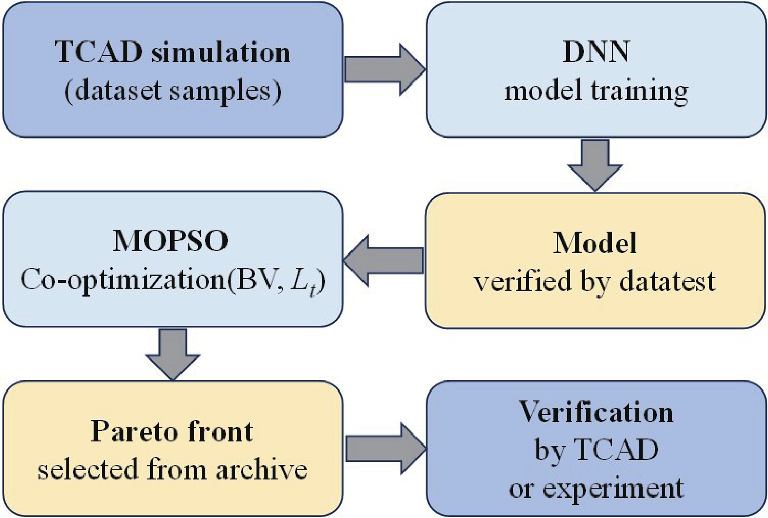
Fig. 1.
(Color online) The overall method flow of the proposed FLR optimization model.
ARTICLES
Cheng Liu, Peng Liao, Jianbin Guo, Yanghao Wang, Qingqing Sun, David Wei, Zhang and and Hang Xu
Corresponding author: Hang Xu, hang_xu@fudan.edu.cn
Abstract: Field-limiting-ring (FLR) terminations require the simultaneous optimization of multiple structural parameters, while conventional TCAD-based design is computationally expensive and often involves a trade-off between breakdown voltage (BV) and termination footprint. In this work, an area-oriented multi-objective optimization framework is developed for the FLR termination of a 650 V Si IGBT, in which BV is maximized while the total termination length (Lt) used as a geometric metric of termination-area consumption, is minimized. A deep neural network (DNN) surrogate model is trained using 420 Sentaurus TCAD samples to predict BV from the FLR structural parameters and is subsequently integrated with multi-objective particle swarm optimization (MOPSO) to construct the BV−Lt Pareto front. The DNN achieves R2 = 0.9988, a MAE of 1.5 V, and a RMSE of 1.9 V on the held-out TCAD test set. Three representative Pareto solutions are further verified by full TCAD simulations. Under nearly identical termination-length conditions, Pareto Solution 1 increases the TCAD-verified BV from 950 to 990 V, whereas under comparable BV conditions, Pareto Solution 3 reduces Lt from 290.0 to 201.9 μm, corresponding to a 30.4% reduction, while maintaining a slightly higher BV. In addition, a fabricated device based on Pareto Solution 2 exhibits close agreement between the measured and TCAD-simulated reverse I−V characteristics. These results demonstrate the effectiveness of the proposed TCAD−DNN−MOPSO framework for BV−termination-footprint co-optimization and indicate its potential extensibility to other power-device design problems.
Keywords: insulated gate bipolar transistor, termination design, deep neural network, MOPSO algorithm, Pareto front
| [1] |
Yang Y H, Dorn-Gomba L, Rodriguez R, et al. Automotive power module packaging: Current status and future trends. IEEE Access, 2020, 8: 160126 doi: 10.1109/ACCESS.2020.3019775
|
| [2] |
Lorenz L. Power semiconductor devices-development trends and system interactions. 2007 Power Conversion Conference-Nagoya, 2007: 348
|
| [3] |
Goreci L S, Popescu M, Tilă I. The choice of the IGBTs and their cooling in electric traction converters for autonomous vehicles. 2021 International Conference on Applied and Theoretical Electricity (ICATE), 2021: 1
|
| [4] |
Navarro D, Pesic I, Morikawa Y, et al. Investigation of 4H−SiC insulated-gate bipolar transistor turn-off performance for achieving low power loss. Jpn J Appl Phys, 2016, 55(4S): 04ER12 doi: 10.7567/JJAP.55.04ER12
|
| [5] |
Binder A T, Steinfeldt J, Allerman A A, et al. Optimization of step-etched junction termination extensions for vertical GaN devices. IEEE Trans Electron Devices, 2024, 71(3): 1541 doi: 10.1109/TED.2023.3344057
|
| [6] |
Huang C Y, Guo Y F, Zhang J, et al. Field plate-adaptive doping: A novel surface electric field optimization technique for SOI LDMOS with gate field plate. IEEE Trans Electron Devices, 2022, 69(1): 291 doi: 10.1109/TED.2021.3130837
|
| [7] |
Onose H, Oikawa S, Yatsuo T, et al. Over 2000 V FLR termination technologies for SiC high voltage devices. 12th International Symposium on Power Semiconductor Devices & ICs. Proceedings. Toulouse, France. IEEE, 2000: 245
|
| [8] |
Yuan J, Cheng Z J, Guo F, et al. A bottom charge-modulated field limiting rings termination with N−P−N sandwich epitaxial wafers for 4H−SiC devices. IEEE Electron Device Lett, 2025, 46(8): 1297 doi: 10.1109/LED.2025.3581587
|
| [9] |
Ji X Q, Yue J Y, Wang J J, et al. Edge-field-suppression for improved breakdown and leakage in vertical β-Ga2O3 Schottky barrier diode through trench field limiting rings. IEEE Trans Electron Devices, 2024, 71(12): 7696 doi: 10.1109/TED.2024.3484356
|
| [10] |
Zhao Y S, Li Z H, Xia Z M, et al. Enhanced filed limiting rings for improving breakdown voltage stability. 2022 IEEE 16th International Conference on Solid-State & Integrated Circuit Technology (ICSICT), 2022: 1
|
| [11] |
Ng M H, Kwok Y, Zhou W J, et al. AI-based general solution for automated TCAD parameter calibration: Case studies on TFT devices. IEEE Trans Electron Devices, 2025, 72(12): 6757 doi: 10.1109/TED.2025.3616083
|
| [12] |
Li J Y, Zhao H Y, Yuan H, et al. An innovative and efficient approach for field-limiting ring design of power devices based on deep neural networks. IEEE Electron Device Lett, 2024, 45(3): 488 doi: 10.1109/LED.2024.3352041
|
| [13] |
Hu L B, Wei X F, Shu L, et al. EMP injection for post-fabricated RON-BV optimization in bulk LDMOS and AI-assisted mechanism analysis. IEEE Electron Device Lett, 2026, 47(3): 586 doi: 10.1109/LED.2025.3649721
|
| [14] |
Yee N, Lu A, Wang Y F, et al. Rapid inverse design of GaN-on-GaN diode with guard ring termination for BV and (VFQ) −1 co-optimization. 2023 35th International Symposium on Power Semiconductor Devices and ICs (ISPSD), 2023: 143
|
| [15] |
Cao Z, Sun Q, Peng Q W, et al. Machine learning-based modeling and BV optimization for LDMOS with multifloating buried layers. IEEE Trans Electron Devices, 2025, 72(2): 550 doi: 10.1109/TED.2024.3517578
|
| [16] |
Luo R D, Sun B T, Hou X L, et al. Optimal design of 100−2000 V 4H−SiC power MOSFETs using multi-objective particle swarm optimization algorithms. IEEE Electron Device Lett, 2024, 45(5): 786 doi: 10.1109/LED.2024.3382004
|
| [17] |
Synopsys, Inc. Sentaurus Process User Guide, Version R-2020.09. Mountain View, CA: Synopsys, Inc. , 2020
|
| [18] |
Carrillo-Nuñez H, Dimitrova N, Asenov A, et al. Machine learning approach for predicting the effect of statistical variability in Si junctionless nanowire transistors. IEEE Electron Device Lett, 2019, 40(9): 1366 doi: 10.1109/LED.2019.2931839
|
| [19] |
Sola J, Sevilla J. Importance of input data normalization for the application of neural networks to complex industrial problems. IEEE Trans Nucl Sci, 1997, 44(3): 1464 doi: 10.1109/23.589532
|
| [20] |
Zhou Y T, Zhang O, Xia X, et al. Application of MOPSO algorithm to optimization of energy efficiency and spectral efficiency trade-off in massive MIMO system. 2022 IEEE International Symposium on Broadband Multimedia Systems and Broadcasting (BMSB). Bilbao, Spain. IEEE, 2022: 1
|

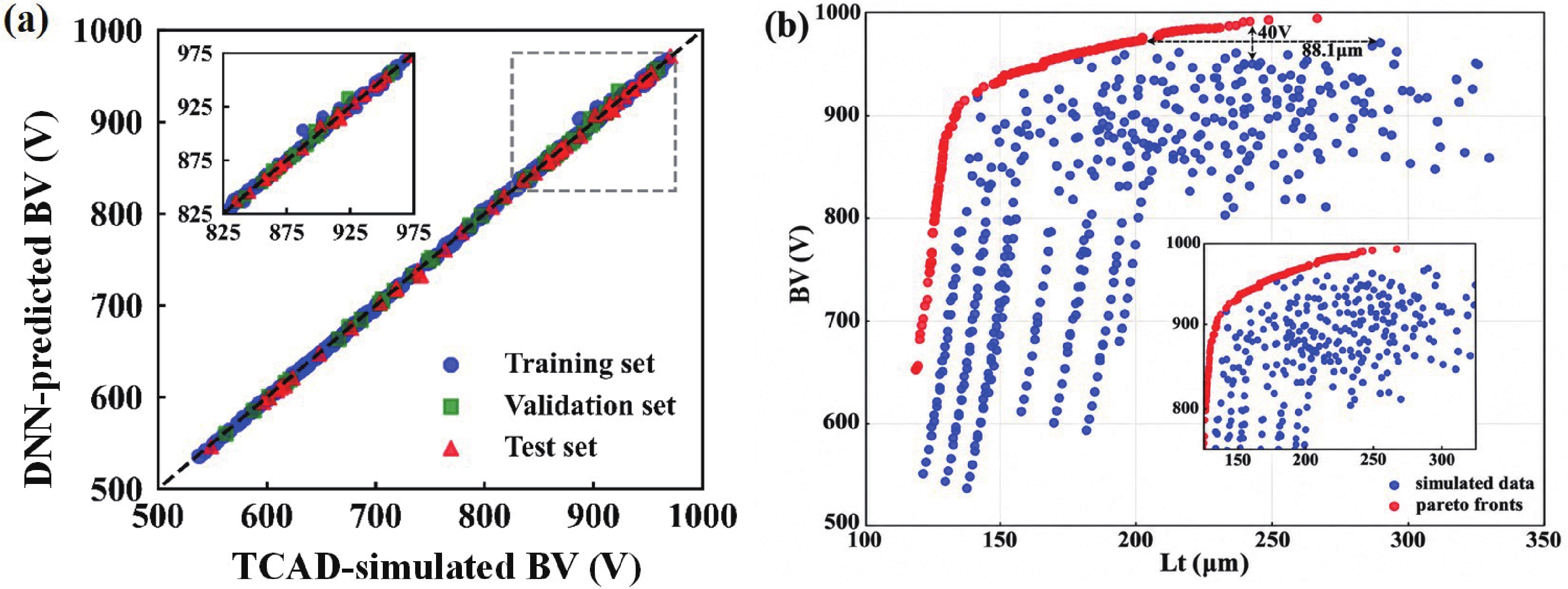
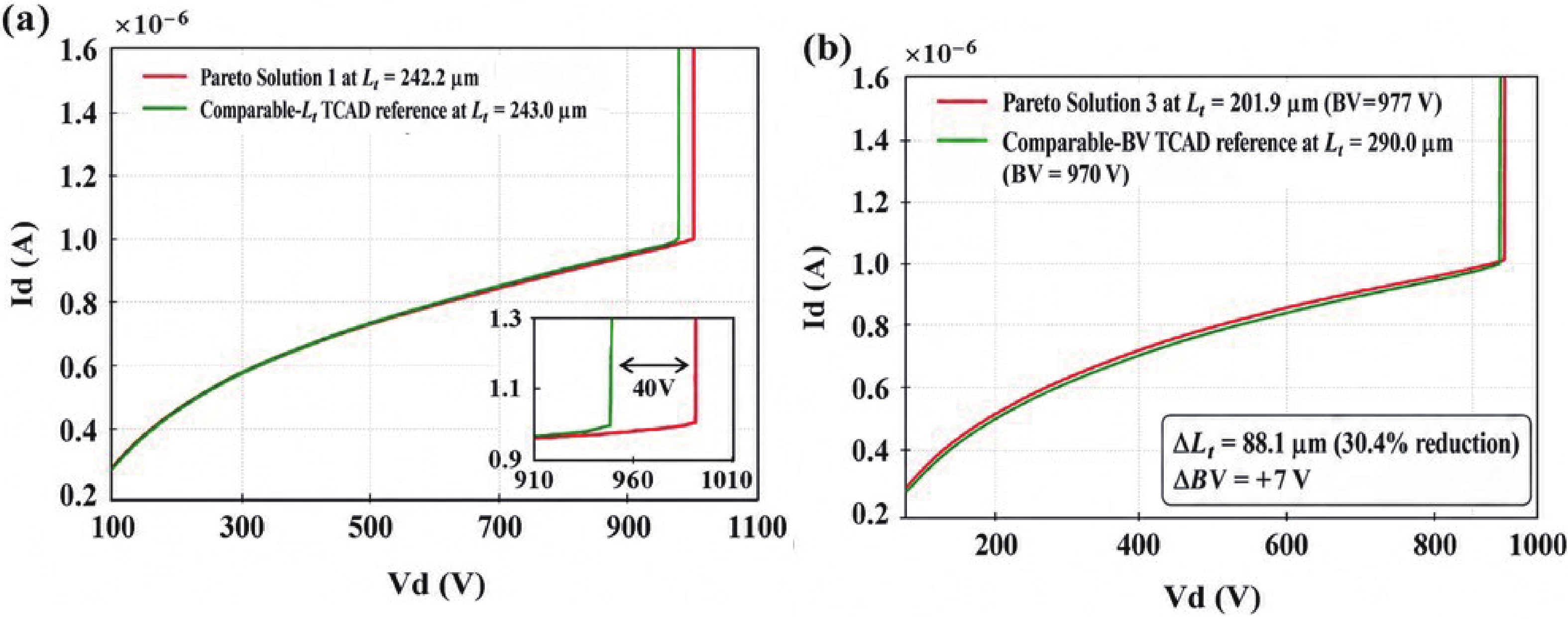
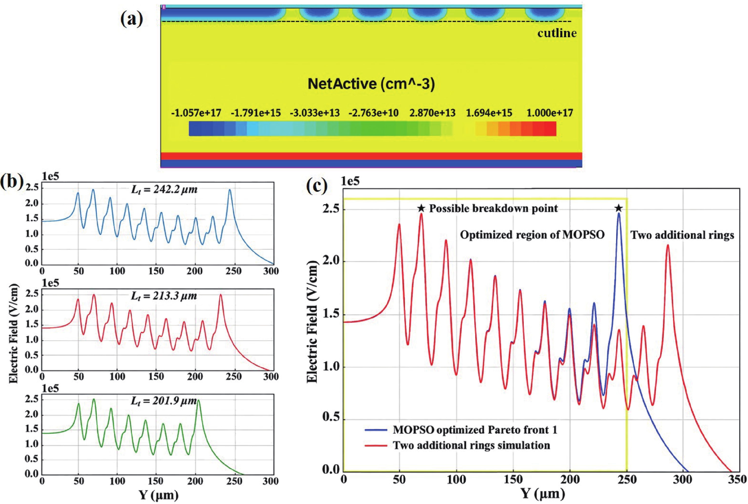
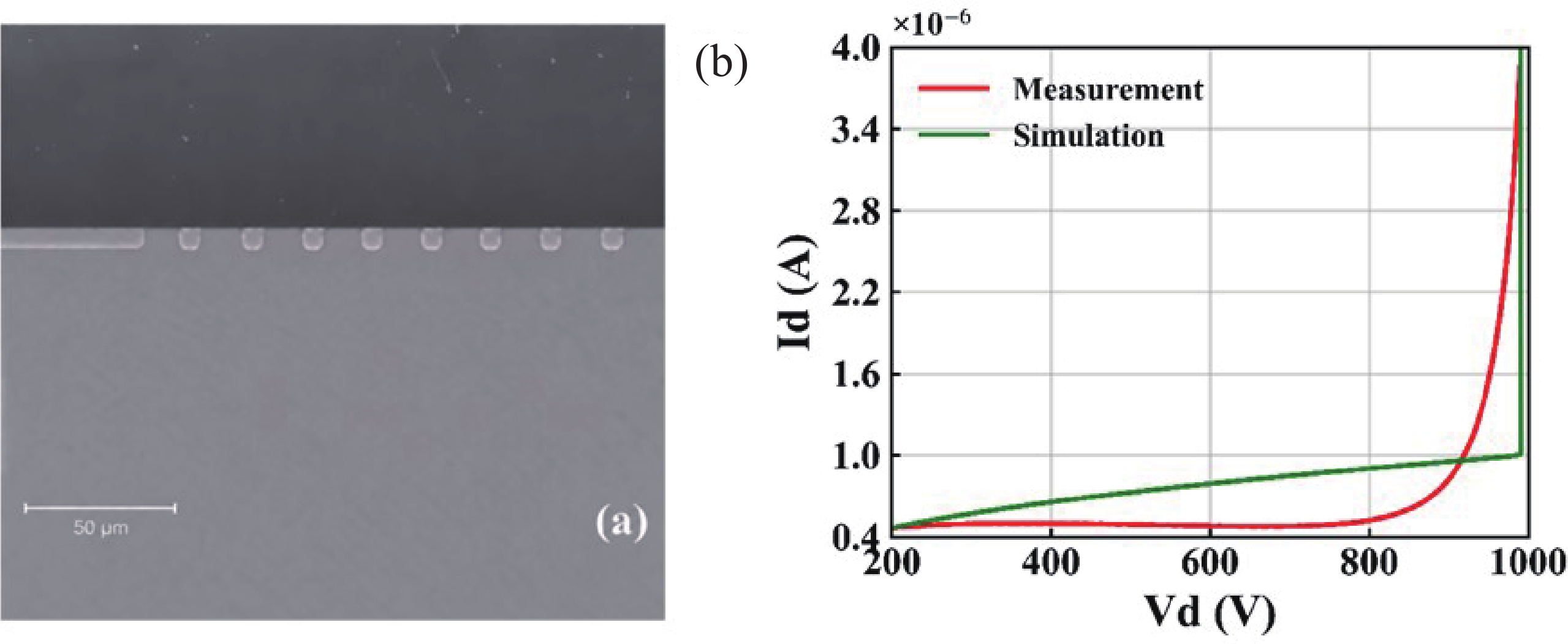
Table 1. Simulation structural parameters range.
| Input parameters | Range | Number of sampling steps | Normalization factor (n) |
| S0 (µm) | 12−18 | 7 | 0.07 |
| Si (µm) | 12−18 | 7 | |
| Wpp (µm) | 4−10 | 4 | |
| Rnum | 4−10 | 4 |
 DownLoad: CSV
Table 2. Some key algorithm parameters.
| parameters | Meaning | Range |
| w | inertia weight | 0.9−0.4 |
| c1 | cognitive parameter | 2.5−1.5 |
| c2 | social parameter | 1.5−2.5 |
DownLoad: CSV
Table 3. Selected Pareto solutions and TCAD reference samples with full TCAD validation.
| Design | S0 (μm) | Si (μm) | Wpp (μm) | Rnum | Lt (μm) | DNN BV (V) | TCAD BV (V) | BVTCAD / Lt (V/μm) |
| Pareto Solution 1 | 12.0 | 14.2 | 7.4 | 9 | 242.2 | 991 | 990 | 4.09 |
| Pareto Solution 2 | 12.1 | 14.4 | 6.3 | 8 | 213.3 | 981 | 981 | 4.60 |
| Pareto Solution 3 | 12.3 | 15.1 | 7.0 | 7 | 201.9 | 973 | 977 | 4.84 |
| Comparable-Lt TCAD reference | 15.0 | 14.0 | 10.0 | 8 | 243 | — | 950 | 3.91 |
| Comparable-BV TCAD reference | 14.0 | 14.0 | 10.0 | 10 | 290.0 | — | 970 | 3.34 |
DownLoad: CSV
Table 4. Basic structural parameters of the fabricated device corresponding to Pareto Solution 2.
| Parameters | Value |
| Cell pitch (μm) | 1.5 |
| Gate oxide thickness (nm) | 100 |
| N-drift thickness (μm) | 70 |
| FLR depth (μm) | 6 |
| Lmj (μm) | 50 |
| S0 (μm) | 12.1 |
| Si (μm) | 14.4 |
| Wpp (μm) | 6.3 |
| Rnum | 8 |
| Lt (μm) | 213.3 |
DownLoad: CSV
| [1] |
Yang Y H, Dorn-Gomba L, Rodriguez R, et al. Automotive power module packaging: Current status and future trends. IEEE Access, 2020, 8: 160126 doi: 10.1109/ACCESS.2020.3019775
|
| [2] |
Lorenz L. Power semiconductor devices-development trends and system interactions. 2007 Power Conversion Conference-Nagoya, 2007: 348
|
| [3] |
Goreci L S, Popescu M, Tilă I. The choice of the IGBTs and their cooling in electric traction converters for autonomous vehicles. 2021 International Conference on Applied and Theoretical Electricity (ICATE), 2021: 1
|
| [4] |
Navarro D, Pesic I, Morikawa Y, et al. Investigation of 4H−SiC insulated-gate bipolar transistor turn-off performance for achieving low power loss. Jpn J Appl Phys, 2016, 55(4S): 04ER12 doi: 10.7567/JJAP.55.04ER12
|
| [5] |
Binder A T, Steinfeldt J, Allerman A A, et al. Optimization of step-etched junction termination extensions for vertical GaN devices. IEEE Trans Electron Devices, 2024, 71(3): 1541 doi: 10.1109/TED.2023.3344057
|
| [6] |
Huang C Y, Guo Y F, Zhang J, et al. Field plate-adaptive doping: A novel surface electric field optimization technique for SOI LDMOS with gate field plate. IEEE Trans Electron Devices, 2022, 69(1): 291 doi: 10.1109/TED.2021.3130837
|
| [7] |
Onose H, Oikawa S, Yatsuo T, et al. Over 2000 V FLR termination technologies for SiC high voltage devices. 12th International Symposium on Power Semiconductor Devices & ICs. Proceedings. Toulouse, France. IEEE, 2000: 245
|
| [8] |
Yuan J, Cheng Z J, Guo F, et al. A bottom charge-modulated field limiting rings termination with N−P−N sandwich epitaxial wafers for 4H−SiC devices. IEEE Electron Device Lett, 2025, 46(8): 1297 doi: 10.1109/LED.2025.3581587
|
| [9] |
Ji X Q, Yue J Y, Wang J J, et al. Edge-field-suppression for improved breakdown and leakage in vertical β-Ga2O3 Schottky barrier diode through trench field limiting rings. IEEE Trans Electron Devices, 2024, 71(12): 7696 doi: 10.1109/TED.2024.3484356
|
| [10] |
Zhao Y S, Li Z H, Xia Z M, et al. Enhanced filed limiting rings for improving breakdown voltage stability. 2022 IEEE 16th International Conference on Solid-State & Integrated Circuit Technology (ICSICT), 2022: 1
|
| [11] |
Ng M H, Kwok Y, Zhou W J, et al. AI-based general solution for automated TCAD parameter calibration: Case studies on TFT devices. IEEE Trans Electron Devices, 2025, 72(12): 6757 doi: 10.1109/TED.2025.3616083
|
| [12] |
Li J Y, Zhao H Y, Yuan H, et al. An innovative and efficient approach for field-limiting ring design of power devices based on deep neural networks. IEEE Electron Device Lett, 2024, 45(3): 488 doi: 10.1109/LED.2024.3352041
|
| [13] |
Hu L B, Wei X F, Shu L, et al. EMP injection for post-fabricated RON-BV optimization in bulk LDMOS and AI-assisted mechanism analysis. IEEE Electron Device Lett, 2026, 47(3): 586 doi: 10.1109/LED.2025.3649721
|
| [14] |
Yee N, Lu A, Wang Y F, et al. Rapid inverse design of GaN-on-GaN diode with guard ring termination for BV and (VFQ) −1 co-optimization. 2023 35th International Symposium on Power Semiconductor Devices and ICs (ISPSD), 2023: 143
|
| [15] |
Cao Z, Sun Q, Peng Q W, et al. Machine learning-based modeling and BV optimization for LDMOS with multifloating buried layers. IEEE Trans Electron Devices, 2025, 72(2): 550 doi: 10.1109/TED.2024.3517578
|
| [16] |
Luo R D, Sun B T, Hou X L, et al. Optimal design of 100−2000 V 4H−SiC power MOSFETs using multi-objective particle swarm optimization algorithms. IEEE Electron Device Lett, 2024, 45(5): 786 doi: 10.1109/LED.2024.3382004
|
| [17] |
Synopsys, Inc. Sentaurus Process User Guide, Version R-2020.09. Mountain View, CA: Synopsys, Inc. , 2020
|
| [18] |
Carrillo-Nuñez H, Dimitrova N, Asenov A, et al. Machine learning approach for predicting the effect of statistical variability in Si junctionless nanowire transistors. IEEE Electron Device Lett, 2019, 40(9): 1366 doi: 10.1109/LED.2019.2931839
|
| [19] |
Sola J, Sevilla J. Importance of input data normalization for the application of neural networks to complex industrial problems. IEEE Trans Nucl Sci, 1997, 44(3): 1464 doi: 10.1109/23.589532
|
| [20] |
Zhou Y T, Zhang O, Xia X, et al. Application of MOPSO algorithm to optimization of energy efficiency and spectral efficiency trade-off in massive MIMO system. 2022 IEEE International Symposium on Broadband Multimedia Systems and Broadcasting (BMSB). Bilbao, Spain. IEEE, 2022: 1
|





Article views: 2 Times PDF downloads: 0 Times Cited by: 0 Times
Received: 10 April 2026 Revised: 10 October 2026 Online: Accepted Manuscript: 13 November 2026
| Citation: |
Cheng Liu, Peng Liao, Jianbin Guo, Yanghao Wang, Qingqing Sun, David Wei, Zhang and, Hang Xu. A termination area optimization method for 650 V IGBT based on DNN and MOPSO algorithm[J]. Journal of Semiconductors, 2026, In Press. doi: 10.1088/1674-4926/26040013
****
C Liu, P Liao, J B Guo, Y H Wang, Q Q Sun, D Wei, Z and, and H Xu, A termination area optimization method for 650 V IGBT based on DNN and MOPSO algorithm[J]. J. Semicond., 2026, accepted doi: 10.1088/1674-4926/26040013

|
 Cheng Liu received his Bachelor's degree in Microelectronics Science and Engineering from Jilin University in 2024. He is currently a Master's student at the School of Microelectronics, Fudan University. His research primarily focuses on the design and optimization of power devices assisted by deep learning
 Hang Xu received his bachelor's degree from Northwestern Polytechnical University and his Ph.D. degree from Fudan University in 2024. He is currently a postdoctoral fellow at the School of Microelectronics, Fudan University, Shanghai. His research interests include power semiconductor devices, silicon-based optoelectronic devices, and advanced CMOS process technologies
| [1] |
Yang Y H, Dorn-Gomba L, Rodriguez R, et al. Automotive power module packaging: Current status and future trends. IEEE Access, 2020, 8: 160126 doi: 10.1109/ACCESS.2020.3019775
|
| [2] |
Lorenz L. Power semiconductor devices-development trends and system interactions. 2007 Power Conversion Conference-Nagoya, 2007: 348
|
| [3] |
Goreci L S, Popescu M, Tilă I. The choice of the IGBTs and their cooling in electric traction converters for autonomous vehicles. 2021 International Conference on Applied and Theoretical Electricity (ICATE), 2021: 1
|
| [4] |
Navarro D, Pesic I, Morikawa Y, et al. Investigation of 4H−SiC insulated-gate bipolar transistor turn-off performance for achieving low power loss. Jpn J Appl Phys, 2016, 55(4S): 04ER12 doi: 10.7567/JJAP.55.04ER12
|
| [5] |
Binder A T, Steinfeldt J, Allerman A A, et al. Optimization of step-etched junction termination extensions for vertical GaN devices. IEEE Trans Electron Devices, 2024, 71(3): 1541 doi: 10.1109/TED.2023.3344057
|
| [6] |
Huang C Y, Guo Y F, Zhang J, et al. Field plate-adaptive doping: A novel surface electric field optimization technique for SOI LDMOS with gate field plate. IEEE Trans Electron Devices, 2022, 69(1): 291 doi: 10.1109/TED.2021.3130837
|
| [7] |
Onose H, Oikawa S, Yatsuo T, et al. Over 2000 V FLR termination technologies for SiC high voltage devices. 12th International Symposium on Power Semiconductor Devices & ICs. Proceedings. Toulouse, France. IEEE, 2000: 245
|
| [8] |
Yuan J, Cheng Z J, Guo F, et al. A bottom charge-modulated field limiting rings termination with N−P−N sandwich epitaxial wafers for 4H−SiC devices. IEEE Electron Device Lett, 2025, 46(8): 1297 doi: 10.1109/LED.2025.3581587
|
| [9] |
Ji X Q, Yue J Y, Wang J J, et al. Edge-field-suppression for improved breakdown and leakage in vertical β-Ga2O3 Schottky barrier diode through trench field limiting rings. IEEE Trans Electron Devices, 2024, 71(12): 7696 doi: 10.1109/TED.2024.3484356
|
| [10] |
Zhao Y S, Li Z H, Xia Z M, et al. Enhanced filed limiting rings for improving breakdown voltage stability. 2022 IEEE 16th International Conference on Solid-State & Integrated Circuit Technology (ICSICT), 2022: 1
|
| [11] |
Ng M H, Kwok Y, Zhou W J, et al. AI-based general solution for automated TCAD parameter calibration: Case studies on TFT devices. IEEE Trans Electron Devices, 2025, 72(12): 6757 doi: 10.1109/TED.2025.3616083
|
| [12] |
Li J Y, Zhao H Y, Yuan H, et al. An innovative and efficient approach for field-limiting ring design of power devices based on deep neural networks. IEEE Electron Device Lett, 2024, 45(3): 488 doi: 10.1109/LED.2024.3352041
|
| [13] |
Hu L B, Wei X F, Shu L, et al. EMP injection for post-fabricated RON-BV optimization in bulk LDMOS and AI-assisted mechanism analysis. IEEE Electron Device Lett, 2026, 47(3): 586 doi: 10.1109/LED.2025.3649721
|
| [14] |
Yee N, Lu A, Wang Y F, et al. Rapid inverse design of GaN-on-GaN diode with guard ring termination for BV and (VFQ) −1 co-optimization. 2023 35th International Symposium on Power Semiconductor Devices and ICs (ISPSD), 2023: 143
|
| [15] |
Cao Z, Sun Q, Peng Q W, et al. Machine learning-based modeling and BV optimization for LDMOS with multifloating buried layers. IEEE Trans Electron Devices, 2025, 72(2): 550 doi: 10.1109/TED.2024.3517578
|
| [16] |
Luo R D, Sun B T, Hou X L, et al. Optimal design of 100−2000 V 4H−SiC power MOSFETs using multi-objective particle swarm optimization algorithms. IEEE Electron Device Lett, 2024, 45(5): 786 doi: 10.1109/LED.2024.3382004
|
| [17] |
Synopsys, Inc. Sentaurus Process User Guide, Version R-2020.09. Mountain View, CA: Synopsys, Inc. , 2020
|
| [18] |
Carrillo-Nuñez H, Dimitrova N, Asenov A, et al. Machine learning approach for predicting the effect of statistical variability in Si junctionless nanowire transistors. IEEE Electron Device Lett, 2019, 40(9): 1366 doi: 10.1109/LED.2019.2931839
|
| [19] |
Sola J, Sevilla J. Importance of input data normalization for the application of neural networks to complex industrial problems. IEEE Trans Nucl Sci, 1997, 44(3): 1464 doi: 10.1109/23.589532
|
| [20] |
Zhou Y T, Zhang O, Xia X, et al. Application of MOPSO algorithm to optimization of energy efficiency and spectral efficiency trade-off in massive MIMO system. 2022 IEEE International Symposium on Broadband Multimedia Systems and Broadcasting (BMSB). Bilbao, Spain. IEEE, 2022: 1
|

 WeChat ID
Journal of Semiconductors © 2017 All Rights Reserved 京ICP备05085259号-2