J. Semicond. >  Just Accepted

ARTICLES

Improving the surface passivation of p-type HgCdTe by optimizing the CdTe film deposition rate

Xiaochi Tai1, 2, §, Bisong Tan1, §, Yan Chen1, 2, , Haoran Yan2, Jian Wang1, 2, Yahui Wang2, 3, Wenxin Li1, 2, Dongyang Zhao1, Hanxue Jiao2, 3, Xudong Wang2, , Junhao Chu1, 2 and Jianlu Wang1, 2, 3

+ Author Affiliations

 Corresponding author: Yan Chen, yanchen_@fudan.edu.cn; Xudong Wang, wxd0130@mail.sitp.ac.cn

DOI: 10.1088/1674-4926/26040022CSTR: 32376.14.1674-4926.26040022

PDF

Turn off MathJax

Abstract: Surface passivation is critical for HgCdTe infrared detectors. CdTe films are widely used to passivate HgCdTe surfaces owing to their close lattice match. However, achieving high-quality CdTe films for passivation remains challenging. In this study, CdTe films were deposited onto p-type HgCdTe by electron beam evaporation (EBE) at varied deposition rates, and the influence of post-deposition annealing was also assessed. Film quality and interfacial properties were evaluated by scanning electron microscopy (SEM) and capacitance–voltage (C–V) measurements. Low deposition rates without annealing produced denser, smoother films, whereas higher rates followed by annealing led to rougher surfaces. Electrically, when deposited at lowest rate without annealing, the fixed charge density reaches 1.138 × 1011 cm–2, the slow interface-state density reaches 1.067 × 1011 cm–2 and the fast interface-state density reaches 2.807 × 1010 cm–2·eV–1. These results underscore the importance of CdTe deposition-rate control for optimizing passivation of p-type HgCdTe.

Keywords: HgCdTe passivationCdTe filmsdeposition rateelectron beam evaporation


[1]
Wang X H, Wang M B, Liao Y L, et al. Molecular-beam epitaxy-grown HgCdTe infrared detector: Material physics, structure design, and device fabrication. Sci China Phys Mech Astron, 2023, 66(3): 237302 doi: 10.1007/s11433-022-2003-2
[2]
Rogalski A, Kopytko M, Hu W D, et al. Infrared HOT photodetectors: Status and outlook. Sensors, 2023, 23(17): 7564 doi: 10.3390/s23177564
[3]
Di Y X, Ba K, Wang X D, et al. Advanced architectures and emerging materials for high-operating-temperature infrared photodiodes. Adv Mater, 2025: e08115
[4]
Chen J, Chen J, Li X, et al. High-performance HgCdTe avalanche photodetector enabled with suppression of band-to-band tunneling effect in mid-wavelength infrared. npj Quantum Mater, 2021, 6: 103 doi: 10.1038/s41535-021-00409-3
[5]
Scheuermann A G, Lawrence J P, Kemp K W, et al. Design principles for maximizing photovoltage in metal-oxide-protected water-splitting photoanodes. Nat Mater, 2016, 15(1): 99 doi: 10.1038/nmat4451
[6]
Digdaya I A, Adhyaksa G W P, Trześniewski B J, et al. Interfacial engineering of metal-insulator-semiconductor junctions for efficient and stable photoelectrochemical water oxidation. Nat Commun, 2017, 8: 15968 doi: 10.1038/ncomms15968
[7]
Pal R, Malik A, Srivastav V, et al. Engineering interface composition for passivation of HgCdTe photodiodes. IEEE Trans Electron Devices, 2006, 53(11): 2727 doi: 10.1109/TED.2006.883817
[8]
Tan B, Mao J, Chen S, et al. Improved detection performance of 1280 × 1024 middle-wavelength infrared HgCdTe focal plane arrays with 10 μm pixel pitch. J Infrared Millim Waves, 2024, 43(1): 36
[9]
Makky W H, Siddiqui A, Tang C H. Growth, composition, and surface structure of Hg(1−x)CdxTe plasma oxides. J Vac Sci Technol A Vac Surf Films, 1986, 4(6): 3169
[10]
Nemirovsky Y, Burstein L. Anodic sulfide films on Hg1−xCdxTe. Appl Phys Lett, 1984, 44(4): 443
[11]
Mainzer N, Weiss E, Laser D, et al. Effects of anodic fluoro‐oxide on the thermal stability of Hg1−xCdxTe photoconductive arrays. J Vac Sci Technol A Vac Surf Films, 1989, 7(2): 460 doi: 10.1116/1.576203
[12]
Zakirov E R, Sidorov G Y, Krasnova I A, et al. HgCdTe surface passivation with low-temperature plasma-enhanced atomic layer deposited HfO2. Appl Surf Sci, 2025, 684: 161973 doi: 10.1016/j.apsusc.2024.161973
[13]
Tetyorkin V, Tsybrii Z, Tkachuk A, et al. Passivation of InSb and HgCdTe infrared photodiodes by polycrystalline CdTe. J Electron Mater, 2023, 52(11): 7337 doi: 10.1007/s11664-023-10671-9
[14]
Rogalski A. HgCdTe infrared detector material: History, status and outlook. Rep Prog Phys, 2005, 68(10): 2267 doi: 10.1088/0034-4885/68/10/R01
[15]
Sizov F, Vuichyk M, Svezhentsova K, et al. CdTe thin films as protective surface passivation to HgCdTe layers for the IR and THz detectors. Mater Sci Semicond Process, 2021, 124: 105577 doi: 10.1016/j.mssp.2020.105577
[16]
Tennant W E, Cockrum C A, Gilpin J B, et al. Key issues in HgCdTe-based focal plane arrays: An industry perspective. J Vac Sci Technol B Microelectron Nanometer Struct Process Meas Phenom, 1992, 10(4): 1359 doi: 10.1116/1.585869
[17]
Deng Y, Ying F, Cheng X G, et al. Vacuum baking effects on the IV characteristics of LWIR HgCdTe photodiodes with different passivation. 2008 Int Conf Opt Instrum Technol Microelectron Optoelectron Devices Integr, 2008, 7158: 715808
[18]
Sun T, Li Y J, Chen X G, et al. The dark current mechanism of HgCdTe photovoltaic detector passivated by different structure. Infrared Compon Appl, 2005, 5640: 26 doi: 10.1117/12.571918
[19]
Liang J S, Sun T, Li Y J, et al. Analysis of 1/f noise on LWIR HgCdTe photodiodes with different passivation. Infrared Compon Appl, 2005, 5640: 621 doi: 10.1117/12.572132
[20]
Ding R J, He L, Ye Z H, et al. A study on ALD ZnS passivation of HgCdTe IRFPAs detectors. Infrared Technology and Applications XLIV. Orlando, USA. SPIE, 2018: 72
[21]
Banerjee S, Dahal R, Bhat I B. A novel method to obtain higher deposition rates of CdTe using low temperature LPCVD for surface passivation of HgCdTe. J Electron Mater, 2015, 44(9): 3023 doi: 10.1007/s11664-015-3743-3
[22]
Pedryc A, Martychowiec A, Kociubiński A. Technology and characterization of HgCdTe photodiode with a strengthened passivation. Photonics Applications in Astronomy, Communications, Industry, and High-Energy Physics Experiments 2018. Wilga, Poland. SPIE, 2018: 145
[23]
Agnihotri O P, Musca C A, Faraone L. Current status and issues in the surface passivation technology of mercury cadmium telluride infrared detectors. Semicond Sci Technol, 1998, 13(8): 839 doi: 10.1088/0268-1242/13/8/002
[24]
Gawron W, Sobieski J, Manyk T, et al. MOCVD grown HgCdTe heterostructures for medium wave infrared detectors. Coatings, 2021, 11(5): 611 doi: 10.3390/coatings11050611
[25]
Rutkowski J, Adamiec K, Rogalski A. RF magnetron sputtering deposition of CdTe passivation on HgCdTe. Photodetectors Mater Devices III, 1998, 3287: 327
[26]
Dell J M, Antoszewski J, White J K, et al. RIE-induced n-on-p junction HgCdTe photodiodes: effects of passivant technology on bake stability. Mater Infrared Detect, 2001, 4454: 106 doi: 10.1117/12.448166
[27]
Chen J Y, Lin Y, Li L, et al. On the structural evolutionary behavior of the CdTe/HgCdTe interface during the annealing process. J Mater Res Technol, 2024, 28: 3175 doi: 10.1016/j.jmrt.2023.12.185
[28]
An S Y, Kim J S, Seo D W, et al. Passivation of HgCdTe p-n diode junction by compositionally graded HgCdTe formed by annealing in a Cd/Hg atmosphere. J Electron Mater, 2002, 31(7): 683 doi: 10.1007/s11664-002-0219-z
[29]
Bubulac L O, Tennant W E, Bajaj J, et al. Characterization of CdTe for HgCdTe surface passivation. J Electron Mater, 1995, 24(9): 1175 doi: 10.1007/BF02653071
[30]
Chu J H, Xu S C, Tang D Y. Energy gap versus alloy composition and temperature in Hg1−xCdxTe. Appl Phys Lett, 1983, 43(11): 1064 doi: 10.1063/1.94237
[31]
Yang Y H, Cheng S Y, Zhu X L, et al. Inverted perovskite solar cells with over 2, 000 h operational stability at 85 °C using fixed charge passivation. Nat Energy, 2024, 9(1): 37 doi: 10.1038/s41560-023-01377-7
[32]
Yang Y H, Cheng S Y, Yang X T, et al. Hafnium oxide interface stabilization for efficient, photothermally stable perovskite solar cells. Science, 2026, 391(6788): 926 doi: 10.1126/science.aea3339
[33]
Chen X L, Wu Z F, Xu S G, et al. Probing the electron states and metal-insulator transition mechanisms in molybdenum disulphide vertical heterostructures. Nat Commun, 2015, 6: 6088 doi: 10.1038/ncomms7088
[34]
Zhao Y F, Tripathi M, Čerņevičs K, et al. Electrical spectroscopy of defect states and their hybridization in monolayer MoS2. Nat Commun, 2023, 14: 44 doi: 10.1038/s41467-022-35651-1
[35]
Castagné R, Vapaille A. Description of the SiO2–Si interface properties by means of very low frequency MOS capacitance measurements. Surf Sci, 1971, 28(1): 157 doi: 10.1016/0039-6028(71)90092-6
[36]
Sze S M, Li Y, Ng K K. Physics of semiconductor devices. John Wiley & Sons, 2021
[37]
Cui A L, Sun C H, Wang F, et al. Electrical properties of plasma-free ultra-low-temperature ALD ZnS passivation on p-type HgCdTe. Infrared Phys Technol, 2021, 114: 103667 doi: 10.1016/j.infrared.2021.103667
[38]
Zakirov E R, Kesler V G, Sidorov G Y, et al. XPS investigation of the ALD Al2O3/HgCdTe heterointerface. Semicond Sci Technol, 2019, 34(6): 065007 doi: 10.1088/1361-6641/ab1961
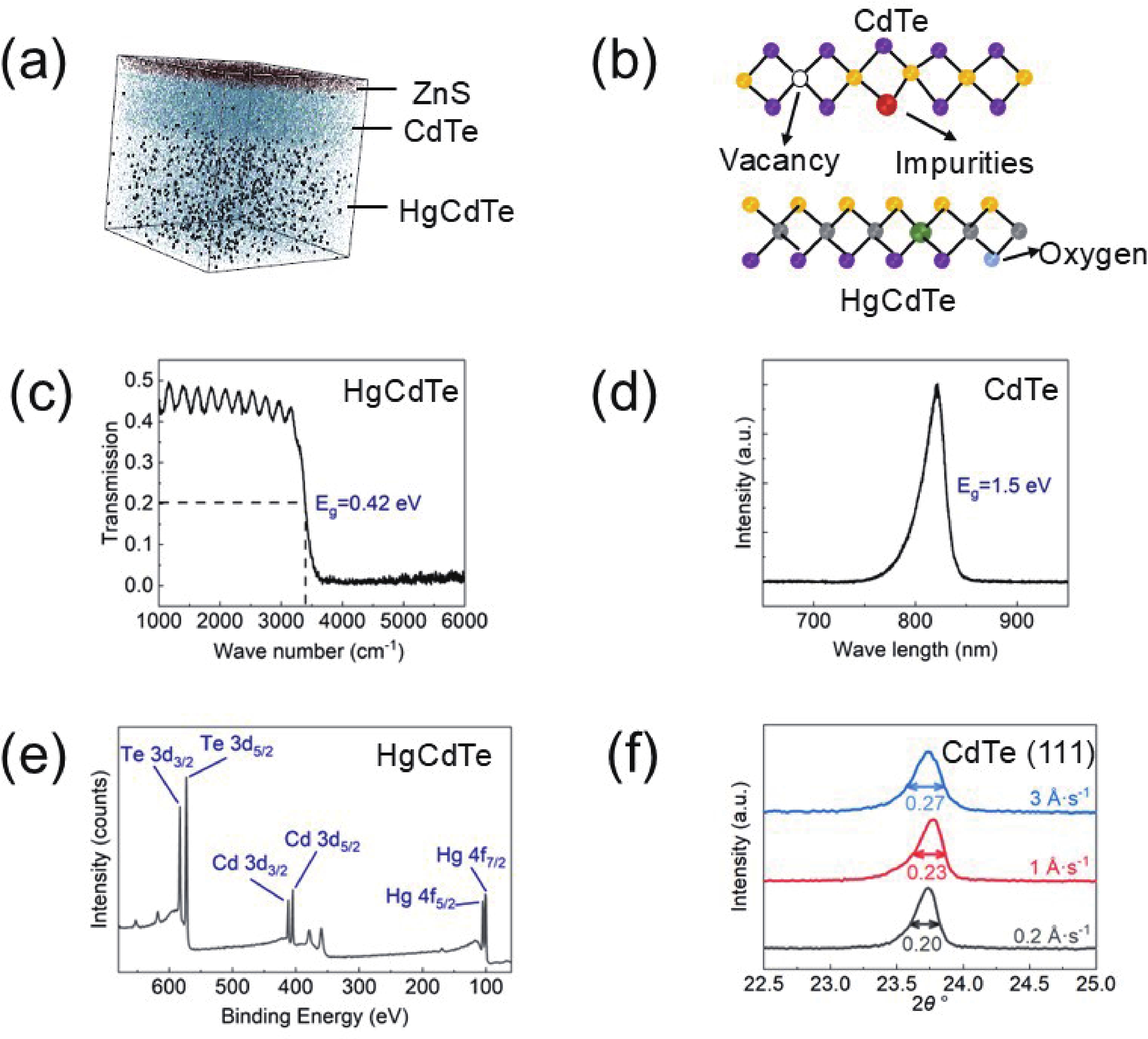
Fig. 1.  (Color online) Schematic and optical characterization of passivation structures. (a) 3D images reconstruction from ToF-SIMS depth profile experiments showing the spatial distributions of Zn+(brown), Cd+(blue), Hg+(dark) in positive ion mode. (b) Schematic representation of defects at the CdTe/HgCdTe interface. (c) Transmission spectrum of HgCdTe, showing a cutoff energy at 0.42 eV. (d) Photoluminescence (PL) spectrum of CdTe, excited by a 532 nm laser. (e) X-ray photoelectron spectroscopy (XPS) spectrum of HgCdTe surface, equipped with a monochromatic Al Kα source ( = 1486.6 eV) and a 200 μm spot size with dual charge neutralization. (f) X-ray diffraction (XRD) spectrum of CdTe deposited with different rates, FWHM of (111) are labeled.

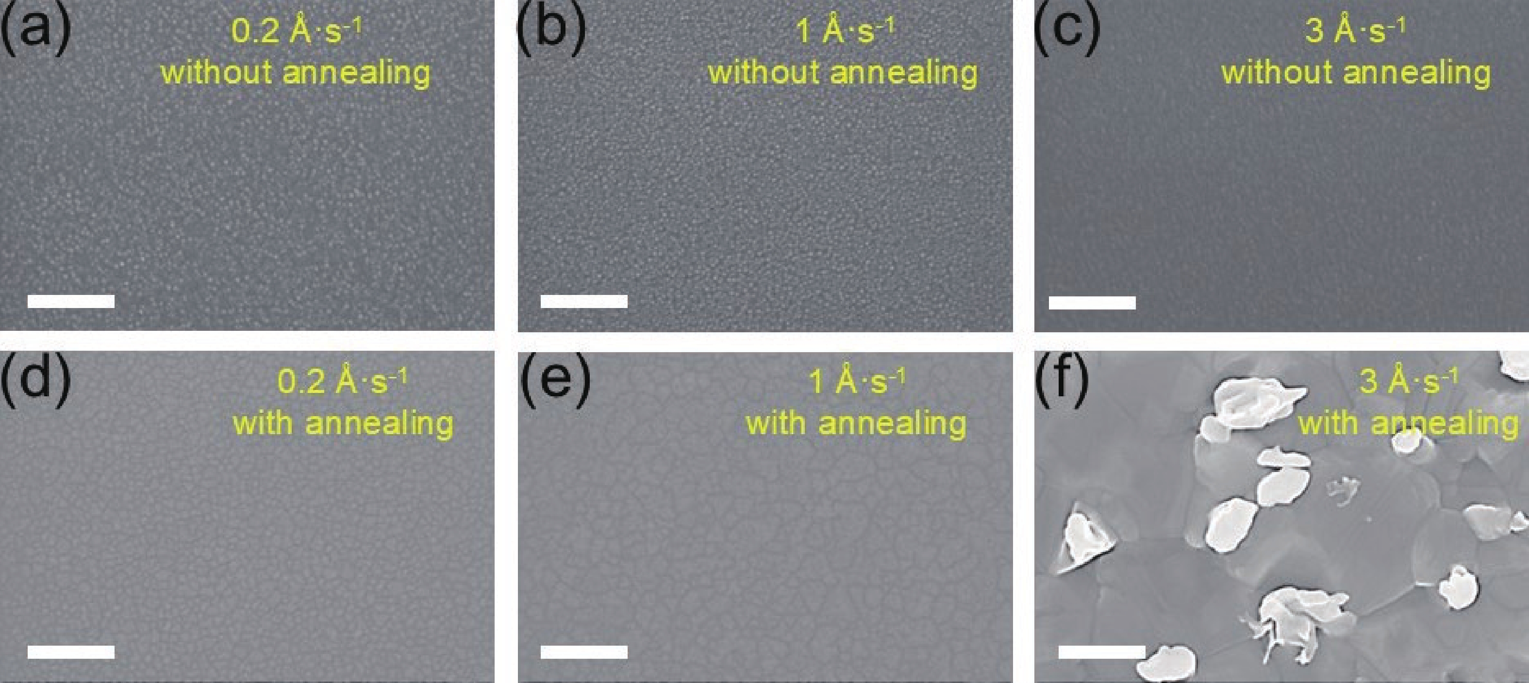
Fig. 2.  (Color online) Surface morphology of CdTe films deposited on HgCdTe. (a) 0.2 Å·s–1 without annealing, (b) 1 Å·s–1 without annealing, (c) 3 Å·s–1 without annealing, (d) 0.2 Å·s–1 with annealing, (e) 1 Å·s–1 with annealing, (f) 3 Å·s–1 with annealing. Scale bar: 200 nm.

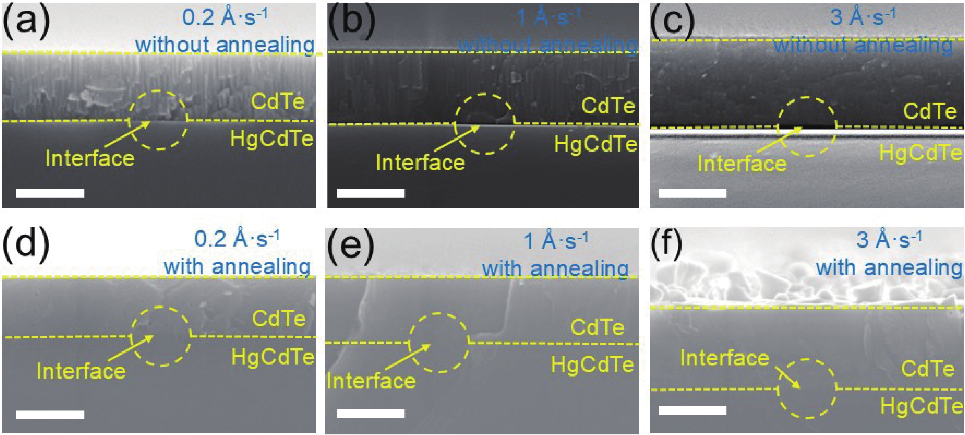
Fig. 3.  (Color online) Cross-sectional SEM analysis of CdTe/HgCdTe interfaces. (a) 0.2 Å·s–1 without annealing, (b) 1 Å·s–1 without annealing, (c) 3 Å·s–1 without annealing, (d) 0.2 Å·s–1 with annealing, (e) 1 Å·s–1 with annealing, (f) 3 Å·s–1 with annealing. Scale bar: 300 nm.

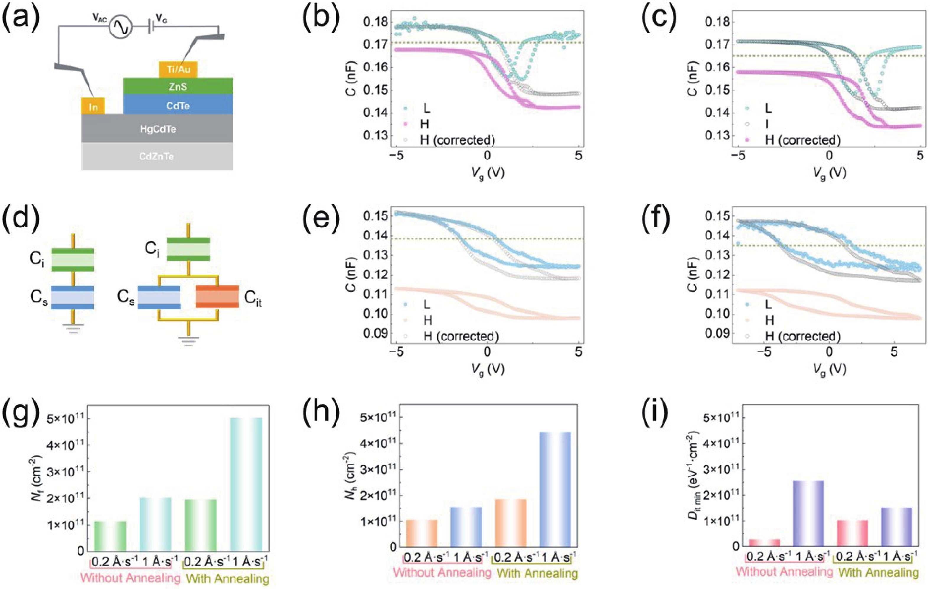
Fig. 4.  (Color online) Interface electrical properties under different passivation conditions. (a) Schematic diagram of the C–V measurement structure. (b) C–V curves of 0.2 Å·s–1 without annealing. (c) C–V curves of 1 Å·s–1 without annealing. (d) Equivalent circuit diagram for fast interface states. (e) C–V curves of 0.2 Å·s–1 with annealing. (f) C–V curves of 1 Å·s–1 with annealing. The gray dots represent the corrected high-frequency C–V curves, and the green dashed lines indicate the flat-band capacitances. (g) Fixed charge density at different deposition conditions. (h) Slow interface-state density at different deposition conditions. (i) Fast interface-state density at different deposition conditions.

Table 1.   Comparison of interface-state densities for different passivation methods.

Passivation Method$ {N}_{\text{f}} $ (cm–2)$ {N}_{\text{h}} $ (cm–2)$ {D}_{\text{it,min}} $ (cm–2·eV–1)Ref.
HgCdTe/CdTe1.138 × 10111.067 × 10112.807 × 1010This work
HgCdTe/HfO24 × 10111 × 1010[12]
HgCdTe/ZnS2.56 × 10112.36 × 10114.5 × 1011[37]
HgCdTe/CdTe (gradient)3 × 10102 × 1010[7]
HgCdTe/Al2O31 × 1012[38]
DownLoad: CSV
[1]
Wang X H, Wang M B, Liao Y L, et al. Molecular-beam epitaxy-grown HgCdTe infrared detector: Material physics, structure design, and device fabrication. Sci China Phys Mech Astron, 2023, 66(3): 237302 doi: 10.1007/s11433-022-2003-2
[2]
Rogalski A, Kopytko M, Hu W D, et al. Infrared HOT photodetectors: Status and outlook. Sensors, 2023, 23(17): 7564 doi: 10.3390/s23177564
[3]
Di Y X, Ba K, Wang X D, et al. Advanced architectures and emerging materials for high-operating-temperature infrared photodiodes. Adv Mater, 2025: e08115
[4]
Chen J, Chen J, Li X, et al. High-performance HgCdTe avalanche photodetector enabled with suppression of band-to-band tunneling effect in mid-wavelength infrared. npj Quantum Mater, 2021, 6: 103 doi: 10.1038/s41535-021-00409-3
[5]
Scheuermann A G, Lawrence J P, Kemp K W, et al. Design principles for maximizing photovoltage in metal-oxide-protected water-splitting photoanodes. Nat Mater, 2016, 15(1): 99 doi: 10.1038/nmat4451
[6]
Digdaya I A, Adhyaksa G W P, Trześniewski B J, et al. Interfacial engineering of metal-insulator-semiconductor junctions for efficient and stable photoelectrochemical water oxidation. Nat Commun, 2017, 8: 15968 doi: 10.1038/ncomms15968
[7]
Pal R, Malik A, Srivastav V, et al. Engineering interface composition for passivation of HgCdTe photodiodes. IEEE Trans Electron Devices, 2006, 53(11): 2727 doi: 10.1109/TED.2006.883817
[8]
Tan B, Mao J, Chen S, et al. Improved detection performance of 1280 × 1024 middle-wavelength infrared HgCdTe focal plane arrays with 10 μm pixel pitch. J Infrared Millim Waves, 2024, 43(1): 36
[9]
Makky W H, Siddiqui A, Tang C H. Growth, composition, and surface structure of Hg(1−x)CdxTe plasma oxides. J Vac Sci Technol A Vac Surf Films, 1986, 4(6): 3169
[10]
Nemirovsky Y, Burstein L. Anodic sulfide films on Hg1−xCdxTe. Appl Phys Lett, 1984, 44(4): 443
[11]
Mainzer N, Weiss E, Laser D, et al. Effects of anodic fluoro‐oxide on the thermal stability of Hg1−xCdxTe photoconductive arrays. J Vac Sci Technol A Vac Surf Films, 1989, 7(2): 460 doi: 10.1116/1.576203
[12]
Zakirov E R, Sidorov G Y, Krasnova I A, et al. HgCdTe surface passivation with low-temperature plasma-enhanced atomic layer deposited HfO2. Appl Surf Sci, 2025, 684: 161973 doi: 10.1016/j.apsusc.2024.161973
[13]
Tetyorkin V, Tsybrii Z, Tkachuk A, et al. Passivation of InSb and HgCdTe infrared photodiodes by polycrystalline CdTe. J Electron Mater, 2023, 52(11): 7337 doi: 10.1007/s11664-023-10671-9
[14]
Rogalski A. HgCdTe infrared detector material: History, status and outlook. Rep Prog Phys, 2005, 68(10): 2267 doi: 10.1088/0034-4885/68/10/R01
[15]
Sizov F, Vuichyk M, Svezhentsova K, et al. CdTe thin films as protective surface passivation to HgCdTe layers for the IR and THz detectors. Mater Sci Semicond Process, 2021, 124: 105577 doi: 10.1016/j.mssp.2020.105577
[16]
Tennant W E, Cockrum C A, Gilpin J B, et al. Key issues in HgCdTe-based focal plane arrays: An industry perspective. J Vac Sci Technol B Microelectron Nanometer Struct Process Meas Phenom, 1992, 10(4): 1359 doi: 10.1116/1.585869
[17]
Deng Y, Ying F, Cheng X G, et al. Vacuum baking effects on the IV characteristics of LWIR HgCdTe photodiodes with different passivation. 2008 Int Conf Opt Instrum Technol Microelectron Optoelectron Devices Integr, 2008, 7158: 715808
[18]
Sun T, Li Y J, Chen X G, et al. The dark current mechanism of HgCdTe photovoltaic detector passivated by different structure. Infrared Compon Appl, 2005, 5640: 26 doi: 10.1117/12.571918
[19]
Liang J S, Sun T, Li Y J, et al. Analysis of 1/f noise on LWIR HgCdTe photodiodes with different passivation. Infrared Compon Appl, 2005, 5640: 621 doi: 10.1117/12.572132
[20]
Ding R J, He L, Ye Z H, et al. A study on ALD ZnS passivation of HgCdTe IRFPAs detectors. Infrared Technology and Applications XLIV. Orlando, USA. SPIE, 2018: 72
[21]
Banerjee S, Dahal R, Bhat I B. A novel method to obtain higher deposition rates of CdTe using low temperature LPCVD for surface passivation of HgCdTe. J Electron Mater, 2015, 44(9): 3023 doi: 10.1007/s11664-015-3743-3
[22]
Pedryc A, Martychowiec A, Kociubiński A. Technology and characterization of HgCdTe photodiode with a strengthened passivation. Photonics Applications in Astronomy, Communications, Industry, and High-Energy Physics Experiments 2018. Wilga, Poland. SPIE, 2018: 145
[23]
Agnihotri O P, Musca C A, Faraone L. Current status and issues in the surface passivation technology of mercury cadmium telluride infrared detectors. Semicond Sci Technol, 1998, 13(8): 839 doi: 10.1088/0268-1242/13/8/002
[24]
Gawron W, Sobieski J, Manyk T, et al. MOCVD grown HgCdTe heterostructures for medium wave infrared detectors. Coatings, 2021, 11(5): 611 doi: 10.3390/coatings11050611
[25]
Rutkowski J, Adamiec K, Rogalski A. RF magnetron sputtering deposition of CdTe passivation on HgCdTe. Photodetectors Mater Devices III, 1998, 3287: 327
[26]
Dell J M, Antoszewski J, White J K, et al. RIE-induced n-on-p junction HgCdTe photodiodes: effects of passivant technology on bake stability. Mater Infrared Detect, 2001, 4454: 106 doi: 10.1117/12.448166
[27]
Chen J Y, Lin Y, Li L, et al. On the structural evolutionary behavior of the CdTe/HgCdTe interface during the annealing process. J Mater Res Technol, 2024, 28: 3175 doi: 10.1016/j.jmrt.2023.12.185
[28]
An S Y, Kim J S, Seo D W, et al. Passivation of HgCdTe p-n diode junction by compositionally graded HgCdTe formed by annealing in a Cd/Hg atmosphere. J Electron Mater, 2002, 31(7): 683 doi: 10.1007/s11664-002-0219-z
[29]
Bubulac L O, Tennant W E, Bajaj J, et al. Characterization of CdTe for HgCdTe surface passivation. J Electron Mater, 1995, 24(9): 1175 doi: 10.1007/BF02653071
[30]
Chu J H, Xu S C, Tang D Y. Energy gap versus alloy composition and temperature in Hg1−xCdxTe. Appl Phys Lett, 1983, 43(11): 1064 doi: 10.1063/1.94237
[31]
Yang Y H, Cheng S Y, Zhu X L, et al. Inverted perovskite solar cells with over 2, 000 h operational stability at 85 °C using fixed charge passivation. Nat Energy, 2024, 9(1): 37 doi: 10.1038/s41560-023-01377-7
[32]
Yang Y H, Cheng S Y, Yang X T, et al. Hafnium oxide interface stabilization for efficient, photothermally stable perovskite solar cells. Science, 2026, 391(6788): 926 doi: 10.1126/science.aea3339
[33]
Chen X L, Wu Z F, Xu S G, et al. Probing the electron states and metal-insulator transition mechanisms in molybdenum disulphide vertical heterostructures. Nat Commun, 2015, 6: 6088 doi: 10.1038/ncomms7088
[34]
Zhao Y F, Tripathi M, Čerņevičs K, et al. Electrical spectroscopy of defect states and their hybridization in monolayer MoS2. Nat Commun, 2023, 14: 44 doi: 10.1038/s41467-022-35651-1
[35]
Castagné R, Vapaille A. Description of the SiO2–Si interface properties by means of very low frequency MOS capacitance measurements. Surf Sci, 1971, 28(1): 157 doi: 10.1016/0039-6028(71)90092-6
[36]
Sze S M, Li Y, Ng K K. Physics of semiconductor devices. John Wiley & Sons, 2021
[37]
Cui A L, Sun C H, Wang F, et al. Electrical properties of plasma-free ultra-low-temperature ALD ZnS passivation on p-type HgCdTe. Infrared Phys Technol, 2021, 114: 103667 doi: 10.1016/j.infrared.2021.103667
[38]
Zakirov E R, Kesler V G, Sidorov G Y, et al. XPS investigation of the ALD Al2O3/HgCdTe heterointerface. Semicond Sci Technol, 2019, 34(6): 065007 doi: 10.1088/1361-6641/ab1961
  • Search

    Advanced Search >>

    GET CITATION

    shu

    Export: BibTex EndNote

    Article Metrics

    Article views: 2 Times PDF downloads: 0 Times Cited by: 0 Times

    History

    Received: 14 April 2026 Revised: 03 July 2026 Online: Accepted Manuscript: 13 August 2026

    Catalog

      Email This Article

      User name:
      Email:*请输入正确邮箱
      Code:*验证码错误
      Xiaochi Tai, Bisong Tan, Yan Chen, Haoran Yan, Jian Wang, Yahui Wang, Wenxin Li, Dongyang Zhao, Hanxue Jiao, Xudong Wang, Junhao Chu, Jianlu Wang. Improving the surface passivation of p-type HgCdTe by optimizing the CdTe film deposition rate[J]. Journal of Semiconductors, 2026, In Press. doi: 10.1088/1674-4926/26040022 ****X C Tai, B S Tan, Y Chen, H R Yan, J Wang, Y H Wang, W X Li, D Y Zhao, H X Jiao, X D Wang, J H Chu, and J L Wang, Improving the surface passivation of p-type HgCdTe by optimizing the CdTe film deposition rate[J]. J. Semicond., 2026, accepted doi: 10.1088/1674-4926/26040022
      Citation:
      Xiaochi Tai, Bisong Tan, Yan Chen, Haoran Yan, Jian Wang, Yahui Wang, Wenxin Li, Dongyang Zhao, Hanxue Jiao, Xudong Wang, Junhao Chu, Jianlu Wang. Improving the surface passivation of p-type HgCdTe by optimizing the CdTe film deposition rate[J]. Journal of Semiconductors, 2026, In Press. doi: 10.1088/1674-4926/26040022 ****
      X C Tai, B S Tan, Y Chen, H R Yan, J Wang, Y H Wang, W X Li, D Y Zhao, H X Jiao, X D Wang, J H Chu, and J L Wang, Improving the surface passivation of p-type HgCdTe by optimizing the CdTe film deposition rate[J]. J. Semicond., 2026, accepted doi: 10.1088/1674-4926/26040022

      Improving the surface passivation of p-type HgCdTe by optimizing the CdTe film deposition rate

      DOI: 10.1088/1674-4926/26040022
      CSTR: 32376.14.1674-4926.26040022
      More Information

      Catalog

        /

        DownLoad:  Full-Size Img  PowerPoint
        Return
        Return