


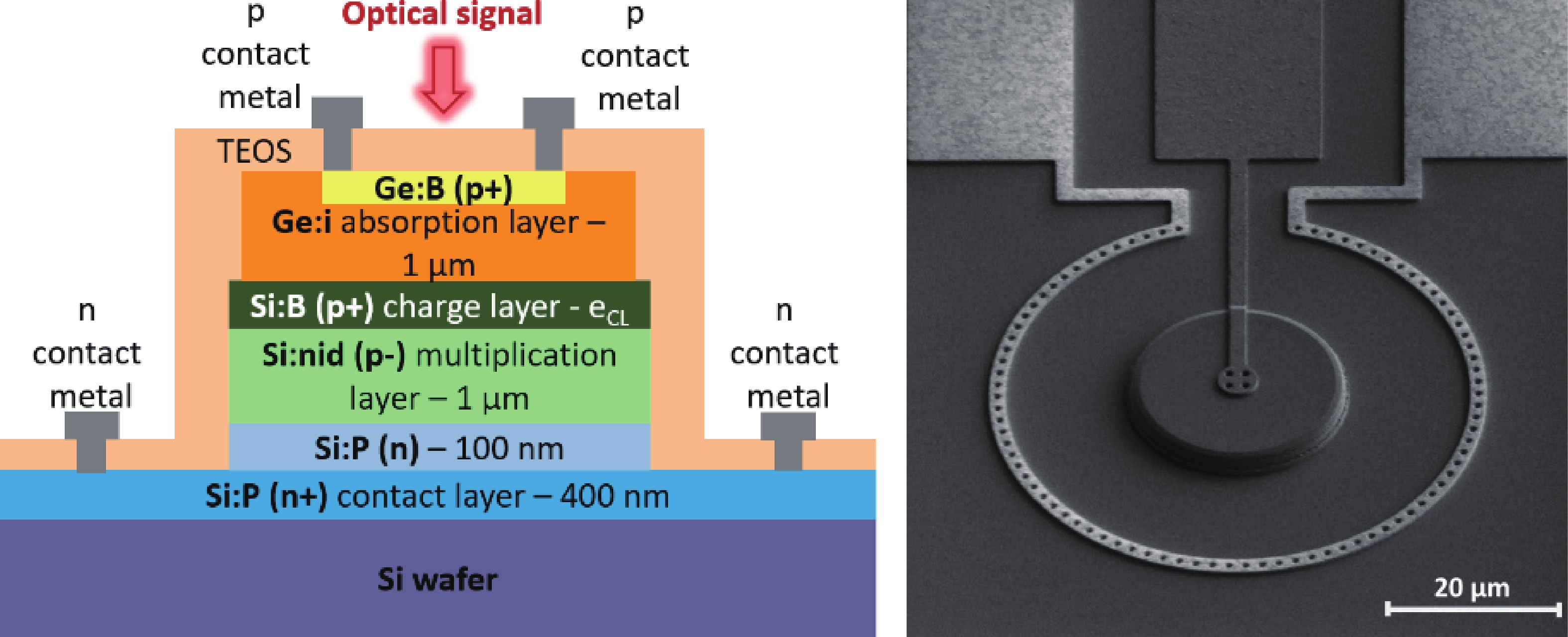
Fig. 1.
(Color online) (a) Schematic representation of the Ge−on−Si APD device. (b) SEM top view of the device.
ARTICLES
C. Latargez, T. Guerra, Q. Durlin, C. Vialle, M. Le Cocq, J-M. Hartmann, J. Rothman, L. André and A. Aliane
Corresponding author: A. Aliane, abdelkader.aliane@cea.fr
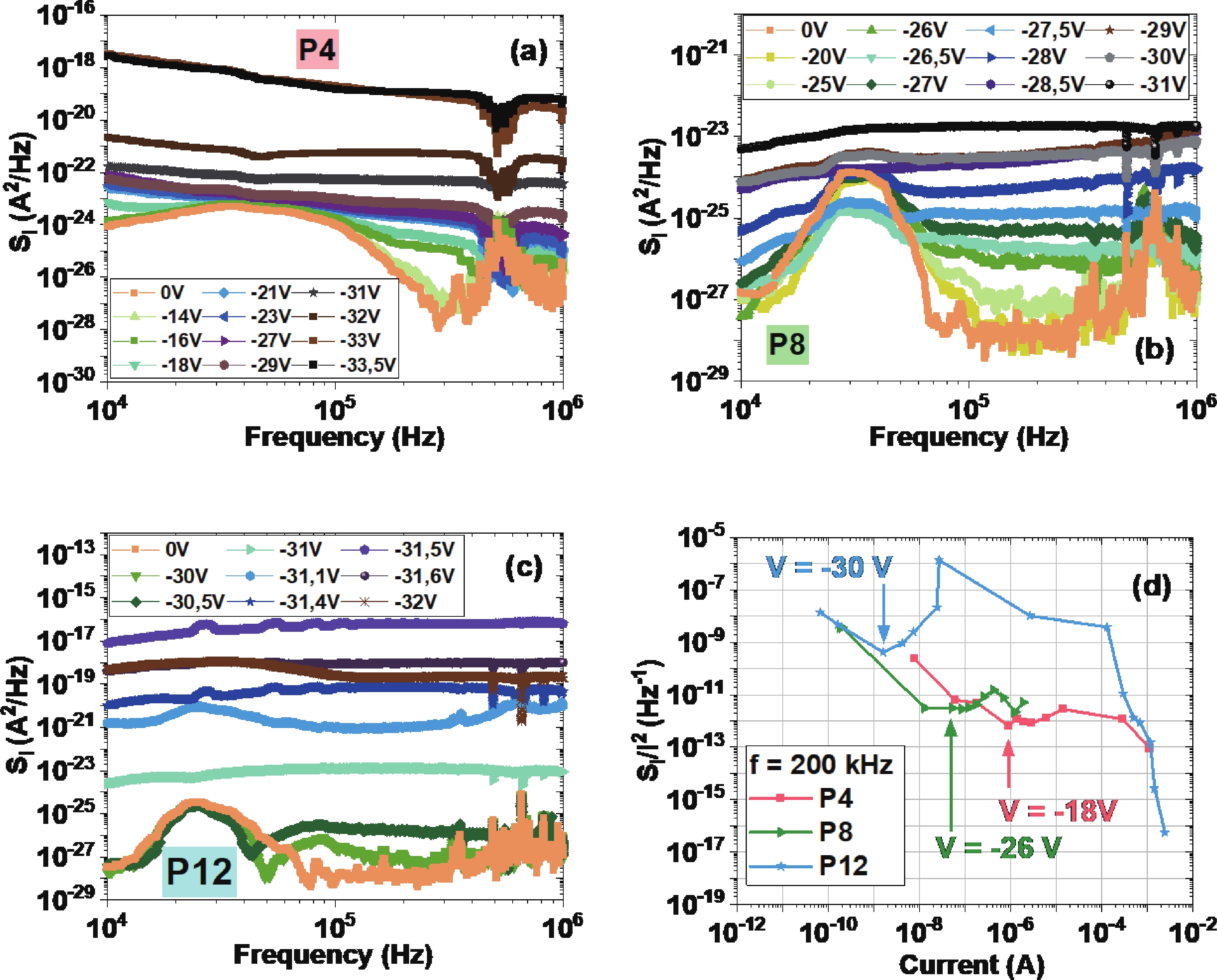
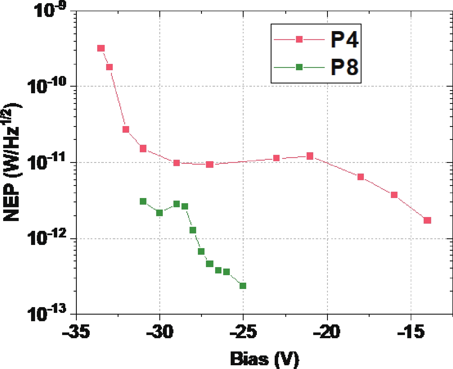
Abstract: Germanium−on−Silicon (Ge−on−Si) Avalanche Photodiodes (APDs) have attracted significant interest for LIDAR sensor applications over the last decade. However, further improvements are still needed to reduce dark current and excess noise while increasing the gain to fit the application requirements. Moreover, designing a good charge layer in separate absorption, charge and multiplication (SACM) structure for an APD is essential to control the electric field intensity in both the multiplication layer and germanium absorption layer. In this study, three different silicon charge layer thicknesses (80, 100, and 120 nm) and two boron doping concentrations of 2.5$ \times $1017 at.cm−3 and 5$ \times $1017 at.cm−3 were fabricated and characterized in vertical Ge−on−Si APDs. Our investigation focuses on the boron concentration of 2.5$ \times $1017 at.cm−3 to identify the physical contributions to current and noise at room temperature and a wavelength of 1550 nm. The device with a charge layer thickness of 80 nm exhibits the lowest equivalent input noise (NEI) of 1.7 pA/√Hz at a gain of 4.1, which is compatible with LIDAR application requirements. The results indicate that there may be an optimal combination of charge layer thickness and doping concentration for minimizing APD noise, which should be considered in future APD designs.
Keywords: avalanche photodiode, germanium, short-wave infrared, noise measurements, lidar.
| [1] |
Piron F, Morrison D, Yuce M R, et al. A review of single-photon avalanche diode time-of-flight imaging sensor arrays. IEEE Sens J, 2021, 21(11): 12654 doi: 10.1109/JSEN.2020.3039362
|
| [2] |
Campbell J C. Recent advances in telecommunications avalanche photodiodes. J Lightwave Technol, 2007, 25(1): 109 doi: 10.1109/JLT.2006.888481
|
| [3] |
Lu Z W, Kang Y M, Hu C, et al. Geiger-mode operation of Ge-on-Si avalanche photodiodes. IEEE J Quantum Electron, 2011, 47(5): 731 doi: 10.1109/JQE.2011.2110637
|
| [4] |
Huang M Y, Li S, Cai P F, et al. Germanium on silicon avalanche photodiode. IEEE J Sel Top Quantum Electron, 2018, 24(2): 1
|
| [5] |
Virot L, Crozat P, Fédéli J M, et al. Germanium avalanche receiver for low power interconnects. Nat Commun, 2014, 5: 4957 doi: 10.1038/ncomms5957
|
| [6] |
Kang Y M, Liu H D, Morse M, et al. Monolithic germanium/silicon avalanche photodiodes with 340 GHz gain–bandwidth product. Nature Photon, 2009, 3(1): 59 doi: 10.1038/nphoton.2008.247
|
| [7] |
Pellegrini S, Warburton R E, Tan L J J, et al. Design and performance of an InGaAs–InP single-photon avalanche diode detector. IEEE J Quantum Electron, 2006, 42(4): 397 doi: 10.1109/JQE.2006.871067
|
| [8] |
Zhang J, Itzler M A, Zbinden H, et al. Advances in InGaAs/InP single-photon detector systems for quantum communication. Light Sci Appl, 2015, 4(5): e286 doi: 10.1038/lsa.2015.59
|
| [9] |
Xie S Y, Zhou X X, Zhang S Y, et al. InGaAs/AlGaAsSb avalanche photodiode with high gain-bandwidth product. Opt Express, 2016, 24(21): 24242 doi: 10.1364/OE.24.024242
|
| [10] |
Na N, Lu Y-C, Liu Y-H, et al. Room temperature operation of germanium–silicon single-photon avalanche diode. Nature, 2024, 627: 295-300 doi: 10.1038/s41586-024-07076-x
|
| [11] |
Latargez C, Durlin Q, Vialle C, et al. Study of Ge-on-Si avalanche photodiodes for short-wave infrared applications. Semicond Sci Technol, 2025, 40(3): 035014 doi: 10.1088/1361-6641/adb87e
|
| [12] |
Victory Device User Manual, Silvaco, Inc. (available at: www.silvaco.com)
|
| [13] |
Fleming F, Yi X, Mirza M M A, et al. Surface-normal illuminated pseudo-planar Ge-on-Si avalanche photodiodes with high gain and low noise. Opt Express, 2024, 32(11): 19449 doi: 10.1364/OE.521417
|
| [14] |
Durlin Q, Aliane A, André L, et al. Fabrication and characterisation of the PiN Ge photodiode with poly-crystalline Si: P as n-type region. Opto Electron Rev, 2023: 144550
|
| [15] |
Guo Z L, Wang W J, Li Y J, et al. Material defects and dark currents in InGaAs/InP avalanche photodiode devices. IEEE Trans Electron Devices, 2022, 69(9): 4944 doi: 10.1109/TED.2022.3188242
|
| [16] |
Rothman J, Guerra T, Abergel J, et al. High operating temperature performance characterization of SWIR HgCdTe avalanche photodiodes. J Electron Mater, 2025, 54(10): 8323 doi: 10.1007/s11664-025-12133-w
|
| [17] |
Cao J, Wang H, You H, et al. Temperature dependent low-frequency noise characteristics of AlGaN avalanche photodiodes with ultra-shallow bevel edge termination. Journal of Alloys and Compounds, 2025, 1010: 177934 doi: 10.1016/j.jallcom.2024.177934
|
| [18] |
Chen C-E, Huang S M, Wang T J, et al. High temperature tolerant Ge-on-Si single photon avalanche diode at the communication wavelength. IEEE Electron Device Lett, 2024, 45(8): 1413 doi: 10.1109/LED.2024.3416186
|
| [19] |
Warburton R E, Intermite G, Myronov M, et al. Ge-on-Si single-photon avalanche diode detectors: Design, modeling, fabrication, and characterization at wavelengths 1310 and 1550 nm. IEEE Trans Electron Devices, 2013, 60(11): 3807 doi: 10.1109/TED.2013.2282712
|
| [20] |
Vines P, Kuzmenko K, Kirdoda J, et al. High performance planar germanium-on-silicon single-photon avalanche diode detectors. Nat Commun, 2019, 10: 1086 doi: 10.1038/s41467-019-08830-w
|


Article views: 12 Times PDF downloads: 0 Times Cited by: 0 Times
Received: 24 April 2026 Revised: 28 May 2026 Online: Accepted Manuscript: 26 June 2026
| Citation: |
C. Latargez, T. Guerra, Q. Durlin, C. Vialle, M. Le Cocq, J-M. Hartmann, J. Rothman, L. André, A. Aliane. Impact of charge layer thickness on current and noise in Ge−on−Si avalanche photodiodes at 1550 nm for lidar applications[J]. Journal of Semiconductors, 2026, In Press. doi: 10.1088/1674-4926/26040044
****
C. Latargez, T. Guerra, Q. Durlin, C. Vialle, M. Le Cocq, J-M. Hartmann, J. Rothman, L. André, and A. Aliane, Impact of charge layer thickness on current and noise in Ge−on−Si avalanche photodiodes at 1550 nm for lidar applications[J]. J. Semicond., 2026, accepted doi: 10.1088/1674-4926/26040044

|
 C. Latargez:Charlotte Latargez got her bachelor’s degree in 2018 and her master’s degree in 2020 from University Grenoble Alpes. In 2023, she joined CEA-LETI as an electro-optical characterization engineer, where she worked on germanium detectors for SWIR detection. Now she is a research engineer at the Néel Institute Grenoble. Her work focuses on the fabrication and characterization of infrared detectors, ranging from SWIR to LWIR, including photodiodes and thermoelectric detectors
 A. Aliane:Abdelkader Aliane received the M.S. degree in 2005 from University of Toulouse III – Paul Sabatier and SUPAERO, France, and the Ph.D. degree in micro- and nanoelectronics from Grenoble Institute of Technology in 2009. In 2010, he joined Sherbrooke University, Canada, as a postdoctoral researcher, where he worked on cooled germanium bolometers for X-ray detection. In 2011, he joined CEA-LITEN as a research engineer, working on printed organic devices. In 2014, he joined CEA-LETI, where he currently works. His research interests focus on advanced microbolometers for terahertz and infrared detection
| [1] |
Piron F, Morrison D, Yuce M R, et al. A review of single-photon avalanche diode time-of-flight imaging sensor arrays. IEEE Sens J, 2021, 21(11): 12654 doi: 10.1109/JSEN.2020.3039362
|
| [2] |
Campbell J C. Recent advances in telecommunications avalanche photodiodes. J Lightwave Technol, 2007, 25(1): 109 doi: 10.1109/JLT.2006.888481
|
| [3] |
Lu Z W, Kang Y M, Hu C, et al. Geiger-mode operation of Ge-on-Si avalanche photodiodes. IEEE J Quantum Electron, 2011, 47(5): 731 doi: 10.1109/JQE.2011.2110637
|
| [4] |
Huang M Y, Li S, Cai P F, et al. Germanium on silicon avalanche photodiode. IEEE J Sel Top Quantum Electron, 2018, 24(2): 1
|
| [5] |
Virot L, Crozat P, Fédéli J M, et al. Germanium avalanche receiver for low power interconnects. Nat Commun, 2014, 5: 4957 doi: 10.1038/ncomms5957
|
| [6] |
Kang Y M, Liu H D, Morse M, et al. Monolithic germanium/silicon avalanche photodiodes with 340 GHz gain–bandwidth product. Nature Photon, 2009, 3(1): 59 doi: 10.1038/nphoton.2008.247
|
| [7] |
Pellegrini S, Warburton R E, Tan L J J, et al. Design and performance of an InGaAs–InP single-photon avalanche diode detector. IEEE J Quantum Electron, 2006, 42(4): 397 doi: 10.1109/JQE.2006.871067
|
| [8] |
Zhang J, Itzler M A, Zbinden H, et al. Advances in InGaAs/InP single-photon detector systems for quantum communication. Light Sci Appl, 2015, 4(5): e286 doi: 10.1038/lsa.2015.59
|
| [9] |
Xie S Y, Zhou X X, Zhang S Y, et al. InGaAs/AlGaAsSb avalanche photodiode with high gain-bandwidth product. Opt Express, 2016, 24(21): 24242 doi: 10.1364/OE.24.024242
|
| [10] |
Na N, Lu Y-C, Liu Y-H, et al. Room temperature operation of germanium–silicon single-photon avalanche diode. Nature, 2024, 627: 295-300 doi: 10.1038/s41586-024-07076-x
|
| [11] |
Latargez C, Durlin Q, Vialle C, et al. Study of Ge-on-Si avalanche photodiodes for short-wave infrared applications. Semicond Sci Technol, 2025, 40(3): 035014 doi: 10.1088/1361-6641/adb87e
|
| [12] |
Victory Device User Manual, Silvaco, Inc. (available at: www.silvaco.com)
|
| [13] |
Fleming F, Yi X, Mirza M M A, et al. Surface-normal illuminated pseudo-planar Ge-on-Si avalanche photodiodes with high gain and low noise. Opt Express, 2024, 32(11): 19449 doi: 10.1364/OE.521417
|
| [14] |
Durlin Q, Aliane A, André L, et al. Fabrication and characterisation of the PiN Ge photodiode with poly-crystalline Si: P as n-type region. Opto Electron Rev, 2023: 144550
|
| [15] |
Guo Z L, Wang W J, Li Y J, et al. Material defects and dark currents in InGaAs/InP avalanche photodiode devices. IEEE Trans Electron Devices, 2022, 69(9): 4944 doi: 10.1109/TED.2022.3188242
|
| [16] |
Rothman J, Guerra T, Abergel J, et al. High operating temperature performance characterization of SWIR HgCdTe avalanche photodiodes. J Electron Mater, 2025, 54(10): 8323 doi: 10.1007/s11664-025-12133-w
|
| [17] |
Cao J, Wang H, You H, et al. Temperature dependent low-frequency noise characteristics of AlGaN avalanche photodiodes with ultra-shallow bevel edge termination. Journal of Alloys and Compounds, 2025, 1010: 177934 doi: 10.1016/j.jallcom.2024.177934
|
| [18] |
Chen C-E, Huang S M, Wang T J, et al. High temperature tolerant Ge-on-Si single photon avalanche diode at the communication wavelength. IEEE Electron Device Lett, 2024, 45(8): 1413 doi: 10.1109/LED.2024.3416186
|
| [19] |
Warburton R E, Intermite G, Myronov M, et al. Ge-on-Si single-photon avalanche diode detectors: Design, modeling, fabrication, and characterization at wavelengths 1310 and 1550 nm. IEEE Trans Electron Devices, 2013, 60(11): 3807 doi: 10.1109/TED.2013.2282712
|
| [20] |
Vines P, Kuzmenko K, Kirdoda J, et al. High performance planar germanium-on-silicon single-photon avalanche diode detectors. Nat Commun, 2019, 10: 1086 doi: 10.1038/s41467-019-08830-w
|

 WeChat ID
Journal of Semiconductors © 2017 All Rights Reserved 京ICP备05085259号-2

 DownLoad:

