J. Semicond. >  Just Accepted


n-v-π-B-p HgCdTe avalanche photodiodes for high gain and low dark current via band and field engineering

Juntong Liu1, 2, 3, §, Jiahao Chen1, 2, §, Xin Li1, 2, , Jin Chen1, 2, Feilong Yu1, 2, Guanhai Li1, 2, 4, , Xiaoshuang Chen1, 2, 3, 4, and Wei Lu1, 2, 4, 5

+ Author Affiliations

 Corresponding author: Xin Li, lixin21@mail.sitp.ac.cn; Guanhai Li, ghli0120@mail.sitp.ac.cn; Xiaoshuang Chen, xschen@mail.sitp.ac.cn

DOI: 10.1088/1674-4926/26040047CSTR: 32376.14.1674-4926.26040047

PDF

Turn off MathJax

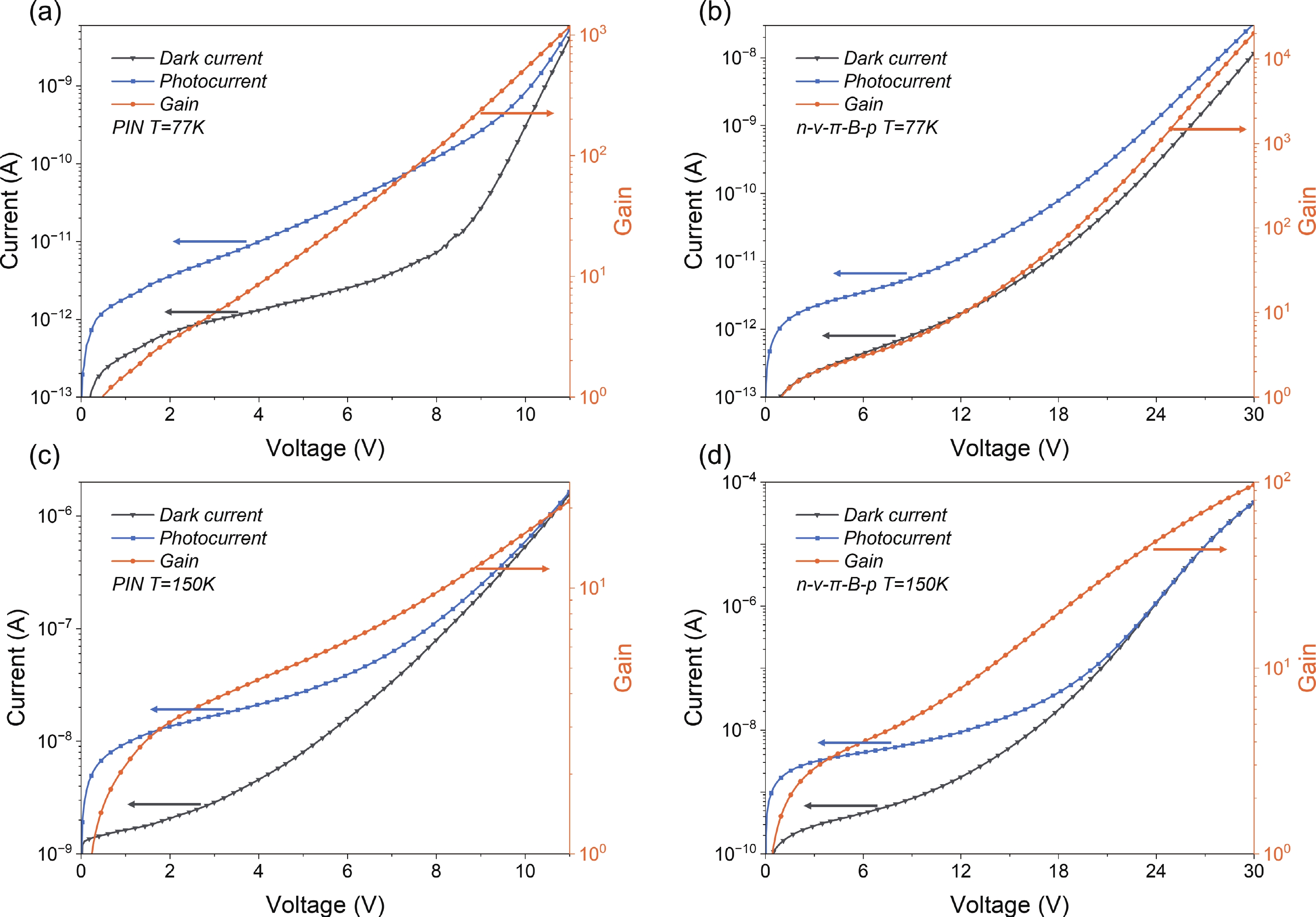
Abstract: HgCdTe avalanche photodiodes (APDs) are promising for mid-wave infrared weak-signal detection because electron-initiated avalanche multiplication can provide high gain with low excess noise. However, conventional PIN HgCdTe APDs still suffer from the trade-off between avalanche gain and dark current, especially under high reverse bias, where band-to-band tunneling and hot-carrier transport become significant. In this work, we combine experimental characterization and physics-based simulation to investigate this limitation. The temperature-dependent dark-current characteristics of reference PIN HgCdTe APDs are measured and reproduced using a calibrated device model incorporating recombination, tunneling, and avalanche processes. The agreement between experiment and simulation provides a reliable basis for analyzing dominant dark-current mechanisms and guiding device-structure optimization. Based on this experimentally calibrated framework, we propose a band-engineered n-v-π-B-p HgCdTe APD with redistributed electric field and an embedded barrier layer to suppress unfavorable carrier transport. Simulations predict that the proposed structure achieves higher gain at a given dark current than the conventional PIN design, with gains on the order of 104 at 77 K and 102 at 150 K. These results suggest that experimentally grounded band and field engineering is a promising route toward weak-signal MWIR signal detection.

Keywords: n-v-π-B-p HgCdTe avalanche photodetectorweak-signal detectionmid-wavelength infraredhigh gainlow dark current


[1]
Hadfield R H. Single-photon detectors for optical quantum information applications. Nat Photonics, 2009, 3(12): 696 doi: 10.1038/nphoton.2009.230
[2]
Cova S, Ghioni M, Lacaita A, et al. Avalanche photodiodes and quenching circuits for single-photon detection. Appl Opt, 1996, 35(12): 1956 doi: 10.1364/AO.35.001956
[3]
Martyniuk P, Wang P, Rogalski A, et al. Infrared avalanche photodiodes from bulk to 2D materials. Light Sci Appl, 2023, 12: 212 doi: 10.1038/s41377-023-01259-3
[4]
Kinch M A, Beck J D, Wan C F, et al. HgCdTe electron avalanche photodiodes. J Electron Mater, 2004, 33(6): 630 doi: 10.1007/s11664-004-0058-1
[5]
Beck J D, Wan C F, Kinch M A, et al. The HgCdTe electron avalanche photodiode. Infrared Detector Materials and Devices, Proc SPIE, 2004, 5564: 44 doi: 10.21236/ada081595
[6]
Singh A, Shukla A K, Pal R. HgCdTe e-avalanche photodiode detector arrays. AIP Adv, 2015, 5(8): 087172 doi: 10.1063/1.4929773
[7]
Sun X L, Abshire J B, Beck J D, et al. HgCdTe avalanche photodiode detectors for airborne and spaceborne lidar at infrared wavelengths. Opt Express, 2017, 25(14): 16589 doi: 10.1364/OE.25.016589
[8]
Rogalski A. HgCdTe infrared detector material: History, status and outlook. Rep Prog Phys, 2005, 68(10): 2267 doi: 10.1088/0034-4885/68/10/R01
[9]
Lei W, Antoszewski J, Faraone L. Progress, challenges, and opportunities for HgCdTe infrared materials and detectors. Appl Phys Rev, 2015, 2(4): 041303 doi: 10.1063/1.4936577
[10]
Sun X L, Abshire J B, Beck J D. HgCdTe e-APD detector arrays with single photon sensitivity for space lidar applications. Advanced Photon Counting Techniques VIII, Proc SPIE, 2014, 9114: 91140K doi: 10.1117/12.2053757
[11]
Sullivan W, Beck J, Scritchfield R, et al. Linear-mode HgCdTe avalanche photodiodes for photon-counting applications. J Electron Mater, 2015, 44(9): 3092 doi: 10.1007/s11664-015-3824-3
[12]
Rothman J, Pes S, Bleuet P, et al. Meso-photonic detection with HgCdTe APDs at high count rates. J Electron Mater, 2020, 49(11): 6881 doi: 10.1007/s11664-020-08461-8
[13]
Rothman J, Vojetta G, Moselle B, et al. Shockley–Haynes characterization of minority-carrier drift velocity, diffusion coefficient, and lifetime in HgCdTe avalanche photodiodes. J Electron Mater, 2010, 39(7): 837 doi: 10.1007/s11664-010-1247-8
[14]
Ferron A, Rothman J, Gravrand O. Modeling of dark current in HgCdTe infrared detectors. J Electron Mater, 2013, 42(11): 3303 doi: 10.1007/s11664-013-2733-6
[15]
Qiu W C, Hu W D, Chen L, et al. Dark current transport and avalanche mechanism in HgCdTe electron-avalanche photodiodes. IEEE Trans Electron Devices, 2015, 62(6): 1926 doi: 10.1109/TED.2015.2417193
[16]
Hu W D, Chen X S, Ye Z H, et al. Accurate simulation of temperature-dependent dark current in HgCdTe infrared detectors assisted by analytical modeling. J Electron Mater, 2010, 39(7): 981 doi: 10.1007/s11664-010-1121-8
[17]
Li Q, He J L, Hu W D, et al. Influencing sources for dark current transport and avalanche mechanisms in planar and mesa HgCdTe p-i-n electron-avalanche photodiodes. IEEE Trans Electron Devices, 2018, 65(2): 572 doi: 10.1109/TED.2017.2783352
[18]
Chen B C, Li Q, Chen J, et al. Mechanism of dark current dependence on reverse voltage in mid-wavelength infrared HgCdTe mesa PIN avalanche diode. Opt Quantum Electron, 2021, 53(1): 16 doi: 10.1007/s11082-020-02668-z
[19]
Arias J M, Pasko J G, Zandian M, et al. Planar p-on-n HgCdTe heterostructure photovoltaic detectors. Appl Phys Lett, 1993, 62(9): 976 doi: 10.1063/1.108538
[20]
Kopytko M, Rogalski A. HgCdTe barrier infrared detectors. Prog Quantum Electron, 2016, 47: 1 doi: 10.1109/drc.2012.6257026
[21]
Beattie A R, Landsberg P T. Auger effect in semiconductors. Proc R Soc Lond Ser A Math Phys Sci, 1959, 249(1256): 16 doi: 10.1088/0370-1301/68/5/108
[22]
van Roosbroeck W, Shockley W. Photon-radiative recombination of electrons and holes in germanium. Phys Rev, 1954, 94(6): 1558 doi: 10.1103/PhysRev.94.1558
[23]
Lopes V C, Syllaios A J, Chen M C. Minority carrier lifetime in mercury cadmium telluride. Semicond Sci Technol, 1993, 8(6S): 824 doi: 10.1088/0268-1242/8/6S/005
[24]
Nemirovsky Y, Fastow R, Meyassed M, et al. Trapping effects in HgCdTe. J Vac Sci Technol B Microelectron Nanometer Struct Process Meas Phenom, 1991, 9(3): 1829 doi: 10.1063/1.41060
[25]
Anderson W W. Tunnel current limitations of narrow bandgap infrared charge coupled devices. Infrared Phys, 1977, 17(2): 147 doi: 10.1016/0020-0891(77)90107-5
[26]
Okuto Y, Crowell C R. Threshold energy effect on avalanche breakdown voltage in semiconductor junctions. Solid State Electron, 1975, 18(2): 161 doi: 10.1016/0038-1101(75)90099-4
[27]
Chen J, Chen J, Li X, et al. High-performance HgCdTe avalanche photodetector enabled with suppression of band-to-band tunneling effect in mid-wavelength infrared. npj Quantum Mater, 2021, 6: 103 doi: 10.1038/s41535-021-00409-3
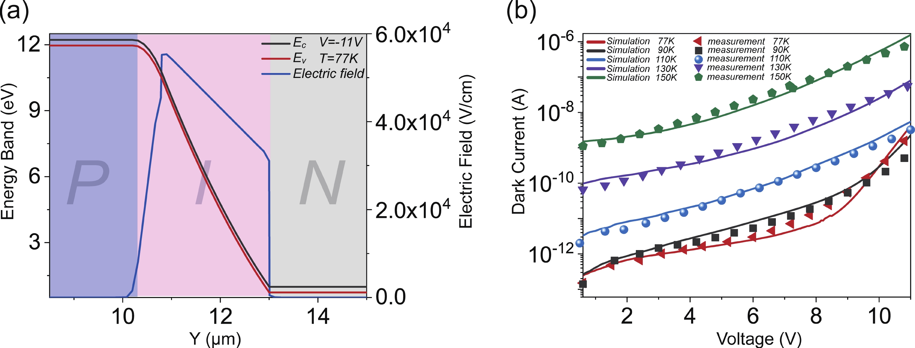
Fig. 1.  (Color online) Characterization of traditional PIN devices. (a) The configuration, energy band and electric field of PIN devices. (b) The measured and simulated dark current of PIN devices with various temperature. The solid lines and dots stand for simulated and measured results respectively.

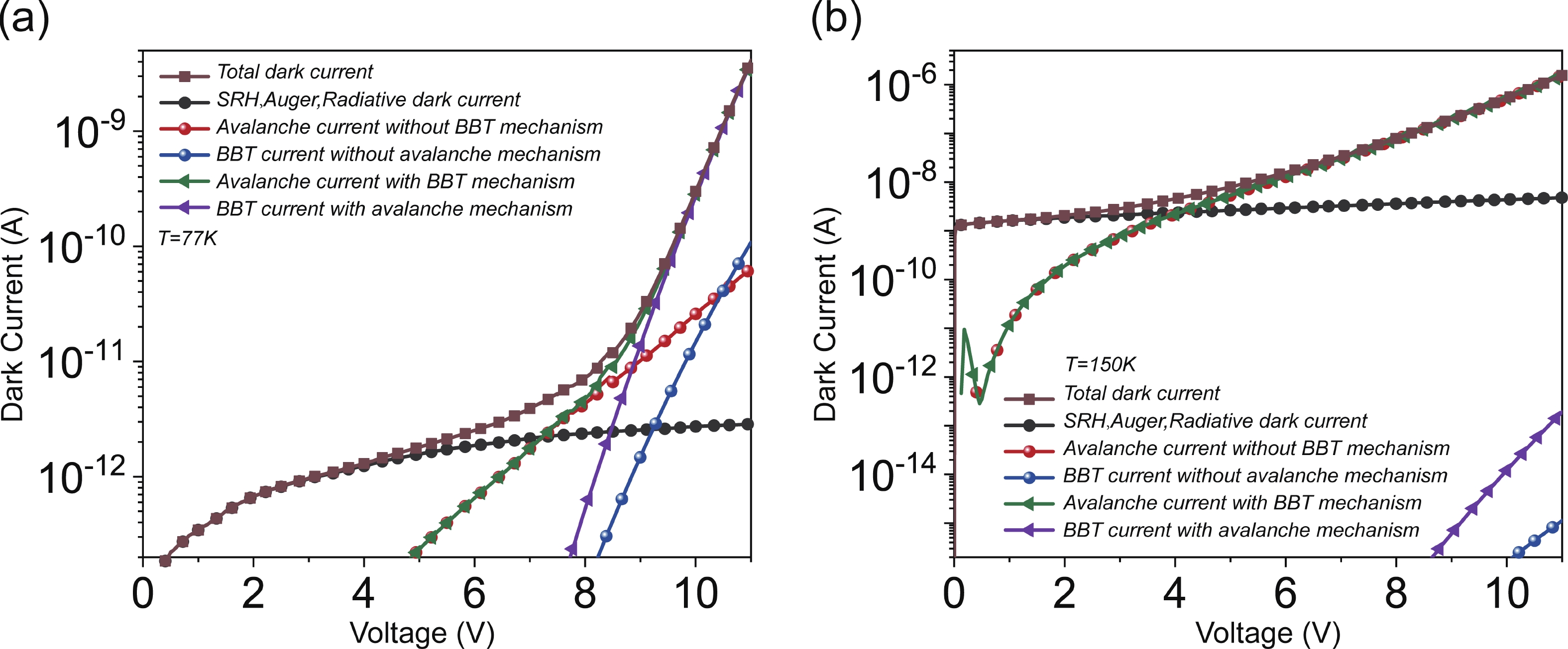
Fig. 2.  (Color online) Analysis of Dark current. (a) The dark current components at 77 K. (b) The dark current components at 150 K.

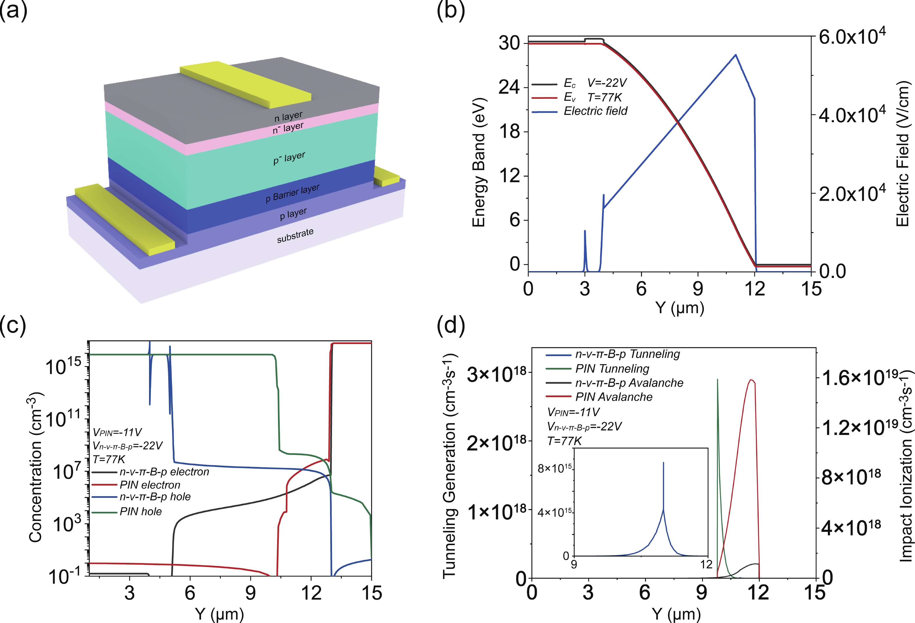
Fig. 3.  (Color online) n-v-π-B-p configuration and its comparison with PIN configuration. (a) The schematic of n-v-π-B-p configuration. (b) The energy band and electric field of n-v-π-B-p APD at high bias. (c) Carrier distributions of the n-v-π-B-p APD and PIN APD at 77 K. (The black curve represents the electron concentration. Since the electron concentration in the p-type region is extremely low, only the physically distinguishable range is displayed on the logarithmic axis to maintain the readability of the main carrier-distribution features.) (d) Comparison of BBT and avalanche generation rates between the n-v-π-B-p APD and PIN APD at 77 K. The inset presents a locally enlarged view of the selected region.

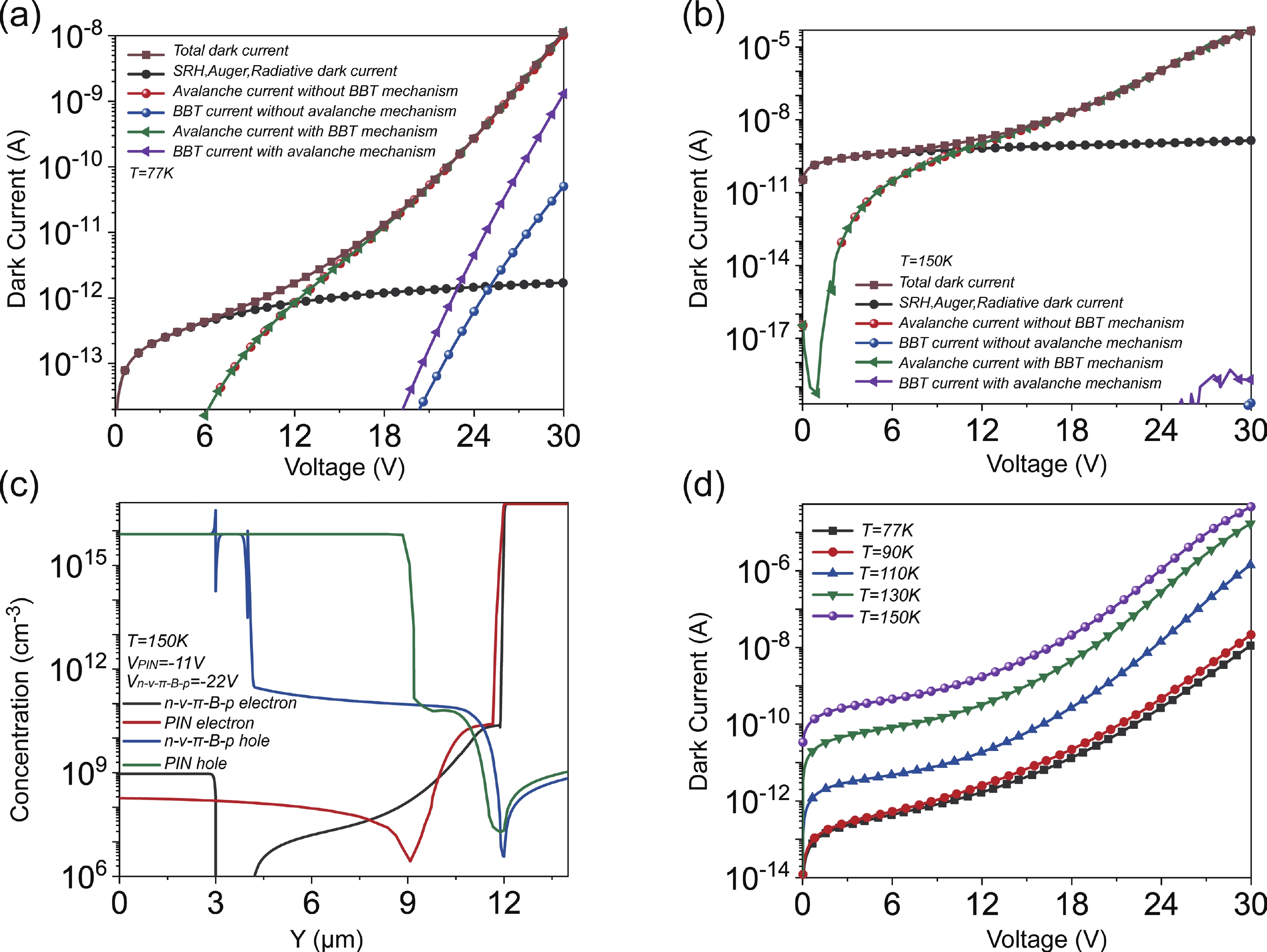
Fig. 4.  (Color online) Simulated analysis of n-v-π-B-p APD. (a) The dark current components of n-v-π-B-p APD at 77 K. (b) The dark current components of n-v-π-B-p APD at 150 K. (c) The hole and electron concentration of PIN APD at –11 V and n-v-π-B-p APD at –22 V at 150 K. (The black curve represents the electron concentration. Since the electron concentration in the p-type region is extremely low, only the physically distinguishable range is displayed on the logarithmic axis to maintain the readability of the main carrier-distribution features.) (d) The dark current curves with various temperature.

Fig. 5.  (Color online) Comparison of performance between the PIN APD and the n-v-π-B-p APD. (a) Dark current, photocurrent, and gain of the PIN APD at 77 K. (b) Dark current, photocurrent, and gain of the n-v-π-B-p APD at 77 K. (c) Dark current, photocurrent, and gain of the PIN APD at 150 K. (d) Dark current, photocurrent, and gain of the n-v-π-B-p APD at 150 K.

Table 1.   Key material and physical parameters used in the HgCdTe TCAD simulation.

ParameterExpression or valueUnit
Relative permittivity$ {\varepsilon }_{\text{r}}\text{=20.5-15.6x+5.7}{\text{x}}^{2} $N/A
Band gap$ {E}_{\text{g}}\text{=-0.302+1.93x-0.810}{\text{x}}^{2}+0.832{\text{x}}^{3}+5.35{\text{e}}^{-4}\text{(1-2x)T} $eV
Electron affinity$ \text{χ=4.23-0.813(}{E}_{\text{g}}-0.083) $eV
Electron effective mass$ m_{\text{e}}^{*}=1/(-0.6+6.333(2/{E}_{\text{g}}+1/({E}_{\text{g}}+1)) $N/A
Hole effective mass$ m_{\text{h}}^{*}=0.55 $N/A
Electron mobility$ {\mu }_{\text{e}}=9\times{10}^{4}{\text{(0.2/x)}}^{7.5}{\text{T}}^{-2{{\text{(0.2/x)}}^{0.6}}} $cm2/(V·s)
Hole mobility$ {\mu }_{\text{h}}=0.01{\mu }_{\text{e}} $cm2/(V·s)
Impact ionization modelOkuto–Crowell model[26]
DownLoad: CSV

Table 2.   The parameters of PIN and n-v-π-B-p configuration in simulation.

Device typeRegionThickness(μm)Doping concentration(cm-3)Cd component
PINp layer78e150.3033
n- layer21e150.3033
n layer26e160.3033
n-v-π-B-pp layer38e150.33
p Barrier layer18e150.41 − 0.57
p- π layer71e150.3033
n- v layer11e150.33
n layer36e160.33
DownLoad: CSV
[1]
Hadfield R H. Single-photon detectors for optical quantum information applications. Nat Photonics, 2009, 3(12): 696 doi: 10.1038/nphoton.2009.230
[2]
Cova S, Ghioni M, Lacaita A, et al. Avalanche photodiodes and quenching circuits for single-photon detection. Appl Opt, 1996, 35(12): 1956 doi: 10.1364/AO.35.001956
[3]
Martyniuk P, Wang P, Rogalski A, et al. Infrared avalanche photodiodes from bulk to 2D materials. Light Sci Appl, 2023, 12: 212 doi: 10.1038/s41377-023-01259-3
[4]
Kinch M A, Beck J D, Wan C F, et al. HgCdTe electron avalanche photodiodes. J Electron Mater, 2004, 33(6): 630 doi: 10.1007/s11664-004-0058-1
[5]
Beck J D, Wan C F, Kinch M A, et al. The HgCdTe electron avalanche photodiode. Infrared Detector Materials and Devices, Proc SPIE, 2004, 5564: 44 doi: 10.21236/ada081595
[6]
Singh A, Shukla A K, Pal R. HgCdTe e-avalanche photodiode detector arrays. AIP Adv, 2015, 5(8): 087172 doi: 10.1063/1.4929773
[7]
Sun X L, Abshire J B, Beck J D, et al. HgCdTe avalanche photodiode detectors for airborne and spaceborne lidar at infrared wavelengths. Opt Express, 2017, 25(14): 16589 doi: 10.1364/OE.25.016589
[8]
Rogalski A. HgCdTe infrared detector material: History, status and outlook. Rep Prog Phys, 2005, 68(10): 2267 doi: 10.1088/0034-4885/68/10/R01
[9]
Lei W, Antoszewski J, Faraone L. Progress, challenges, and opportunities for HgCdTe infrared materials and detectors. Appl Phys Rev, 2015, 2(4): 041303 doi: 10.1063/1.4936577
[10]
Sun X L, Abshire J B, Beck J D. HgCdTe e-APD detector arrays with single photon sensitivity for space lidar applications. Advanced Photon Counting Techniques VIII, Proc SPIE, 2014, 9114: 91140K doi: 10.1117/12.2053757
[11]
Sullivan W, Beck J, Scritchfield R, et al. Linear-mode HgCdTe avalanche photodiodes for photon-counting applications. J Electron Mater, 2015, 44(9): 3092 doi: 10.1007/s11664-015-3824-3
[12]
Rothman J, Pes S, Bleuet P, et al. Meso-photonic detection with HgCdTe APDs at high count rates. J Electron Mater, 2020, 49(11): 6881 doi: 10.1007/s11664-020-08461-8
[13]
Rothman J, Vojetta G, Moselle B, et al. Shockley–Haynes characterization of minority-carrier drift velocity, diffusion coefficient, and lifetime in HgCdTe avalanche photodiodes. J Electron Mater, 2010, 39(7): 837 doi: 10.1007/s11664-010-1247-8
[14]
Ferron A, Rothman J, Gravrand O. Modeling of dark current in HgCdTe infrared detectors. J Electron Mater, 2013, 42(11): 3303 doi: 10.1007/s11664-013-2733-6
[15]
Qiu W C, Hu W D, Chen L, et al. Dark current transport and avalanche mechanism in HgCdTe electron-avalanche photodiodes. IEEE Trans Electron Devices, 2015, 62(6): 1926 doi: 10.1109/TED.2015.2417193
[16]
Hu W D, Chen X S, Ye Z H, et al. Accurate simulation of temperature-dependent dark current in HgCdTe infrared detectors assisted by analytical modeling. J Electron Mater, 2010, 39(7): 981 doi: 10.1007/s11664-010-1121-8
[17]
Li Q, He J L, Hu W D, et al. Influencing sources for dark current transport and avalanche mechanisms in planar and mesa HgCdTe p-i-n electron-avalanche photodiodes. IEEE Trans Electron Devices, 2018, 65(2): 572 doi: 10.1109/TED.2017.2783352
[18]
Chen B C, Li Q, Chen J, et al. Mechanism of dark current dependence on reverse voltage in mid-wavelength infrared HgCdTe mesa PIN avalanche diode. Opt Quantum Electron, 2021, 53(1): 16 doi: 10.1007/s11082-020-02668-z
[19]
Arias J M, Pasko J G, Zandian M, et al. Planar p-on-n HgCdTe heterostructure photovoltaic detectors. Appl Phys Lett, 1993, 62(9): 976 doi: 10.1063/1.108538
[20]
Kopytko M, Rogalski A. HgCdTe barrier infrared detectors. Prog Quantum Electron, 2016, 47: 1 doi: 10.1109/drc.2012.6257026
[21]
Beattie A R, Landsberg P T. Auger effect in semiconductors. Proc R Soc Lond Ser A Math Phys Sci, 1959, 249(1256): 16 doi: 10.1088/0370-1301/68/5/108
[22]
van Roosbroeck W, Shockley W. Photon-radiative recombination of electrons and holes in germanium. Phys Rev, 1954, 94(6): 1558 doi: 10.1103/PhysRev.94.1558
[23]
Lopes V C, Syllaios A J, Chen M C. Minority carrier lifetime in mercury cadmium telluride. Semicond Sci Technol, 1993, 8(6S): 824 doi: 10.1088/0268-1242/8/6S/005
[24]
Nemirovsky Y, Fastow R, Meyassed M, et al. Trapping effects in HgCdTe. J Vac Sci Technol B Microelectron Nanometer Struct Process Meas Phenom, 1991, 9(3): 1829 doi: 10.1063/1.41060
[25]
Anderson W W. Tunnel current limitations of narrow bandgap infrared charge coupled devices. Infrared Phys, 1977, 17(2): 147 doi: 10.1016/0020-0891(77)90107-5
[26]
Okuto Y, Crowell C R. Threshold energy effect on avalanche breakdown voltage in semiconductor junctions. Solid State Electron, 1975, 18(2): 161 doi: 10.1016/0038-1101(75)90099-4
[27]
Chen J, Chen J, Li X, et al. High-performance HgCdTe avalanche photodetector enabled with suppression of band-to-band tunneling effect in mid-wavelength infrared. npj Quantum Mater, 2021, 6: 103 doi: 10.1038/s41535-021-00409-3
  • Search

    Advanced Search >>

    GET CITATION

    shu

    Export: BibTex EndNote

    Article Metrics

    Article views: 12 Times PDF downloads: 0 Times Cited by: 0 Times

    History

    Received: 28 April 2026 Revised: 01 July 2026 Online: Accepted Manuscript: 08 August 2026

    Catalog

      Email This Article

      User name:
      Email:*请输入正确邮箱
      Code:*验证码错误
      Juntong Liu, Jiahao Chen, Xin Li, Jin Chen, Feilong Yu, Guanhai Li, Xiaoshuang Chen, Wei Lu. n-v-π-B-p HgCdTe avalanche photodiodes for high gain and low dark current via band and field engineering[J]. Journal of Semiconductors, 2026, In Press. doi: 10.1088/1674-4926/26040047 ****J T Liu, J H Chen, X Li, J Chen, F L Yu, G H Li, X S Chen, and W Lu, n-v-π-B-p HgCdTe avalanche photodiodes for high gain and low dark current via band and field engineering[J]. J. Semicond., 2026, accepted doi: 10.1088/1674-4926/26040047
      Citation:
      Juntong Liu, Jiahao Chen, Xin Li, Jin Chen, Feilong Yu, Guanhai Li, Xiaoshuang Chen, Wei Lu. n-v-π-B-p HgCdTe avalanche photodiodes for high gain and low dark current via band and field engineering[J]. Journal of Semiconductors, 2026, In Press. doi: 10.1088/1674-4926/26040047 ****
      J T Liu, J H Chen, X Li, J Chen, F L Yu, G H Li, X S Chen, and W Lu, n-v-π-B-p HgCdTe avalanche photodiodes for high gain and low dark current via band and field engineering[J]. J. Semicond., 2026, accepted doi: 10.1088/1674-4926/26040047

      n-v-π-B-p HgCdTe avalanche photodiodes for high gain and low dark current via band and field engineering

      DOI: 10.1088/1674-4926/26040047
      CSTR: 32376.14.1674-4926.26040047
      More Information
      • Juntong Liu received his bachelor’s degree from Nanjing University of Information Science and Technology in 2021. He is currently pursuing his Ph.D. degree at the Shanghai Institute of Technical Physics, Chinese Academy of Sciences. His research interests include optoelectronic detection and microelectronic devices
      • Jiahao Chen is currently working toward the Ph.D. degree at the Shanghai Institute of Technical Physics, Chinese Academy of Sciences, Shanghai, China. His research interests include infrared optoelectronic devices, HgCdTe-based infrared detectors, and avalanche photodiodes. He has previously worked on silicon photodetectors with quantum-dot-based spectral response enhancement. His current research focuses on high-performance infrared detection and intelligent sensing technologies
      • Xin Li received his Ph.D. degree in physics from ShanghaiTech University in 2025. He is currently a postdoctoral researcher at the Shanghai Institute of Technical Physics, Chinese Academy of Sciences. His research interests include nonlinear photodetection, intelligent sensing, and mid-infrared avalanche photodetectors
      • Guanhai Li received the Ph.D. degree in optics from the University of Chinese Academy of Sciences, Beijing, China, in 2015. He is currently a Research Professor with the Shanghai Institute of Technology Physics, Chinese Academy of Sciences, Shanghai, China. His research interests include infrared single photon photodetectors, dielectric metasurface, and free-electron driven light source
      • Xiaoshuang Chen received the Ph.D. degree in condensed matter physics from Nanjing University, Nanjing, China, in 1995. He is currently a Full Professor with the Shanghai Institute of Technology Physics, Chinese Academy of Sciences, Shanghai, China. His research interests include infrared photo-electronic material design, high-speed electronic device design, and photonic crystal
      • Corresponding author: lixin21@mail.sitp.ac.cnghli0120@mail.sitp.ac.cnxschen@mail.sitp.ac.cn
      • Received Date: 2026-04-28
      • Revised Date: 2026-07-01
      • Available Online: 2026-08-08

      Catalog

        /

        DownLoad:  Full-Size Img  PowerPoint
        Return
        Return