


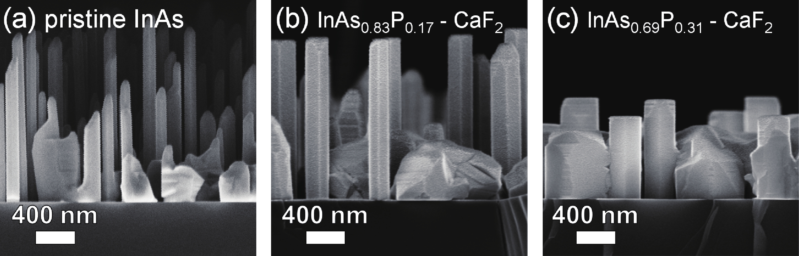
Fig. 1.
Cross-sectional SEM images of pristine InAs NWs (a), InAs0.83P0.17 / CaF2 NWs (b) and InAs0.69P0.31 / CaF2 NWs (c).
ARTICLES
Ratmir Ustimenko1, , Vladimir Fedorov1, 2, Danila Karaulov1, Maksim Vinnichenko1, Andrey Kaveev2, Demid Kirilenko3, Dmitry Miniv1, 2, Alexander Pavlov1, 2, David Hayrapetyan4, 5, Ivan Mukhin1, 2 and Dmitry Firsov1
Corresponding author: R. Ustimenko, Email: ratmirustimenko@yandex.ru
Abstract: Nanowires of narrow bandgap III–V semiconductors are very promising for efficient light-emitting and photosensitive devices operating in the mid-infrared spectrum range. Low-temperature infrared photoluminescence spectra of InAs and InAsP nanowires, including CaF2-passivated InAsP nanowires grown on a silicon substrate, were studied. The features in the spectra of InAsP nanowires were explained by the formation of a random close-packed stacking crystal structure with a predominance of the hexagonal (wurtzite) phase in nanowires and non-uniform distribution of stacking faults along their growth axis, as well as by radiation from parasitic bulk islands with the sphalerite phase. In structures without surface passivation, a red shift of spectrum was observed with increasing lattice temperature, consistent with the temperature dependence of the band gap. Passivation of the surface of InAsP nanowires using CaF2 leads to a nontrivial behavior of the spectral position of the photoluminescence intensity maximum due to a decrease in the contribution of surface states to nonradiative recombination at temperatures below 77 K. Moreover, it is shown that passivation allows to observe a photoluminescence signal at higher lattice temperatures compared to nonpassivated structures. The pump power dependence demonstrated a blue shift of the spectrum with increasing optical power, attributed to the band-filling effect (shift in the quasi-Fermi level)
Keywords: nanowires, passivation, defects in solid, photoluminescence, InAsP
| [1] |
Ren P Y, Hu W, Zhang Q L, et al. Band-selective infrared photodetectors with complete-composition-range InAsxP1-x alloy nanowires. Adv Mater, 2014, 26(44): 7444 doi: 10.1002/adma.201402945
|
| [2] |
Ju S, Facchetti A, Xuan Y, et al. Fabrication of fully transparent nanowire transistors for transparent and flexible electronics. Nat Nanotechnol., 2007, 2(6): 378 doi: 10.1038/nnano.2007.151
|
| [3] |
Pournia S, Linser S, Jnawali G, et al. Exploring the band structure of Wurtzite InAs nanowires using photocurrent spectroscopy. Nano Res, 2020, 13(6): 1586 doi: 10.1007/s12274-020-2774-0
|
| [4] |
Ghasemi M, Leshchenko E D, and Johansson J. Assembling your nanowire: an overview of composition tuning in ternary III–V nanowires. Nanotechnology, 2020, 32(7): 072001 doi: 10.1088/1361-6528/abc3e2
|
| [5] |
Fang Z M, Ma K Y, Jaw D H, et al. Photoluminescence of InSb, InAs, and InAsSb grown by organometallic vapor phase epitaxy. J Appl Phys, 1990, 67(11): 7034 doi: 10.1063/1.345050
|
| [6] |
Jurczak P, Zhang Y, Wu J, et al. Ten-fold enhancement of InAs nanowire photoluminescence emission with an InP passivation layer. Nano Lett, 2017, 17(6): 3629 doi: 10.1021/acs.nanolett.7b00803
|
| [7] |
Fedorov V, Vinnichenko M, Ustimenko R, et al. Non-uniformly strained core–shell InAs/InP nanowires for mid-infrared photonic applications. ACS Appl Nano Mater, 2023, 6(7): 5460 doi: 10.1021/acsanm.2c05575
|
| [8] |
De A, Pryor C E. Predicted band structures of III-V semiconductors in the wurtzite phase. Phys Rev B, 2010, 81(15): 155210 doi: 10.1103/PhysRevB.81.155210
|
| [9] |
Sourribes M J L, Isakov I, Panfilova M, et al. Mobility enhancement by Sb-mediated minimisation of stacking fault density in InAs nanowires grown on silicon. Nano Lett, 2014, 14(3): 1643 doi: 10.1021/nl5001554
|
| [10] |
Belabbes A, Panse C, Furthmüller J, et al. Electronic bands of III-V semiconductor polytypes and their alignment. Phys Rev B, 2012, 86(7): 075208 doi: 10.1103/PhysRevB.86.075208
|
| [11] |
Hiruma K, Yazawa M, Haraguchi K, et al. GaAs free-standing quantum-size wires. J Appl Phys, 1993, 74(5): 3162 doi: 10.1063/1.354585
|
| [12] |
Birman J L. Simplified LCAO method for zincblende, wurtzite, and mixed crystal structures. Phys Rev, 1959, 115(6): 1493 doi: 10.1103/PhysRev.115.1493
|
| [13] |
Yan Y, Dalpian G M, Al-Jassim M M, et al. Energetics and electronic structure of stacking faults in ZnO. Phys Rev B, 2004, 70(19): 193206 doi: 10.1103/PhysRevB.70.193206
|
| [14] |
Allen J E, Hemesath E R, Perea D E, et al. High-resolution detection of Au catalyst atoms in Si nanowires. Nat Nanotech, 2008, 3(3): 168 doi: 10.1038/nnano.2008.5
|
| [15] |
Anyebe E A. recent progress on the gold-free integration of ternary III–As antimonide nanowires directly on silicon. Nanomaterials, 2020, 10(10): 2064 doi: 10.3390/nano10102064
|
| [16] |
Kaveev A K, Fedorov V V, Pavlov A V, et al. Self-induced MBE-grown InAsP nanowires on Si wafers for SWIR applications. J Mater Chem C, 2025, 13(12): 6063 doi: 10.1039/D4TC04227A
|
| [17] |
Sun M H, Joyce H J, Gao Q, et al. Removal of surface states and recovery of band-edge emission in InAs nanowires through surface passivation. Nano Lett, 2012, 12(7): 3378 doi: 10.1021/nl300015w
|
| [18] |
Zanolli Z, Pistol M E, Fröberg L E, et al. Quantum-confinement effects in InAs–InP core–shell nanowires. J Phys Condens. Matter, 2007, 19(29): 295219 doi: 10.1088/0953-8984/19/29/295219
|
| [19] |
D F Bezuidenhout. Calcium Fluoride (CaF2). In Handbook of Optical Constants of Solids. Burlington: Academic Press, 1997: 815
|
| [20] |
Ishizaka A, Shiraki Y. Low temperature surface cleaning of silicon and its application to silicon MBE. J Electrochem Soc, 1986, 133(4): 666 doi: 10.1149/1.2108651
|
| [21] |
Al-Douri Y, Aourag H. The effect of pressure on the ionicity of In–V compounds. Phys B Condens Matter, 2002, 324(1): 173 doi: 10.1016/s0921-4526(02)01292-9
|
| [22] |
Cayron C. Diffraction artefacts from twins and stacking faults, and the mirage of hexagonal, polytypes or other superstructures. Scr Mater, 2021, 194: 113629 doi: 10.1016/j.scriptamat.2020.11.014
|
| [23] |
Gupta D, Goktas N I, Rao A, et al. Stacking defects in GaP nanowires: Electronic structure and optical properties. J Appl Phys, 2019, 126(8): 084306 doi: 10.1063/1.5110039
|
| [24] |
Möller M, de Lima M M, Cantarero A, et al. Optical emission of InAs nanowires. Nanotechnology, 2012, 23(37): 375704 doi: 10.1088/0957-4484/23/37/375704
|
| [25] |
Diedenhofen S L, Janssen O T A, Grzela G, et al. Strong geometrical dependence of the absorption of light in arrays of semiconductor nanowires. ACS Nano, 2011, 5(3): 2316 doi: 10.1021/nn103596n
|
| [26] |
Kaintz M, Cammarata A. From defects to devices: design guidelines for high-performance diamond-based solar cells and single-dopant diodes. 2026: arXiv: 2605.04942. https://arxiv.org/abs/2605.04942
|
| [27] |
Gonze X, Amadon B, Antonius G, et al. The Abinitproject: Impact, environment and recent developments. Comput Phys Commun, 2020, 248: 107042 doi: 10.1016/j.cpc.2019.107042
|
| [28] |
Tran F, Blaha P. Accurate band gaps of semiconductors and insulators with a semilocal exchange-correlation potential. Phys Rev Lett, 2009, 102(22): 226401 doi: 10.1103/PhysRevLett.102.226401
|
| [29] |
Vurgaftman I, Meyer J R, Ram-Mohan L R. Band parameters for III–V compound semiconductors and their alloys, J Appl Phys, 2001, 89(11): 5815
|
| [1] |
Ren P Y, Hu W, Zhang Q L, et al. Band-selective infrared photodetectors with complete-composition-range InAsxP1-x alloy nanowires. Adv Mater, 2014, 26(44): 7444 doi: 10.1002/adma.201402945
|
| [2] |
Ju S, Facchetti A, Xuan Y, et al. Fabrication of fully transparent nanowire transistors for transparent and flexible electronics. Nat Nanotechnol., 2007, 2(6): 378 doi: 10.1038/nnano.2007.151
|
| [3] |
Pournia S, Linser S, Jnawali G, et al. Exploring the band structure of Wurtzite InAs nanowires using photocurrent spectroscopy. Nano Res, 2020, 13(6): 1586 doi: 10.1007/s12274-020-2774-0
|
| [4] |
Ghasemi M, Leshchenko E D, and Johansson J. Assembling your nanowire: an overview of composition tuning in ternary III–V nanowires. Nanotechnology, 2020, 32(7): 072001 doi: 10.1088/1361-6528/abc3e2
|
| [5] |
Fang Z M, Ma K Y, Jaw D H, et al. Photoluminescence of InSb, InAs, and InAsSb grown by organometallic vapor phase epitaxy. J Appl Phys, 1990, 67(11): 7034 doi: 10.1063/1.345050
|
| [6] |
Jurczak P, Zhang Y, Wu J, et al. Ten-fold enhancement of InAs nanowire photoluminescence emission with an InP passivation layer. Nano Lett, 2017, 17(6): 3629 doi: 10.1021/acs.nanolett.7b00803
|
| [7] |
Fedorov V, Vinnichenko M, Ustimenko R, et al. Non-uniformly strained core–shell InAs/InP nanowires for mid-infrared photonic applications. ACS Appl Nano Mater, 2023, 6(7): 5460 doi: 10.1021/acsanm.2c05575
|
| [8] |
De A, Pryor C E. Predicted band structures of III-V semiconductors in the wurtzite phase. Phys Rev B, 2010, 81(15): 155210 doi: 10.1103/PhysRevB.81.155210
|
| [9] |
Sourribes M J L, Isakov I, Panfilova M, et al. Mobility enhancement by Sb-mediated minimisation of stacking fault density in InAs nanowires grown on silicon. Nano Lett, 2014, 14(3): 1643 doi: 10.1021/nl5001554
|
| [10] |
Belabbes A, Panse C, Furthmüller J, et al. Electronic bands of III-V semiconductor polytypes and their alignment. Phys Rev B, 2012, 86(7): 075208 doi: 10.1103/PhysRevB.86.075208
|
| [11] |
Hiruma K, Yazawa M, Haraguchi K, et al. GaAs free-standing quantum-size wires. J Appl Phys, 1993, 74(5): 3162 doi: 10.1063/1.354585
|
| [12] |
Birman J L. Simplified LCAO method for zincblende, wurtzite, and mixed crystal structures. Phys Rev, 1959, 115(6): 1493 doi: 10.1103/PhysRev.115.1493
|
| [13] |
Yan Y, Dalpian G M, Al-Jassim M M, et al. Energetics and electronic structure of stacking faults in ZnO. Phys Rev B, 2004, 70(19): 193206 doi: 10.1103/PhysRevB.70.193206
|
| [14] |
Allen J E, Hemesath E R, Perea D E, et al. High-resolution detection of Au catalyst atoms in Si nanowires. Nat Nanotech, 2008, 3(3): 168 doi: 10.1038/nnano.2008.5
|
| [15] |
Anyebe E A. recent progress on the gold-free integration of ternary III–As antimonide nanowires directly on silicon. Nanomaterials, 2020, 10(10): 2064 doi: 10.3390/nano10102064
|
| [16] |
Kaveev A K, Fedorov V V, Pavlov A V, et al. Self-induced MBE-grown InAsP nanowires on Si wafers for SWIR applications. J Mater Chem C, 2025, 13(12): 6063 doi: 10.1039/D4TC04227A
|
| [17] |
Sun M H, Joyce H J, Gao Q, et al. Removal of surface states and recovery of band-edge emission in InAs nanowires through surface passivation. Nano Lett, 2012, 12(7): 3378 doi: 10.1021/nl300015w
|
| [18] |
Zanolli Z, Pistol M E, Fröberg L E, et al. Quantum-confinement effects in InAs–InP core–shell nanowires. J Phys Condens. Matter, 2007, 19(29): 295219 doi: 10.1088/0953-8984/19/29/295219
|
| [19] |
D F Bezuidenhout. Calcium Fluoride (CaF2). In Handbook of Optical Constants of Solids. Burlington: Academic Press, 1997: 815
|
| [20] |
Ishizaka A, Shiraki Y. Low temperature surface cleaning of silicon and its application to silicon MBE. J Electrochem Soc, 1986, 133(4): 666 doi: 10.1149/1.2108651
|
| [21] |
Al-Douri Y, Aourag H. The effect of pressure on the ionicity of In–V compounds. Phys B Condens Matter, 2002, 324(1): 173 doi: 10.1016/s0921-4526(02)01292-9
|
| [22] |
Cayron C. Diffraction artefacts from twins and stacking faults, and the mirage of hexagonal, polytypes or other superstructures. Scr Mater, 2021, 194: 113629 doi: 10.1016/j.scriptamat.2020.11.014
|
| [23] |
Gupta D, Goktas N I, Rao A, et al. Stacking defects in GaP nanowires: Electronic structure and optical properties. J Appl Phys, 2019, 126(8): 084306 doi: 10.1063/1.5110039
|
| [24] |
Möller M, de Lima M M, Cantarero A, et al. Optical emission of InAs nanowires. Nanotechnology, 2012, 23(37): 375704 doi: 10.1088/0957-4484/23/37/375704
|
| [25] |
Diedenhofen S L, Janssen O T A, Grzela G, et al. Strong geometrical dependence of the absorption of light in arrays of semiconductor nanowires. ACS Nano, 2011, 5(3): 2316 doi: 10.1021/nn103596n
|
| [26] |
Kaintz M, Cammarata A. From defects to devices: design guidelines for high-performance diamond-based solar cells and single-dopant diodes. 2026: arXiv: 2605.04942. https://arxiv.org/abs/2605.04942
|
| [27] |
Gonze X, Amadon B, Antonius G, et al. The Abinitproject: Impact, environment and recent developments. Comput Phys Commun, 2020, 248: 107042 doi: 10.1016/j.cpc.2019.107042
|
| [28] |
Tran F, Blaha P. Accurate band gaps of semiconductors and insulators with a semilocal exchange-correlation potential. Phys Rev Lett, 2009, 102(22): 226401 doi: 10.1103/PhysRevLett.102.226401
|
| [29] |
Vurgaftman I, Meyer J R, Ram-Mohan L R. Band parameters for III–V compound semiconductors and their alloys, J Appl Phys, 2001, 89(11): 5815
|





Article views: 75 Times PDF downloads: 16 Times Cited by: 0 Times
Received: 28 April 2026 Revised: 09 July 2026 Online: Accepted Manuscript: 05 August 2026
| Citation: |
Ratmir Ustimenko, Vladimir Fedorov, Danila Karaulov, Maksim Vinnichenko, Andrey Kaveev, Demid Kirilenko, Dmitry Miniv, Alexander Pavlov, David Hayrapetyan, Ivan Mukhin, Dmitry Firsov. Low-temperature mid-infrared photoluminescence of InAsP nanowires[J]. Journal of Semiconductors, 2026, In Press. doi: 10.1088/1674-4926/26040048
****
R Ustimenko, V Fedorov, D Karaulov, M Vinnichenko, A Kaveev, D Kirilenko, D Miniv, A Pavlov, D Hayrapetyan, I Mukhin, and D Firsov, Low-temperature mid-infrared photoluminescence of InAsP nanowires[J]. J. Semicond., 2026, accepted doi: 10.1088/1674-4926/26040048

|
 Ratmir Ustimenko received his master's degree in 2021 from Peter the Great St. Petersburg Polytechnic University. He is currently a PhD student under the supervision of Prof. Dmitry Firsov. He is an employee of the scientific laboratories of "Optics of nonequilibrium electrons" and "Epitaxial nanostructures of A3B5 compounds on silicon". His research focused on infrared absorption and emission in GeSi quantum dots and InAs-based nanowires
 Maksim Vinnichenko received his PhD from St. Petersburg State Polytechnic University in Physics and Mathematics on the topic "Processes of recombination and heating of charge carriers in nanostructures with quantum wells" in 2013. He is currently an Associate Professor at Peter the Great St.Petersburg Polytechnic University, Russia. His research focuses on optical phenomena and nonequilibrium charge carriers in semiconductors and nanostructures
| [1] |
Ren P Y, Hu W, Zhang Q L, et al. Band-selective infrared photodetectors with complete-composition-range InAsxP1-x alloy nanowires. Adv Mater, 2014, 26(44): 7444 doi: 10.1002/adma.201402945
|
| [2] |
Ju S, Facchetti A, Xuan Y, et al. Fabrication of fully transparent nanowire transistors for transparent and flexible electronics. Nat Nanotechnol., 2007, 2(6): 378 doi: 10.1038/nnano.2007.151
|
| [3] |
Pournia S, Linser S, Jnawali G, et al. Exploring the band structure of Wurtzite InAs nanowires using photocurrent spectroscopy. Nano Res, 2020, 13(6): 1586 doi: 10.1007/s12274-020-2774-0
|
| [4] |
Ghasemi M, Leshchenko E D, and Johansson J. Assembling your nanowire: an overview of composition tuning in ternary III–V nanowires. Nanotechnology, 2020, 32(7): 072001 doi: 10.1088/1361-6528/abc3e2
|
| [5] |
Fang Z M, Ma K Y, Jaw D H, et al. Photoluminescence of InSb, InAs, and InAsSb grown by organometallic vapor phase epitaxy. J Appl Phys, 1990, 67(11): 7034 doi: 10.1063/1.345050
|
| [6] |
Jurczak P, Zhang Y, Wu J, et al. Ten-fold enhancement of InAs nanowire photoluminescence emission with an InP passivation layer. Nano Lett, 2017, 17(6): 3629 doi: 10.1021/acs.nanolett.7b00803
|
| [7] |
Fedorov V, Vinnichenko M, Ustimenko R, et al. Non-uniformly strained core–shell InAs/InP nanowires for mid-infrared photonic applications. ACS Appl Nano Mater, 2023, 6(7): 5460 doi: 10.1021/acsanm.2c05575
|
| [8] |
De A, Pryor C E. Predicted band structures of III-V semiconductors in the wurtzite phase. Phys Rev B, 2010, 81(15): 155210 doi: 10.1103/PhysRevB.81.155210
|
| [9] |
Sourribes M J L, Isakov I, Panfilova M, et al. Mobility enhancement by Sb-mediated minimisation of stacking fault density in InAs nanowires grown on silicon. Nano Lett, 2014, 14(3): 1643 doi: 10.1021/nl5001554
|
| [10] |
Belabbes A, Panse C, Furthmüller J, et al. Electronic bands of III-V semiconductor polytypes and their alignment. Phys Rev B, 2012, 86(7): 075208 doi: 10.1103/PhysRevB.86.075208
|
| [11] |
Hiruma K, Yazawa M, Haraguchi K, et al. GaAs free-standing quantum-size wires. J Appl Phys, 1993, 74(5): 3162 doi: 10.1063/1.354585
|
| [12] |
Birman J L. Simplified LCAO method for zincblende, wurtzite, and mixed crystal structures. Phys Rev, 1959, 115(6): 1493 doi: 10.1103/PhysRev.115.1493
|
| [13] |
Yan Y, Dalpian G M, Al-Jassim M M, et al. Energetics and electronic structure of stacking faults in ZnO. Phys Rev B, 2004, 70(19): 193206 doi: 10.1103/PhysRevB.70.193206
|
| [14] |
Allen J E, Hemesath E R, Perea D E, et al. High-resolution detection of Au catalyst atoms in Si nanowires. Nat Nanotech, 2008, 3(3): 168 doi: 10.1038/nnano.2008.5
|
| [15] |
Anyebe E A. recent progress on the gold-free integration of ternary III–As antimonide nanowires directly on silicon. Nanomaterials, 2020, 10(10): 2064 doi: 10.3390/nano10102064
|
| [16] |
Kaveev A K, Fedorov V V, Pavlov A V, et al. Self-induced MBE-grown InAsP nanowires on Si wafers for SWIR applications. J Mater Chem C, 2025, 13(12): 6063 doi: 10.1039/D4TC04227A
|
| [17] |
Sun M H, Joyce H J, Gao Q, et al. Removal of surface states and recovery of band-edge emission in InAs nanowires through surface passivation. Nano Lett, 2012, 12(7): 3378 doi: 10.1021/nl300015w
|
| [18] |
Zanolli Z, Pistol M E, Fröberg L E, et al. Quantum-confinement effects in InAs–InP core–shell nanowires. J Phys Condens. Matter, 2007, 19(29): 295219 doi: 10.1088/0953-8984/19/29/295219
|
| [19] |
D F Bezuidenhout. Calcium Fluoride (CaF2). In Handbook of Optical Constants of Solids. Burlington: Academic Press, 1997: 815
|
| [20] |
Ishizaka A, Shiraki Y. Low temperature surface cleaning of silicon and its application to silicon MBE. J Electrochem Soc, 1986, 133(4): 666 doi: 10.1149/1.2108651
|
| [21] |
Al-Douri Y, Aourag H. The effect of pressure on the ionicity of In–V compounds. Phys B Condens Matter, 2002, 324(1): 173 doi: 10.1016/s0921-4526(02)01292-9
|
| [22] |
Cayron C. Diffraction artefacts from twins and stacking faults, and the mirage of hexagonal, polytypes or other superstructures. Scr Mater, 2021, 194: 113629 doi: 10.1016/j.scriptamat.2020.11.014
|
| [23] |
Gupta D, Goktas N I, Rao A, et al. Stacking defects in GaP nanowires: Electronic structure and optical properties. J Appl Phys, 2019, 126(8): 084306 doi: 10.1063/1.5110039
|
| [24] |
Möller M, de Lima M M, Cantarero A, et al. Optical emission of InAs nanowires. Nanotechnology, 2012, 23(37): 375704 doi: 10.1088/0957-4484/23/37/375704
|
| [25] |
Diedenhofen S L, Janssen O T A, Grzela G, et al. Strong geometrical dependence of the absorption of light in arrays of semiconductor nanowires. ACS Nano, 2011, 5(3): 2316 doi: 10.1021/nn103596n
|
| [26] |
Kaintz M, Cammarata A. From defects to devices: design guidelines for high-performance diamond-based solar cells and single-dopant diodes. 2026: arXiv: 2605.04942. https://arxiv.org/abs/2605.04942
|
| [27] |
Gonze X, Amadon B, Antonius G, et al. The Abinitproject: Impact, environment and recent developments. Comput Phys Commun, 2020, 248: 107042 doi: 10.1016/j.cpc.2019.107042
|
| [28] |
Tran F, Blaha P. Accurate band gaps of semiconductors and insulators with a semilocal exchange-correlation potential. Phys Rev Lett, 2009, 102(22): 226401 doi: 10.1103/PhysRevLett.102.226401
|
| [29] |
Vurgaftman I, Meyer J R, Ram-Mohan L R. Band parameters for III–V compound semiconductors and their alloys, J Appl Phys, 2001, 89(11): 5815
|

 WeChat ID
Journal of Semiconductors © 2017 All Rights Reserved 京ICP备05085259号-2

 DownLoad:

