


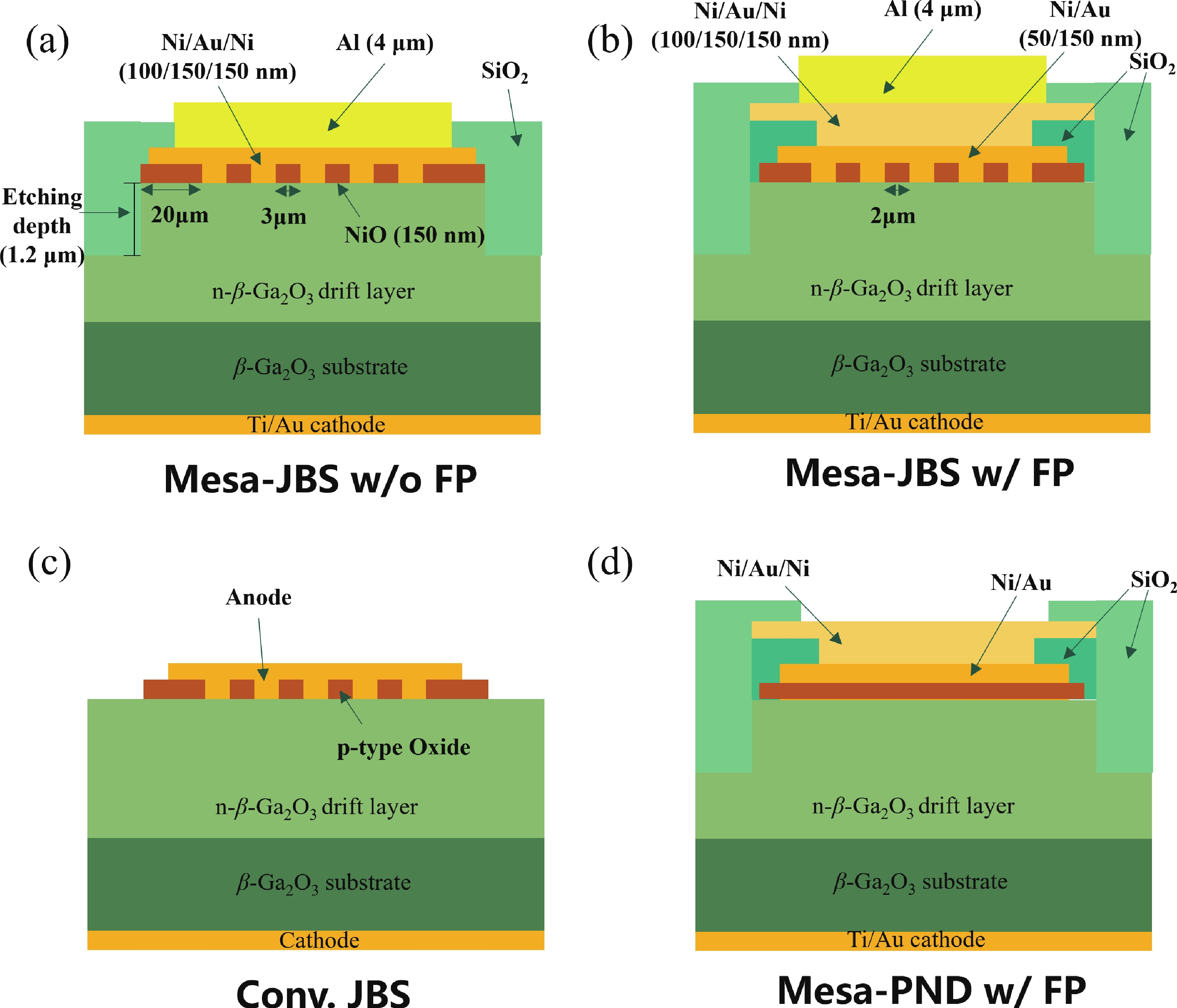
Fig. 1.
(Color online) Cross-sectional schematics of (a) the proposed β-Ga2O3 Mesa-JBS diode without, (b) with field plate, (c) conventional JBS, and (d) Mesa-PND with field plate.
ARTICLES
Shengliang Cheng1, Xing Lu1, , Shiyu Zhang1, Yiming Zhang1, Paiwen Fang1, Mingxian Luo1, Huichao Hu1, Rui Zhou1, Rui Xie1, Haowen Luo2, Huaxing Jiang2, Zhisheng Wu1, Jun Liang3, Zimin Chen1, Gang Wang1 and Yanli Pei1,
Corresponding author: Xing Lu, lux86@mail.sysu.edu.cn; Yanli Pei, peiyanli@mail.sysu.edu.cn
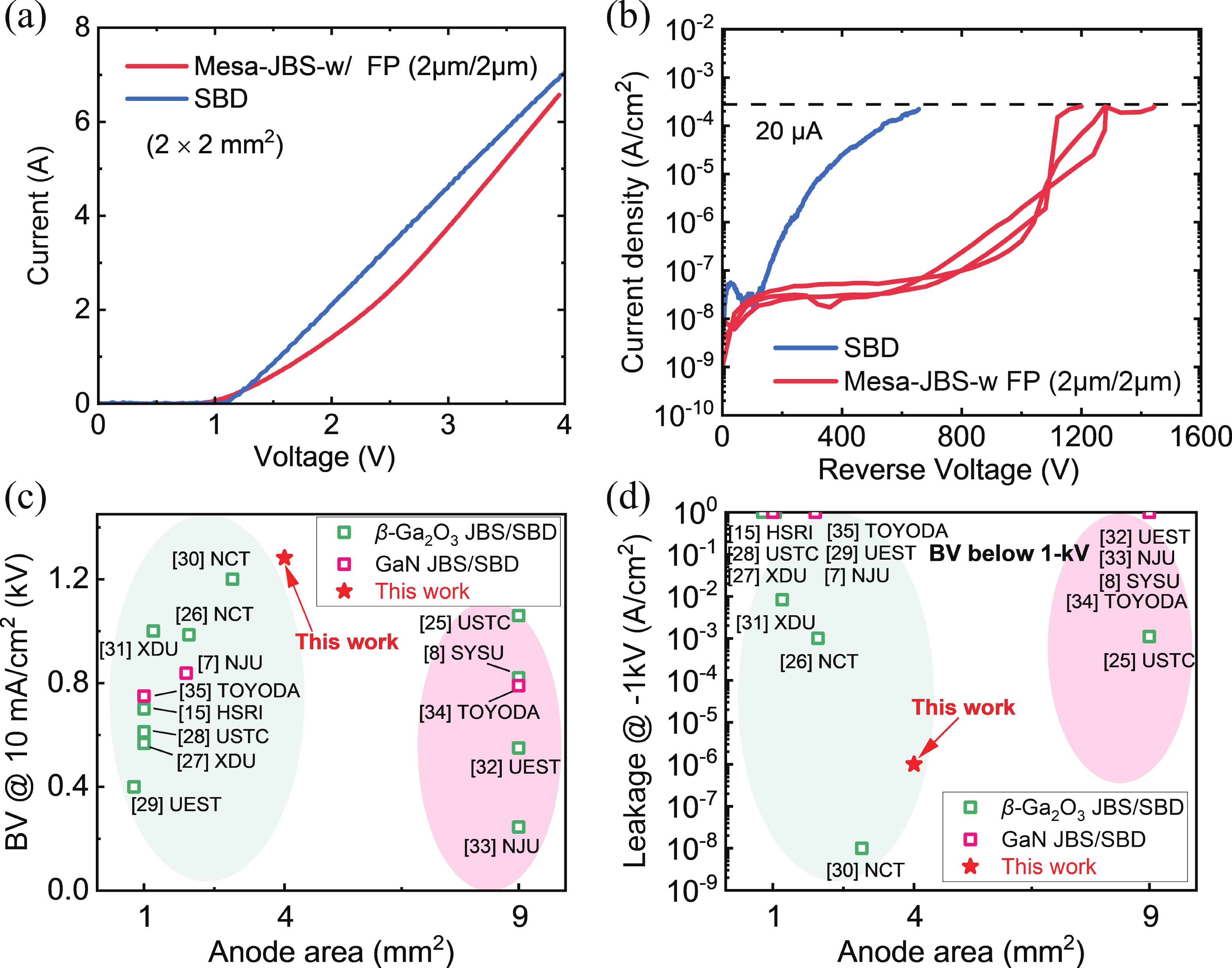
Abstract: This work reports deep-mesa-terminated β-Ga2O3 junction barrier Schottky (Mesa-JBS) diodes that achieve high breakdown voltage (BV) and ultralow reverse leakage current. The proposed architecture integrates a micron-scale deep mesa termination to suppress edge-induced leakage current with a buried p-NiO heterojunction beneath the anode to electrostatically suppress Schottky barrier tunneling, thereby mitigating both edge-related and Schottky-barrier tunneling leakage pathways. Small-area devices (0.2 × 0.2 mm2) exhibit a BV of 1.96 kV with a reverse leakage current density below 10–5 A/cm2 at 1 kV. To demonstrate scalability, large-area Mesa-JBS diodes (2 × 2 mm2) were fabricated and packaged for high-current operation. These devices deliver a forward current of 3.8 A at 3 V while sustaining a BV of up to 1.2 kV, with reverse leakage currents below 20 nA (approximately 1×10⁻⁶ A/cm2) at 1 kV. These results establish deep-mesa-terminated JBS diodes as a promising and scalable solution for high-voltage, low-loss β-Ga2O3 power rectifiers.
Keywords: β-Ga2O3, mesa-termination junction barrier Schottky (Mesa-JBS) diodes, large area devices, power device, low reverse leakage
| [1] |
Lu X, Deng Y X, Pei Y L, et al. Recent advances in NiO/Ga2O3 heterojunctions for power electronics. J Semicond, 2023, 44(6): 061802 doi: 10.1088/1674-4926/44/6/061802
|
| [2] |
Zhang M L, Liu Z, Yang L L, et al. β-Ga2O3-based power devices: A concise review. Crystals, 2022, 12(3): 406 doi: 10.3390/cryst12030406
|
| [3] |
Wang C L, Zhang J C, Xu S R, et al. Progress in state-of-the-art technologies of Ga2O3 devices. J Phys D Appl Phys, 2021, 54(24): 243001 doi: 10.1088/1361-6463/abe158
|
| [4] |
Pan A L, Wang Y Z, Zheng X F, et al. Insight into the leakage current transport mechanism transformation in β-Ga2O3 SBDs under forward bias stress. IEEE Trans Electron Devices, 2023, 70(6): 3185 doi: 10.1109/TED.2023.3267756
|
| [5] |
Neudeck P G. Silicon carbide technology. The VLSI Handbook. Boca Raton: CRC Press, 2007
|
| [6] |
Nakamura T, Nakano Y, Aketa M, et al. High performance SiC trench devices with ultra-low Ron. International Electron Devices Meeting (IEDM), 2012: 26.5. 1
|
| [7] |
Zhou F, Xu W Z, Ren F F, et al. Demonstration of avalanche and surge current robustness in GaN junction barrier Schottky diode with 600-V/10-A switching capability. IEEE Trans Power Electron, 2021, 36(11): 12163 doi: 10.1109/TPEL.2021.3076694
|
| [8] |
Cheng S L, Lai Y R, Lu X, et al. Low leakage current β-Ga2O3 self-aligned trench junction barrier Schottky diodes. IEEE Trans Electron Devices, 2025, 72(7): 3497 doi: 10.1109/TED.2025.3571880
|
| [9] |
Roy S, Bhattacharyya A, Ranga P, et al. High-k oxide field-plated vertical (001) β-Ga2O3 Schottky barrier diode with Baliga’s figure of merit over 1 GW/cm2. IEEE Electron Device Lett, 2021, 42(8): 1140 doi: 10.1109/LED.2021.3089945
|
| [10] |
Li W S, Nomoto K, Hu Z Y, et al. Field-plated Ga2O3 trench Schottky barrier diodes with a BV2/Ron, sp of up to 0.95 GW/cm2. IEEE Electron Device Lett, 2020, 41(1): 107 doi: 10.1109/LED.2019.2953559
|
| [11] |
Hao W B, Wu F H, Li W S, et al. Improved vertical β-Ga2O3 Schottky barrier diodes with conductivity-modulated p-NiO junction termination extension. IEEE Trans Electron Devices, 2023, 70(4): 2129 doi: 10.1109/TED.2023.3241885
|
| [12] |
Wang B Y, Xiao M, Spencer J, et al. 2.5 kV vertical Ga2O3 Schottky rectifier with graded junction termination extension. IEEE Electron Device Lett, 2023, 44(2): 221 doi: 10.1109/LED.2022.3229222
|
| [13] |
Han Z, Jian G Z, Zhou X Z, et al. 2.7 kV low leakage vertical PtOx/β-Ga2O3 Schottky barrier diodes with self-aligned mesa termination. IEEE Electron Device Lett, 2023, 44(10): 1680 doi: 10.1109/LED.2023.3305389
|
| [14] |
Dhara S, Kalarickal N K, Dheenan A, et al. β-Ga2O3 Schottky barrier diodes with 4.1 MV/cm field strength by deep plasma etching field-termination. Appl Phys Lett, 2022, 121(20): 203501 doi: 10.1063/5.0123284
|
| [15] |
Lv Y J, Wang Y G, Fu X C, et al. Demonstration of β-Ga2O3 junction barrier Schottky diodes with a Baliga’s figure of merit of 0.85 GW/cm2 or a 5 A/700 V handling capabilities. IEEE Trans Power Electron, 2021, 36(6): 6179 doi: 10.1109/TPEL.2020.3036442
|
| [16] |
Su C X, Zhou H, Zhang K, et al. Low turn-on voltage and 2.3 kV β-Ga2O3 heterojunction barrier Schottky diodes with Mo anode. Appl Phys Lett, 2024, 124(17): 173506 doi: 10.1063/5.0189890
|
| [17] |
Hao W B, Xu G W, Wu F H, et al. 2.7 kV β-Ga2O3 heterojunction barrier Schottky diode with low leakage current < 1 mA/cm2 based upon RESURF effect. International Symposium on Power Semiconductor Devices and ICs (ISPSD), 2024: 244
|
| [18] |
Hu T C, Wang Z P, Sun N, et al. A self-aligned Ga2O3 heterojunction barrier Schottky power diode. Appl Phys Lett, 2023, 123: 013507 doi: 10.1063/5.0147251
|
| [19] |
Yan Q L, Gong H H, Zhang J C, et al. β-Ga2O3 hetero-junction barrier Schottky diode with reverse leakage current modulation and BV2/Ron, sp value of 0.93 GW/cm2. Appl Phys Lett, 2021, 118(12): 122102. doi: 10.1063/5.0044130
|
| [20] |
He Q, Hao W B, Li Q Y, et al. β-Ga2O3 junction barrier Schottky diode with NiO p-well floating field rings. Chin Phys B, 2023, 32(12): 128507 doi: 10.1088/1674-1056/accf69
|
| [21] |
Gong H H, Yu X X, Xu Y, et al. β-Ga2O3 vertical heterojunction barrier Schottky diodes terminated with p-NiO field limiting rings. Appl Phys Lett, 2021, 118(20): 202102 doi: 10.1063/5.0050919
|
| [22] |
Gong H H, Sun N, Hu T C, et al. Ga2O3/NiO junction barrier Schottky diodes with ultra-low barrier TiN contact. Appl Phys Lett, 2024, 124(23): 233507 doi: 10.1063/5.0211124
|
| [23] |
Stein S R, Khachariya D, Mecouch W, et al. Analysis of vertical GaN JBS and p-n diodes by Mg ion implantation and ultrahigh-pressure annealing. IEEE Trans Electron Devices, 2024, 71(3): 1494 doi: 10.1109/TED.2023.3339592
|
| [24] |
Liu X K, Li B, Wu J Y, et al. Vertical GaN-on-GaN trench junction barrier Schottky diodes with a slanted sidewall. IEEE J Electron Devices Soc, 2024, 12: 34 doi: 10.1109/JEDS.2023.3340512
|
| [25] |
Wu F H, Wang Y G, Jian G Z, et al. Superior performance β-Ga2O3 junction barrier Schottky diodes implementing p-NiO heterojunction and beveled field plate for hybrid Cockcroft–Walton voltage multiplier. IEEE Trans Electron Devices, 2023, 70(3): 1199 doi: 10.1109/TED.2023.3239062
|
| [26] |
Takatsuka A, Miyamoto H, Sasaki K, et al. Fabrication of ampere-class p-Cu2O/n-β-Ga2O3 trench heterojunction barrier Schottky diodes and double-pulse evaluation. International Symposium on Power Semiconductor Devices and ICs (ISPSD), 2023: 342
|
| [27] |
Zhang F, Zheng X F, He Y L, et al. The impact of anode p+ islands layout on the performance of NiOx/β-Ga2O3 hetero-junction barrier Schottky diodes. IEEE Trans Electron Devices, 2023, 70(11): 5603 doi: 10.1109/TED.2023.3317815
|
| [28] |
Guo W, Han Z, Zhao X L, et al. Large-area β-Ga2O3 Schottky barrier diode and its application in DC–DC converters. J Semicond, 2023, 44(7): 072805 doi: 10.1088/1674-4926/44/7/072805
|
| [29] |
Wei Y X, Luo X R, Wang Y G, et al. Experimental study on static and dynamic characteristics of Ga2O3 Schottky barrier diodes with compound termination. IEEE Trans Power Electron, 2021, 36(10): 10976 doi: 10.1109/TPEL.2021.3069918
|
| [30] |
Otsuka F, Miyamoto H, Takatsuka A, et al. Large-size (1.7×1.7 mm2) β-Ga2O3 field-plated trench MOS-type Schottky barrier diodes with 1.2 kV breakdown voltage and 109 high on/off current ratio. Appl Phys Express, 2021, 15(1): 016501
|
| [31] |
Yan Q L, Gong H H, Zhou H, et al. Low density of interface trap states and temperature dependence study of Ga2O3 Schottky barrier diode with p-NiOx termination. Appl Phys Lett, 2022, 120(9): 092106. doi: 10.1063/5.0082377
|
| [32] |
Wei J, Wei Y X, Lu J, et al. Experimental study on electrical characteristics of large-size vertical β-Ga2O3 junction barrier Schottky diodes. International Symposium on Power Semiconductor Devices and ICs (ISPSD), 2022: 97
|
| [33] |
Gong H H, Zhou F, Xu W Z, et al. 1.37 kV/12 A NiO/β-Ga2O3 heterojunction diode with nanosecond reverse recovery and rugged surge-current capability. IEEE Trans Power Electron, 2021, 36(11): 12213 doi: 10.1109/TPEL.2021.3082640
|
| [34] |
Tanaka N, Hasegawa K, Yasunishi K, et al. 50 A vertical GaN Schottky barrier diode on a free-standing GaN substrate with blocking voltage of 790 V. Appl Phys Express, 2015, 8(7): 071001 doi: 10.7567/APEX.8.071001
|
| [35] |
Hasegawa K, Nishio G, Yasunishi K, et al. Vertical GaN trench MOS barrier Schottky rectifier maintaining low leakage current at 200 °C with blocking voltage of 750 V. Appl Phys Express, 2017, 10(12): 121002 doi: 10.7567/APEX.10.121002
|
| [1] |
Lu X, Deng Y X, Pei Y L, et al. Recent advances in NiO/Ga2O3 heterojunctions for power electronics. J Semicond, 2023, 44(6): 061802 doi: 10.1088/1674-4926/44/6/061802
|
| [2] |
Zhang M L, Liu Z, Yang L L, et al. β-Ga2O3-based power devices: A concise review. Crystals, 2022, 12(3): 406 doi: 10.3390/cryst12030406
|
| [3] |
Wang C L, Zhang J C, Xu S R, et al. Progress in state-of-the-art technologies of Ga2O3 devices. J Phys D Appl Phys, 2021, 54(24): 243001 doi: 10.1088/1361-6463/abe158
|
| [4] |
Pan A L, Wang Y Z, Zheng X F, et al. Insight into the leakage current transport mechanism transformation in β-Ga2O3 SBDs under forward bias stress. IEEE Trans Electron Devices, 2023, 70(6): 3185 doi: 10.1109/TED.2023.3267756
|
| [5] |
Neudeck P G. Silicon carbide technology. The VLSI Handbook. Boca Raton: CRC Press, 2007
|
| [6] |
Nakamura T, Nakano Y, Aketa M, et al. High performance SiC trench devices with ultra-low Ron. International Electron Devices Meeting (IEDM), 2012: 26.5. 1
|
| [7] |
Zhou F, Xu W Z, Ren F F, et al. Demonstration of avalanche and surge current robustness in GaN junction barrier Schottky diode with 600-V/10-A switching capability. IEEE Trans Power Electron, 2021, 36(11): 12163 doi: 10.1109/TPEL.2021.3076694
|
| [8] |
Cheng S L, Lai Y R, Lu X, et al. Low leakage current β-Ga2O3 self-aligned trench junction barrier Schottky diodes. IEEE Trans Electron Devices, 2025, 72(7): 3497 doi: 10.1109/TED.2025.3571880
|
| [9] |
Roy S, Bhattacharyya A, Ranga P, et al. High-k oxide field-plated vertical (001) β-Ga2O3 Schottky barrier diode with Baliga’s figure of merit over 1 GW/cm2. IEEE Electron Device Lett, 2021, 42(8): 1140 doi: 10.1109/LED.2021.3089945
|
| [10] |
Li W S, Nomoto K, Hu Z Y, et al. Field-plated Ga2O3 trench Schottky barrier diodes with a BV2/Ron, sp of up to 0.95 GW/cm2. IEEE Electron Device Lett, 2020, 41(1): 107 doi: 10.1109/LED.2019.2953559
|
| [11] |
Hao W B, Wu F H, Li W S, et al. Improved vertical β-Ga2O3 Schottky barrier diodes with conductivity-modulated p-NiO junction termination extension. IEEE Trans Electron Devices, 2023, 70(4): 2129 doi: 10.1109/TED.2023.3241885
|
| [12] |
Wang B Y, Xiao M, Spencer J, et al. 2.5 kV vertical Ga2O3 Schottky rectifier with graded junction termination extension. IEEE Electron Device Lett, 2023, 44(2): 221 doi: 10.1109/LED.2022.3229222
|
| [13] |
Han Z, Jian G Z, Zhou X Z, et al. 2.7 kV low leakage vertical PtOx/β-Ga2O3 Schottky barrier diodes with self-aligned mesa termination. IEEE Electron Device Lett, 2023, 44(10): 1680 doi: 10.1109/LED.2023.3305389
|
| [14] |
Dhara S, Kalarickal N K, Dheenan A, et al. β-Ga2O3 Schottky barrier diodes with 4.1 MV/cm field strength by deep plasma etching field-termination. Appl Phys Lett, 2022, 121(20): 203501 doi: 10.1063/5.0123284
|
| [15] |
Lv Y J, Wang Y G, Fu X C, et al. Demonstration of β-Ga2O3 junction barrier Schottky diodes with a Baliga’s figure of merit of 0.85 GW/cm2 or a 5 A/700 V handling capabilities. IEEE Trans Power Electron, 2021, 36(6): 6179 doi: 10.1109/TPEL.2020.3036442
|
| [16] |
Su C X, Zhou H, Zhang K, et al. Low turn-on voltage and 2.3 kV β-Ga2O3 heterojunction barrier Schottky diodes with Mo anode. Appl Phys Lett, 2024, 124(17): 173506 doi: 10.1063/5.0189890
|
| [17] |
Hao W B, Xu G W, Wu F H, et al. 2.7 kV β-Ga2O3 heterojunction barrier Schottky diode with low leakage current < 1 mA/cm2 based upon RESURF effect. International Symposium on Power Semiconductor Devices and ICs (ISPSD), 2024: 244
|
| [18] |
Hu T C, Wang Z P, Sun N, et al. A self-aligned Ga2O3 heterojunction barrier Schottky power diode. Appl Phys Lett, 2023, 123: 013507 doi: 10.1063/5.0147251
|
| [19] |
Yan Q L, Gong H H, Zhang J C, et al. β-Ga2O3 hetero-junction barrier Schottky diode with reverse leakage current modulation and BV2/Ron, sp value of 0.93 GW/cm2. Appl Phys Lett, 2021, 118(12): 122102. doi: 10.1063/5.0044130
|
| [20] |
He Q, Hao W B, Li Q Y, et al. β-Ga2O3 junction barrier Schottky diode with NiO p-well floating field rings. Chin Phys B, 2023, 32(12): 128507 doi: 10.1088/1674-1056/accf69
|
| [21] |
Gong H H, Yu X X, Xu Y, et al. β-Ga2O3 vertical heterojunction barrier Schottky diodes terminated with p-NiO field limiting rings. Appl Phys Lett, 2021, 118(20): 202102 doi: 10.1063/5.0050919
|
| [22] |
Gong H H, Sun N, Hu T C, et al. Ga2O3/NiO junction barrier Schottky diodes with ultra-low barrier TiN contact. Appl Phys Lett, 2024, 124(23): 233507 doi: 10.1063/5.0211124
|
| [23] |
Stein S R, Khachariya D, Mecouch W, et al. Analysis of vertical GaN JBS and p-n diodes by Mg ion implantation and ultrahigh-pressure annealing. IEEE Trans Electron Devices, 2024, 71(3): 1494 doi: 10.1109/TED.2023.3339592
|
| [24] |
Liu X K, Li B, Wu J Y, et al. Vertical GaN-on-GaN trench junction barrier Schottky diodes with a slanted sidewall. IEEE J Electron Devices Soc, 2024, 12: 34 doi: 10.1109/JEDS.2023.3340512
|
| [25] |
Wu F H, Wang Y G, Jian G Z, et al. Superior performance β-Ga2O3 junction barrier Schottky diodes implementing p-NiO heterojunction and beveled field plate for hybrid Cockcroft–Walton voltage multiplier. IEEE Trans Electron Devices, 2023, 70(3): 1199 doi: 10.1109/TED.2023.3239062
|
| [26] |
Takatsuka A, Miyamoto H, Sasaki K, et al. Fabrication of ampere-class p-Cu2O/n-β-Ga2O3 trench heterojunction barrier Schottky diodes and double-pulse evaluation. International Symposium on Power Semiconductor Devices and ICs (ISPSD), 2023: 342
|
| [27] |
Zhang F, Zheng X F, He Y L, et al. The impact of anode p+ islands layout on the performance of NiOx/β-Ga2O3 hetero-junction barrier Schottky diodes. IEEE Trans Electron Devices, 2023, 70(11): 5603 doi: 10.1109/TED.2023.3317815
|
| [28] |
Guo W, Han Z, Zhao X L, et al. Large-area β-Ga2O3 Schottky barrier diode and its application in DC–DC converters. J Semicond, 2023, 44(7): 072805 doi: 10.1088/1674-4926/44/7/072805
|
| [29] |
Wei Y X, Luo X R, Wang Y G, et al. Experimental study on static and dynamic characteristics of Ga2O3 Schottky barrier diodes with compound termination. IEEE Trans Power Electron, 2021, 36(10): 10976 doi: 10.1109/TPEL.2021.3069918
|
| [30] |
Otsuka F, Miyamoto H, Takatsuka A, et al. Large-size (1.7×1.7 mm2) β-Ga2O3 field-plated trench MOS-type Schottky barrier diodes with 1.2 kV breakdown voltage and 109 high on/off current ratio. Appl Phys Express, 2021, 15(1): 016501
|
| [31] |
Yan Q L, Gong H H, Zhou H, et al. Low density of interface trap states and temperature dependence study of Ga2O3 Schottky barrier diode with p-NiOx termination. Appl Phys Lett, 2022, 120(9): 092106. doi: 10.1063/5.0082377
|
| [32] |
Wei J, Wei Y X, Lu J, et al. Experimental study on electrical characteristics of large-size vertical β-Ga2O3 junction barrier Schottky diodes. International Symposium on Power Semiconductor Devices and ICs (ISPSD), 2022: 97
|
| [33] |
Gong H H, Zhou F, Xu W Z, et al. 1.37 kV/12 A NiO/β-Ga2O3 heterojunction diode with nanosecond reverse recovery and rugged surge-current capability. IEEE Trans Power Electron, 2021, 36(11): 12213 doi: 10.1109/TPEL.2021.3082640
|
| [34] |
Tanaka N, Hasegawa K, Yasunishi K, et al. 50 A vertical GaN Schottky barrier diode on a free-standing GaN substrate with blocking voltage of 790 V. Appl Phys Express, 2015, 8(7): 071001 doi: 10.7567/APEX.8.071001
|
| [35] |
Hasegawa K, Nishio G, Yasunishi K, et al. Vertical GaN trench MOS barrier Schottky rectifier maintaining low leakage current at 200 °C with blocking voltage of 750 V. Appl Phys Express, 2017, 10(12): 121002 doi: 10.7567/APEX.10.121002
|





Article views: 67 Times PDF downloads: 32 Times Cited by: 0 Times
Received: 07 May 2026 Revised: 29 June 2026 Online: Accepted Manuscript: 03 September 2026
| Citation: |
Shengliang Cheng, Xing Lu, Shiyu Zhang, Yiming Zhang, Paiwen Fang, Mingxian Luo, Huichao Hu, Rui Zhou, Rui Xie, Haowen Luo, Huaxing Jiang, Zhisheng Wu, Jun Liang, Zimin Chen, Gang Wang, Yanli Pei. Deep-mesa-terminated β-Ga2O3 Junction Barrier Schottky Diodes with Suppressed Reverse Leakage Current[J]. Journal of Semiconductors, 2026, In Press. doi: 10.1088/1674-4926/26050007
****
S L Cheng, X Lu, S Y Zhang, Y M Zhang, P W Fang, M X Luo, H C Hu, R Zhou, R Xie, H W Luo, H X Jiang, Z S Wu, J Liang, Z M Chen, G Wang, and Y L Pei, Deep-mesa-terminated β-Ga2O3 Junction Barrier Schottky Diodes with Suppressed Reverse Leakage Current[J]. J. Semicond., 2026, accepted doi: 10.1088/1674-4926/26050007

|
 Shengliang Cheng received the Ph.D. degree from the Sun Yat-sen University under the supervision of Prof. Yanli Pei and Prof. Xing Lu. His research focuses on Ga2O3 junction barrier Schottky diodes
 Xing Lu received the B.S. degree from Fudan University, Shanghai, China, and the Ph.D. degree from The Hong Kong Univer sity of Science and Technology, Hong Kong. He is currently an Professor with the State Key Laboratory of Optoelectronic Materials and Technologies, School of Elec tronics and Information Technology, Sun Yat-sen University, Guangzhou, China
 Jun Liang received his PhD from the Shanghai Institute of Microsystem and Information Technology, Chinese Academy of Sciences, in 2006. He is currently an Associate Professor at the School of Microelectronics, Shenzhen Institute of Information Technology. As early as 2018, Shenzhen Institute of Information Technology set up a project team to launch research on gallium oxide equipment, material epitaxy and device fabrication. The institute has undertaken national key research projects and industry collaborative projects, and built the Ministry of Education Collaborative Innovation Center for Compound Semiconductors
 Yanli Pei received the B.S. degree from Zhejiang University, Hangzhou, China, and the Ph.D. degree from the Hiroshima University, Japan. She is currently an Professor with the State Key Laboratory of Optoelectronic Materials and Technologies, School of Elec tronics and Information Technology, Sun Yat-sen University, Guangzhou, China
| [1] |
Lu X, Deng Y X, Pei Y L, et al. Recent advances in NiO/Ga2O3 heterojunctions for power electronics. J Semicond, 2023, 44(6): 061802 doi: 10.1088/1674-4926/44/6/061802
|
| [2] |
Zhang M L, Liu Z, Yang L L, et al. β-Ga2O3-based power devices: A concise review. Crystals, 2022, 12(3): 406 doi: 10.3390/cryst12030406
|
| [3] |
Wang C L, Zhang J C, Xu S R, et al. Progress in state-of-the-art technologies of Ga2O3 devices. J Phys D Appl Phys, 2021, 54(24): 243001 doi: 10.1088/1361-6463/abe158
|
| [4] |
Pan A L, Wang Y Z, Zheng X F, et al. Insight into the leakage current transport mechanism transformation in β-Ga2O3 SBDs under forward bias stress. IEEE Trans Electron Devices, 2023, 70(6): 3185 doi: 10.1109/TED.2023.3267756
|
| [5] |
Neudeck P G. Silicon carbide technology. The VLSI Handbook. Boca Raton: CRC Press, 2007
|
| [6] |
Nakamura T, Nakano Y, Aketa M, et al. High performance SiC trench devices with ultra-low Ron. International Electron Devices Meeting (IEDM), 2012: 26.5. 1
|
| [7] |
Zhou F, Xu W Z, Ren F F, et al. Demonstration of avalanche and surge current robustness in GaN junction barrier Schottky diode with 600-V/10-A switching capability. IEEE Trans Power Electron, 2021, 36(11): 12163 doi: 10.1109/TPEL.2021.3076694
|
| [8] |
Cheng S L, Lai Y R, Lu X, et al. Low leakage current β-Ga2O3 self-aligned trench junction barrier Schottky diodes. IEEE Trans Electron Devices, 2025, 72(7): 3497 doi: 10.1109/TED.2025.3571880
|
| [9] |
Roy S, Bhattacharyya A, Ranga P, et al. High-k oxide field-plated vertical (001) β-Ga2O3 Schottky barrier diode with Baliga’s figure of merit over 1 GW/cm2. IEEE Electron Device Lett, 2021, 42(8): 1140 doi: 10.1109/LED.2021.3089945
|
| [10] |
Li W S, Nomoto K, Hu Z Y, et al. Field-plated Ga2O3 trench Schottky barrier diodes with a BV2/Ron, sp of up to 0.95 GW/cm2. IEEE Electron Device Lett, 2020, 41(1): 107 doi: 10.1109/LED.2019.2953559
|
| [11] |
Hao W B, Wu F H, Li W S, et al. Improved vertical β-Ga2O3 Schottky barrier diodes with conductivity-modulated p-NiO junction termination extension. IEEE Trans Electron Devices, 2023, 70(4): 2129 doi: 10.1109/TED.2023.3241885
|
| [12] |
Wang B Y, Xiao M, Spencer J, et al. 2.5 kV vertical Ga2O3 Schottky rectifier with graded junction termination extension. IEEE Electron Device Lett, 2023, 44(2): 221 doi: 10.1109/LED.2022.3229222
|
| [13] |
Han Z, Jian G Z, Zhou X Z, et al. 2.7 kV low leakage vertical PtOx/β-Ga2O3 Schottky barrier diodes with self-aligned mesa termination. IEEE Electron Device Lett, 2023, 44(10): 1680 doi: 10.1109/LED.2023.3305389
|
| [14] |
Dhara S, Kalarickal N K, Dheenan A, et al. β-Ga2O3 Schottky barrier diodes with 4.1 MV/cm field strength by deep plasma etching field-termination. Appl Phys Lett, 2022, 121(20): 203501 doi: 10.1063/5.0123284
|
| [15] |
Lv Y J, Wang Y G, Fu X C, et al. Demonstration of β-Ga2O3 junction barrier Schottky diodes with a Baliga’s figure of merit of 0.85 GW/cm2 or a 5 A/700 V handling capabilities. IEEE Trans Power Electron, 2021, 36(6): 6179 doi: 10.1109/TPEL.2020.3036442
|
| [16] |
Su C X, Zhou H, Zhang K, et al. Low turn-on voltage and 2.3 kV β-Ga2O3 heterojunction barrier Schottky diodes with Mo anode. Appl Phys Lett, 2024, 124(17): 173506 doi: 10.1063/5.0189890
|
| [17] |
Hao W B, Xu G W, Wu F H, et al. 2.7 kV β-Ga2O3 heterojunction barrier Schottky diode with low leakage current < 1 mA/cm2 based upon RESURF effect. International Symposium on Power Semiconductor Devices and ICs (ISPSD), 2024: 244
|
| [18] |
Hu T C, Wang Z P, Sun N, et al. A self-aligned Ga2O3 heterojunction barrier Schottky power diode. Appl Phys Lett, 2023, 123: 013507 doi: 10.1063/5.0147251
|
| [19] |
Yan Q L, Gong H H, Zhang J C, et al. β-Ga2O3 hetero-junction barrier Schottky diode with reverse leakage current modulation and BV2/Ron, sp value of 0.93 GW/cm2. Appl Phys Lett, 2021, 118(12): 122102. doi: 10.1063/5.0044130
|
| [20] |
He Q, Hao W B, Li Q Y, et al. β-Ga2O3 junction barrier Schottky diode with NiO p-well floating field rings. Chin Phys B, 2023, 32(12): 128507 doi: 10.1088/1674-1056/accf69
|
| [21] |
Gong H H, Yu X X, Xu Y, et al. β-Ga2O3 vertical heterojunction barrier Schottky diodes terminated with p-NiO field limiting rings. Appl Phys Lett, 2021, 118(20): 202102 doi: 10.1063/5.0050919
|
| [22] |
Gong H H, Sun N, Hu T C, et al. Ga2O3/NiO junction barrier Schottky diodes with ultra-low barrier TiN contact. Appl Phys Lett, 2024, 124(23): 233507 doi: 10.1063/5.0211124
|
| [23] |
Stein S R, Khachariya D, Mecouch W, et al. Analysis of vertical GaN JBS and p-n diodes by Mg ion implantation and ultrahigh-pressure annealing. IEEE Trans Electron Devices, 2024, 71(3): 1494 doi: 10.1109/TED.2023.3339592
|
| [24] |
Liu X K, Li B, Wu J Y, et al. Vertical GaN-on-GaN trench junction barrier Schottky diodes with a slanted sidewall. IEEE J Electron Devices Soc, 2024, 12: 34 doi: 10.1109/JEDS.2023.3340512
|
| [25] |
Wu F H, Wang Y G, Jian G Z, et al. Superior performance β-Ga2O3 junction barrier Schottky diodes implementing p-NiO heterojunction and beveled field plate for hybrid Cockcroft–Walton voltage multiplier. IEEE Trans Electron Devices, 2023, 70(3): 1199 doi: 10.1109/TED.2023.3239062
|
| [26] |
Takatsuka A, Miyamoto H, Sasaki K, et al. Fabrication of ampere-class p-Cu2O/n-β-Ga2O3 trench heterojunction barrier Schottky diodes and double-pulse evaluation. International Symposium on Power Semiconductor Devices and ICs (ISPSD), 2023: 342
|
| [27] |
Zhang F, Zheng X F, He Y L, et al. The impact of anode p+ islands layout on the performance of NiOx/β-Ga2O3 hetero-junction barrier Schottky diodes. IEEE Trans Electron Devices, 2023, 70(11): 5603 doi: 10.1109/TED.2023.3317815
|
| [28] |
Guo W, Han Z, Zhao X L, et al. Large-area β-Ga2O3 Schottky barrier diode and its application in DC–DC converters. J Semicond, 2023, 44(7): 072805 doi: 10.1088/1674-4926/44/7/072805
|
| [29] |
Wei Y X, Luo X R, Wang Y G, et al. Experimental study on static and dynamic characteristics of Ga2O3 Schottky barrier diodes with compound termination. IEEE Trans Power Electron, 2021, 36(10): 10976 doi: 10.1109/TPEL.2021.3069918
|
| [30] |
Otsuka F, Miyamoto H, Takatsuka A, et al. Large-size (1.7×1.7 mm2) β-Ga2O3 field-plated trench MOS-type Schottky barrier diodes with 1.2 kV breakdown voltage and 109 high on/off current ratio. Appl Phys Express, 2021, 15(1): 016501
|
| [31] |
Yan Q L, Gong H H, Zhou H, et al. Low density of interface trap states and temperature dependence study of Ga2O3 Schottky barrier diode with p-NiOx termination. Appl Phys Lett, 2022, 120(9): 092106. doi: 10.1063/5.0082377
|
| [32] |
Wei J, Wei Y X, Lu J, et al. Experimental study on electrical characteristics of large-size vertical β-Ga2O3 junction barrier Schottky diodes. International Symposium on Power Semiconductor Devices and ICs (ISPSD), 2022: 97
|
| [33] |
Gong H H, Zhou F, Xu W Z, et al. 1.37 kV/12 A NiO/β-Ga2O3 heterojunction diode with nanosecond reverse recovery and rugged surge-current capability. IEEE Trans Power Electron, 2021, 36(11): 12213 doi: 10.1109/TPEL.2021.3082640
|
| [34] |
Tanaka N, Hasegawa K, Yasunishi K, et al. 50 A vertical GaN Schottky barrier diode on a free-standing GaN substrate with blocking voltage of 790 V. Appl Phys Express, 2015, 8(7): 071001 doi: 10.7567/APEX.8.071001
|
| [35] |
Hasegawa K, Nishio G, Yasunishi K, et al. Vertical GaN trench MOS barrier Schottky rectifier maintaining low leakage current at 200 °C with blocking voltage of 750 V. Appl Phys Express, 2017, 10(12): 121002 doi: 10.7567/APEX.10.121002
|

 WeChat ID
Journal of Semiconductors © 2017 All Rights Reserved 京ICP备05085259号-2

 DownLoad:

