J. Semicond. >  Just Accepted

ARTICLES

1.6 kV/ 1.47 GW·cm−2 AlGaN/GaN-based Schottky barrier diodes grown on Si substrate with n-GaN/p-NiO/n-GaN lateral junctions

Jingting He1, §, Zhizhong Wang2, §, Wenjie Mi1, Qiong Zhang1, Fuping Huang1, Chunshuang Chu1, Kangkai Tian1, Haoyan Liu3, Yonghui Zhang3, Shuting Cai1, Xiao Wei Sun4 and Zihui Zhang1, 3,

+ Author Affiliations

 Corresponding author: Zihui Zhang, zh.zhang@hebut.edu.cn

DOI: 10.1088/1674-4926/26050011CSTR: 32376.14.1674-4926.26050011

PDF

Turn off MathJax

Abstract: AlGaN/GaN-based Schottky barrier diodes grown on Si substrates with n-GaN/p-NiO/n-GaN lateral junctions are proposed and fabricated. The n-GaN/p-NiO/n-GaN lateral junctions effectively extend the depletion region in the GaN drift layer. The more homogenized electric field reduces the electric field magnitude near both the Schottky contact and the field plate (FP) edge. Consequently, the fabricated lateral power device achieves a breakdown voltage (BV) of ~1.6 kV and yields a high Baliga’s figure of merit (BFOM) of ~1.47 GW·cm−2. The n-GaN/p-NiO/n-GaN lateral junctions also contribute to suppressing the electron trapping effect and reducing the dynamic specific on-resistance (Ron,sp) by 1.5 times. With the developed physical models, we have also investigated the impact of different p-NiO designs on the blocking effect for the proposed device. We report that the n-GaN layer in the n-GaN/p-NiO/n-GaN lateral junctions shall be effectively depleted so that AlGaN/GaN-based Schottky barrier diodes with high BV can be achieved.

Keywords: AlGaN/GaN-based Schottky barrier diodespower device2DEG


[1]
Teo K H, Zhang Y H, Chowdhury N, et al. Emerging GaN technologies for power, RF, digital, and quantum computing applications: Recent advances and prospects. J Appl Phys, 2021, 130(16): 160902 doi: 10.1063/5.0061555
[2]
Buffolo M, Favero D, Marcuzzi A, et al. Review and outlook on GaN and SiC power devices: Industrial state-of-the-art, applications, and perspectives. IEEE Trans Electron Devices, 2024, 71(3): 1344 doi: 10.1109/TED.2023.3346369
[3]
Zhou Q, Jin Y, Shi Y Y, et al. High reverse blocking and low onset voltage AlGaN/GaN-on-Si lateral power diode with MIS-gated hybrid anode. IEEE Electron Device Lett, 2015, 36(7): 660 doi: 10.1109/LED.2015.2432171
[4]
Tao M, Wang M J, Wen C P, et al. Kilovolt GaN MOSHEMT on silicon substrate with breakdown electric field close to the theoretical limit. 2017 29th International Symposium on Power Semiconductor Devices and IC’s (ISPSD). Sapporo, Japan. IEEE, 2017: 93
[5]
Nela L, Yildirim H K, Erine C, et al. Conformal passivation of multi-channel GaN power transistors for reduced current collapse. IEEE Electron Device Lett, 2021, 42(1): 86 doi: 10.1109/LED.2020.3038808
[6]
Zhang T, Li R H, Lu J, et al. A 0.43 V/90 nA/mm lateral AlGaN/GaN Schottky barrier diode with plasma-free groove anode technique. IEEE Electron Device Lett, 2021, 42(12): 1747 doi: 10.1109/LED.2021.3123652
[7]
Wong M S, Lee C M, Myers D J, et al. Size-independent peak efficiency of III-nitride micro-light-emitting-diodes using chemical treatment and sidewall passivation. Appl Phys Express, 2019, 12(9): 097004 doi: 10.7567/1882-0786/ab3949
[8]
Wang H Y, Mao W, Yang C, et al. Lateral AlGaN/GaN Schottky barrier diode with arrayed p-GaN islands termination. IEEE Trans Electron Devices, 2021, 68(12): 6046 doi: 10.1109/TED.2021.3118326
[9]
Soni A, Amogh K M, Shrivastava M. Design guidelines and performance tradeoffs in recessed AlGaN/GaN Schottky barrier diodes. IEEE Trans Electron Devices, 2020, 67(11): 4834 doi: 10.1109/TED.2020.3024354
[10]
Lee H S, Kalarickal N K, Rahman M W, et al. High-permittivity dielectric edge termination for vertical high voltage devices. J Comput Electron, 2020, 19(4): 1538 doi: 10.1007/s10825-020-01553-y
[11]
Wang Z Z, Huang F P, Chu C S, et al. 2.5 kV/1.95 GW/cm2 AlGaN/GaN-based lateral Schottky barrier diodes with a high-k field plate to reduce reverse current. IEEE Trans Electron Devices, 2024, 71(6): 3811 doi: 10.1109/TED.2024.3388377
[12]
He J T, Wang Z Z, Huang F P, et al. Physical model development for fabricating MIS-anode-based 1100 V AlGaN/GaN-based lateral Schottky barrier diodes grown on silicon substrate with low leakage current. Adv Electron Mater, 2025, 11(13): 2500111 doi: 10.1002/aelm.202500111
[13]
Xu T, Tang Z Q, Zhou Z Y, et al. Simulation optimization of AlGaN/GaN SBD with field plate structures and recessed anode. Micromachines, 2023, 14(6): 1121 doi: 10.3390/mi14061121
[14]
Shi Y T, Ren F F, Xu W Z, et al. Realization of p-type gallium nitride by magnesium ion implantation for vertical power devices. Sci Rep, 2019, 9: 8796 doi: 10.1038/s41598-019-45177-0
[15]
Guo H, Gong H H, Shao P F, et al. Over 1200 V normally-OFF p-NiO gated AlGaN/GaN HEMTs on Si with a small threshold voltage shift. IEEE Electron Device Lett, 2022, 43(2): 268 doi: 10.1109/LED.2021.3137510
[16]
Qin Y, Xiao M, Zhang R Z, et al. 1 kV GaN-on-Si quasi-vertical Schottky rectifier. IEEE Electron Device Lett, 2023, 44(7): 1052 doi: 10.1109/LED.2023.3282025
[17]
Huang F P, Chu C S, Wang Z Z, et al. GaN-based quasi-vertical Schottky barrier diode hybridized with p-NiO layer to achieve 1.1 kV breakdown voltage and enhance the current spreading effect. Appl Phys Express, 2022, 15(8): 084001 doi: 10.35848/1882-0786/ac7eac
[18]
Khadar R A, Floriduz A, Wang T F, et al. P-NiO junction termination extensions for GaN power devices. Appl Phys Express, 2021, 14(7): 071006 doi: 10.35848/1882-0786/ac09ff
[19]
Li S C, Yang S, Han Z, et al. Vertical GaN Schottky barrier diode with hybrid P-NiO junction termination extension. IEEE J Electron Devices Soc, 2024, 12: 548 doi: 10.1109/JEDS.2024.3432783
[20]
Gong H H, Yu X X, Xu Y, et al. β-Ga2O3 vertical heterojunction barrier Schottky diodes terminated with p-NiO field limiting rings. Appl Phys Lett, 2021, 118(20): 202102 doi: 10.1063/5.0050919
[21]
Xiao M, Ma Y W, Du Z H, et al. First demonstration of vertical superjunction diode in GaN. 2022 International Electron Devices Meeting (IEDM). San Francisco, CA, USA. IEEE, 2022: 35.6. 1
[22]
Malik R R, Karthik S R, Joshi V, et al. Experimental validation of buffer traps-driven electric field dynamics governing breakdown and leakage trends in AlGaN/GaN heterostructures. 2025 IEEE International Reliability Physics Symposium (IRPS). Monterey, CA, USA. IEEE, 2025: P26. GaN
[23]
Wang Z Z, He J T, Huang F P, et al. AlGaN/GaN-based SBDs grown on silicon substrates with trenched n+-GaN cap layer and local passivation layer to improve BFOM and dynamic properties. J Semicond, 2025, 46(9): 092502 doi: 10.1088/1674-4926/25010024
[24]
Wang Z Z, Huang F P, Chu C S, et al. On the super-junction formed by using field plate for lateral AlGaN/GaN-based Schottky barrier diodes. Jpn J Appl Phys, 2023, 62(9): 094001 doi: 10.35848/1347-4065/acf17a
[25]
Rahman M W, Chandrasekar H, Razzak T, et al. Hybrid BaTiO3/SiNx/AlGaN/GaN lateral Schottky barrier diodes with low turn-on and high breakdown performance. Appl Phys Lett, 2021, 119: 013504 doi: 10.1063/5.0055946
[26]
Colón A, Douglas E A, Pope A J, et al. Demonstration of a 9 kV reverse breakdown and 59 mΩ-cm2 specific on-resistance AlGaN/GaN Schottky barrier diode. Solid State Electron, 2019, 151: 47 doi: 10.1016/j.sse.2018.10.009
[27]
Zhang T, Zhang Y N, Li R H, et al. Current transport mechanism of AlGaN-channel Schottky barrier diode with extremely low leakage current and high blocking voltage of 2.55 kV. Appl Phys Lett, 2022, 120(9): 092102 doi: 10.1063/5.0077691
[28]
Deng S, Liu K, Wang C, et al. The influence of recessed floating metal rings structure on electrical properties of AlGaN/GaN Schottky barrier diodes. Phys Status Solidi A, 2022, 219(2): 2100502 doi: 10.1002/pssa.202100502
[29]
Lei J C, Wei J, Tang G F, et al. 650-V double-channel lateral Schottky barrier diode with dual-recess gated anode. IEEE Electron Device Lett, 2018, 39(2): 260 doi: 10.1109/LED.2017.2783908
[30]
Zhu M D, Song B, Qi M, et al. 1.9-kV AlGaN/GaN lateral Schottky barrier diodes on silicon. IEEE Electron Device Lett, 2015, 36(4): 375 doi: 10.1109/LED.2015.2404309
[31]
Zhu L Y, Zhou Q, Yang X, et al. High-performance ultrathin-barrier AlGaN/GaN hybrid anode diode with Al2O3 gate dielectric and In situ Si3N4-cap passivation. IEEE Trans Electron Devices, 2020, 67(10): 4136 doi: 10.1109/TED.2020.3018416
[32]
Huang F P, Mi W J, He J T, et al. 1.06-kV polarization gate-assisted Si-based AlGaN/GaN Schottky barrier diode with 0.817-GW/cm2 BFOM and 10–5-A/cm2 Leakage current. IEEE Trans Electron Devices, 2025, 72(12): 6918 doi: 10.1109/TED.2025.3618521
[33]
Lee H S, Jung D Y, Park Y, et al. 0.34 VT AlGaN/GaN-on-Si large Schottky barrier diode with recessed dual anode metal. IEEE Electron Device Lett, 2015, 36(11): 1132 doi: 10.1109/LED.2015.2475178
[34]
Ha M W, Han M K, Hahn C K. Effects of post-oxidation on leakage current of high-voltage AlGaN/GaN Schottky barrier diodes on Si(111) substrates. Solid State Electron, 2013, 81: 1 doi: 10.1016/j.sse.2012.11.006
[35]
Chang T F, Huang C F, Yang T Y, et al. Low Turn-on voltage dual metal AlGaN/GaN Schottky barrier diode. Solid State Electron, 2015, 105: 12 doi: 10.1016/j.sse.2014.11.024
[36]
Chiu H C, Chen S C, Chiu J W, et al. AlGaN/GaN Schottky barrier diodes on silicon substrates with various Fe doping concentrations in the buffer layers. Microelectron Reliab, 2018, 83: 238 doi: 10.1016/j.microrel.2017.05.034
[37]
Lu Y, Zhou F, Xu W Z, et al. Multi-aperture anode based AlGaN/GaN Schottky barrier diodes with low turn-on voltage and high uniformity. Appl Phys Express, 2020, 13(9): 096502 doi: 10.35848/1882-0786/abaf0e
[38]
Lee J H, Park C, Im K S, et al. AlGaN/GaN-based lateral-type Schottky barrier diode with very low reverse recovery charge at high temperature. IEEE Trans Electron Devices, 2013, 60(10): 3032 doi: 10.1109/TED.2013.2273271
[39]
Xiao M, Ma Y W, Liu K, et al. 10 kV, 39 mΩ·cm2 multi-channel AlGaN/GaN Schottky barrier diodes. IEEE Electron Device Lett, 2021, 42(6): 808 doi: 10.1109/LED.2021.3076802
[40]
Pu T F, Wang H C, Hsueh K P, et al. AlGaN/GaN Schottky barrier diodes on free-standing GaN substrates with a Si doped barrier layer. IEEE J Electron Devices Soc, 2022, 10: 318 doi: 10.1109/JEDS.2022.3165534
[41]
Wei X, Shen W C, Zhou X, et al. 2.69 kV/2.11 mΩ·cm2 and low leakage p-GaN stripe array gated hybrid anode diodes with low turn-on voltage. IEEE Electron Device Lett, 2023, 44(1): 13 doi: 10.1109/LED.2022.3220600
[42]
Zhang T, Lv Y G, Li R H, et al. Current-collapse suppression of high-performance lateral AlGaN/GaN Schottky barrier diodes by a thick GaN cap layer. IEEE Electron Device Lett, 2021, 42(4): 477 doi: 10.1109/LED.2021.3057917
[43]
Zhang T, Li R H, Su K, et al. Proton irradiation-induced dynamic characteristics on high performance GaN/AlGaN/GaN Schottky barrier diodes. Chin Phys B, 2023, 32(8): 087301 doi: 10.1088/1674-1056/acbded
[44]
Ki R S, Lee J G, Cha H Y, et al. The effect of edge-terminated structure for lateral AlGaN/GaN Schottky barrier diodes with gated ohmic anode. Solid State Electron, 2020, 166: 107768 doi: 10.1016/j.sse.2020.107768
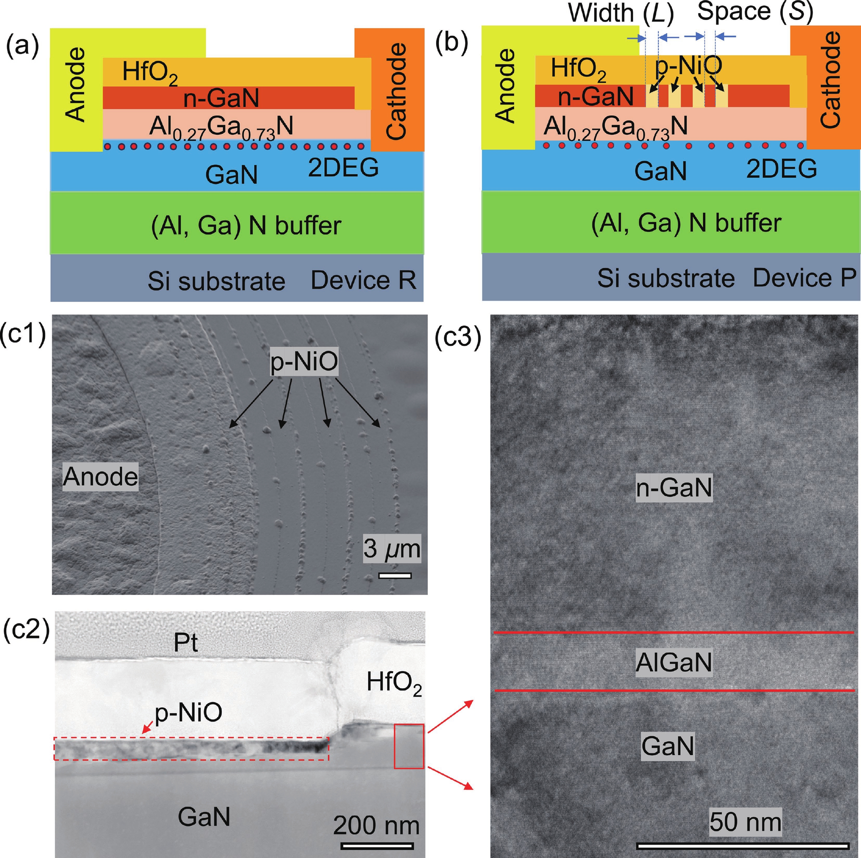
Fig. 1.  (Color online) Schematic cross-sections for (a) Device R and (b) Device P, respectively. (c1) SEM image of p-NiO structure for the Device P. (c2) Cross-sectional TEM image of the p-NiO/n-GaN junction for Device P. (c3) Zoomed-in TEM image of n-GaN/AlGaN/GaN structure.

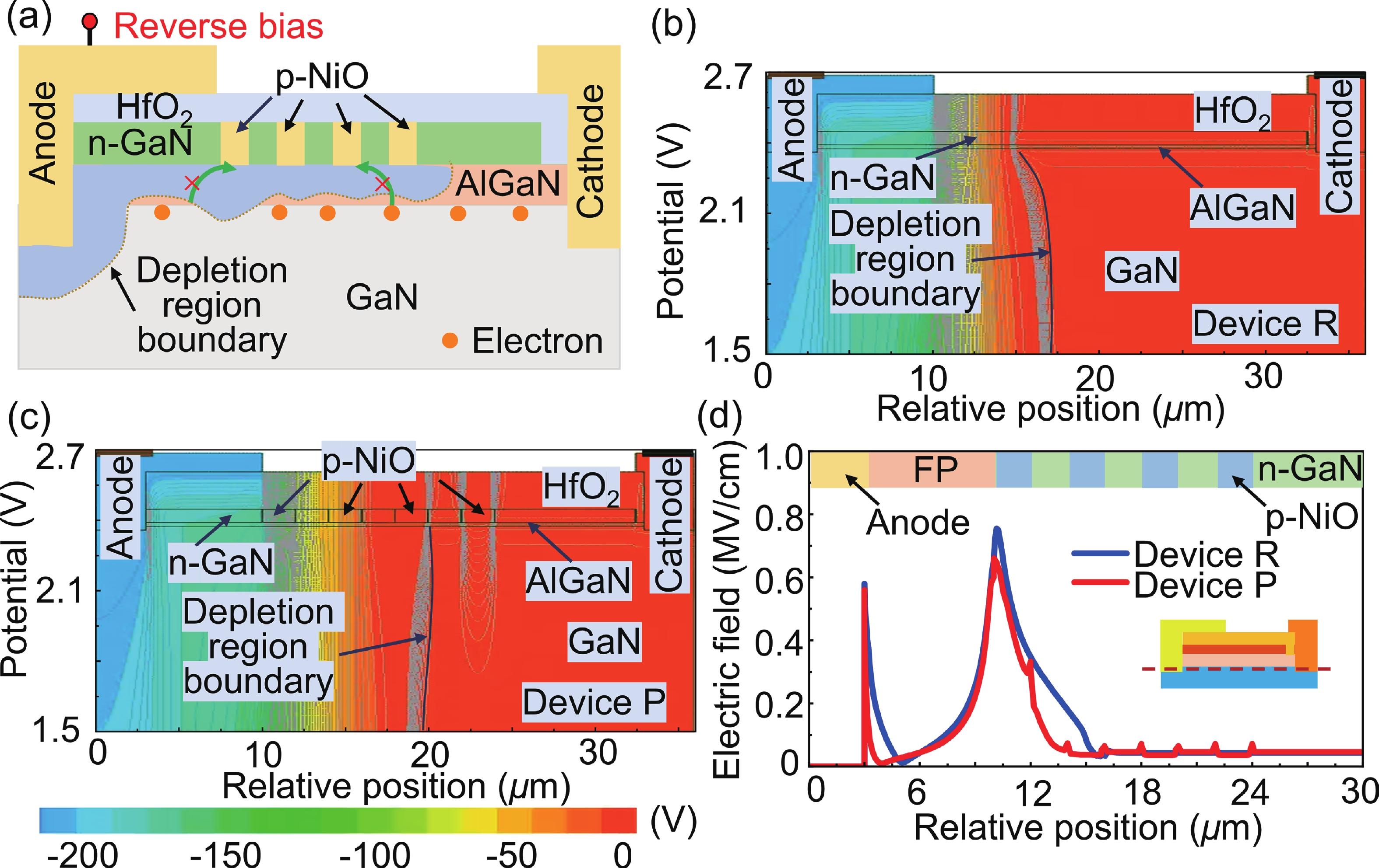
Fig. 2.  (Color online) (a) Schematic diagram of lateral junctions inhibiting the electron capture process. Simulated electrical potential distributions for (b) Device R and (c) Device P, respectively. (d) Simulated electric field profiles along the horizontal direction for Devices R and P at the reverse voltage of −200 V.

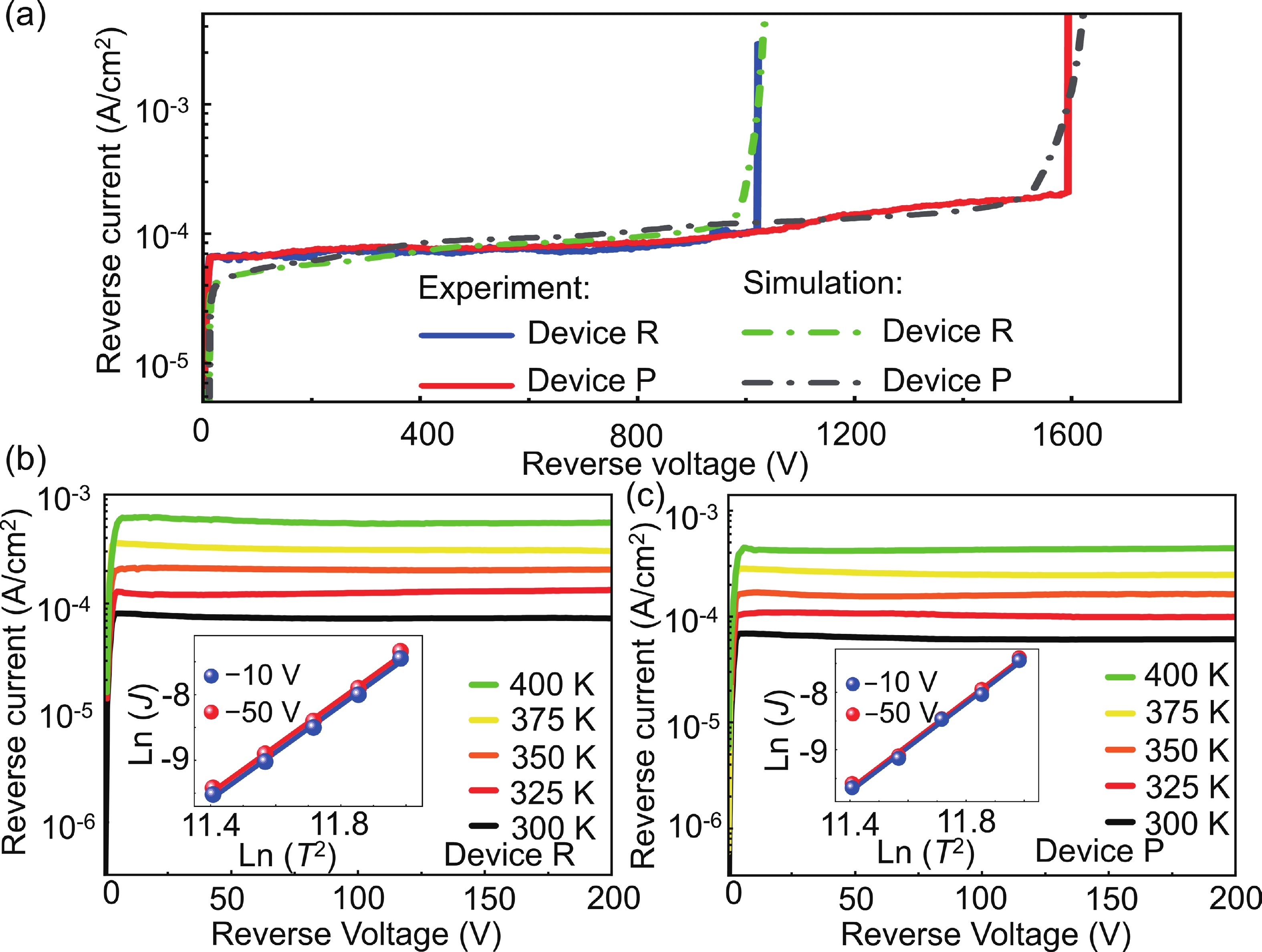
Fig. 3.  (Color online) (a) Measured and simulated reverse JV characteristics for Devices R and P. Measured leakage current as the function of reverse bias at different temperatures from 300 to 400 K for (b) Device R and (c) Device P, respectively. Insets in Figs. 3(b) and (c) linear relationship between Ln(J) and Ln(T 2).

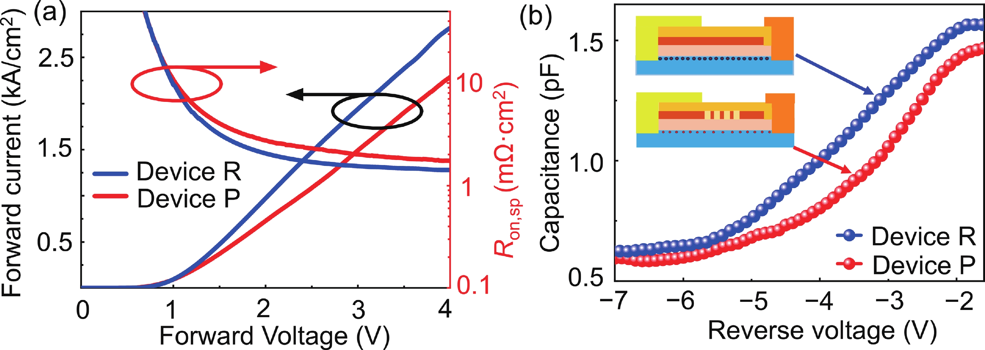
Fig. 4.  (Color online) (a) Measured forward JV characteristics and calculated Ron,sp for Devices R and P. (b) Measured C−V characteristics for Devices R and P.

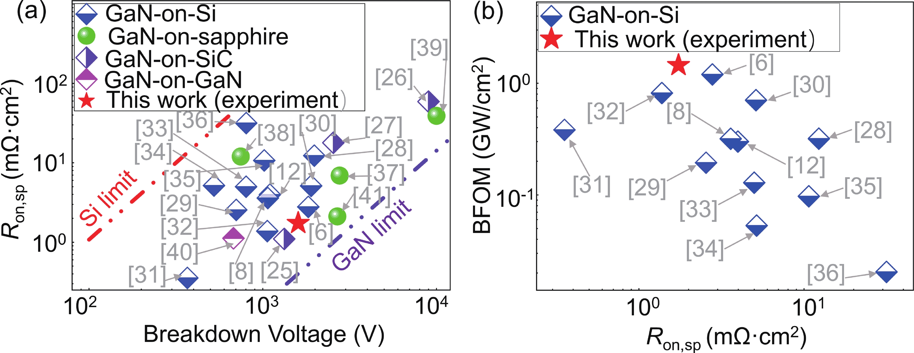
Fig. 5.  (Color online) Benchmark plot for (a) BV in terms of Ron,sp and (b) Ron,sp in terms of BFOM for Device P and other reported AlGaN/GaN power devices.

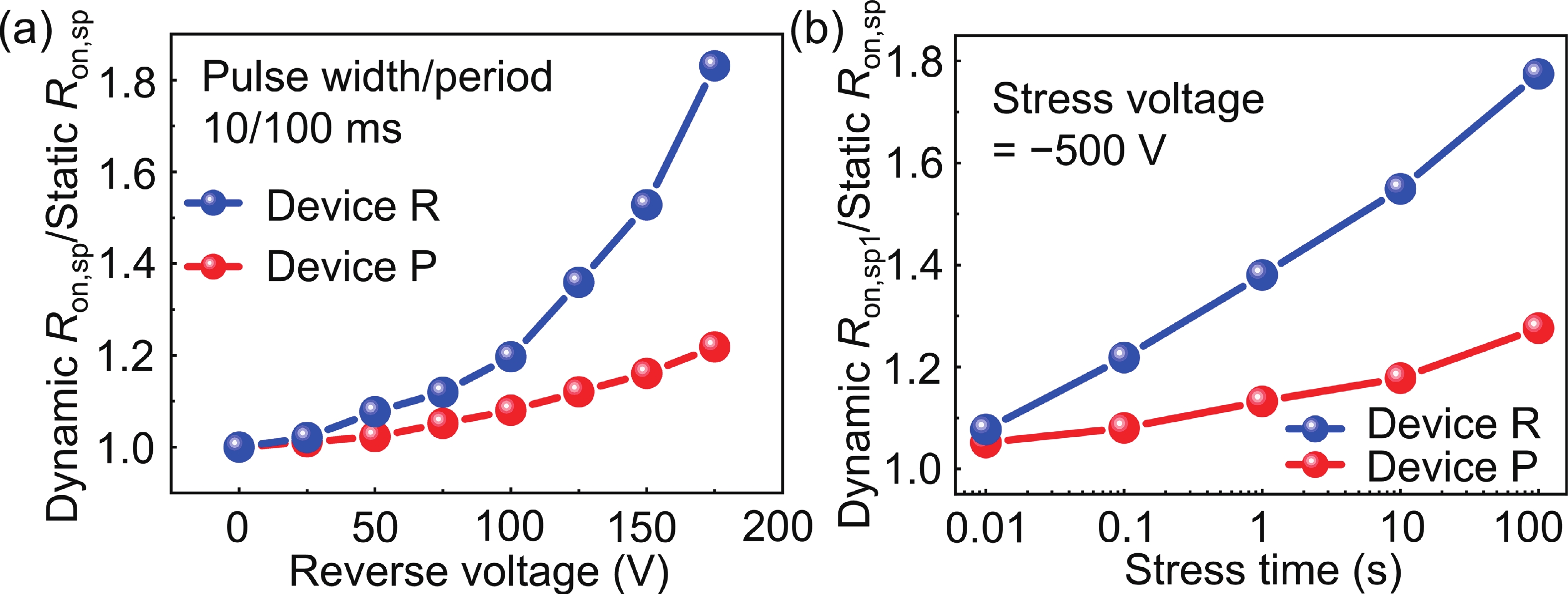
Fig. 6.  (Color online) (a) Measured dynamic Ron,sp/static Ron,sp as a function of different electrical stresses. (b) Measured dynamic Ron,sp1/static Ron,sp as a function of the reverse stress duration.

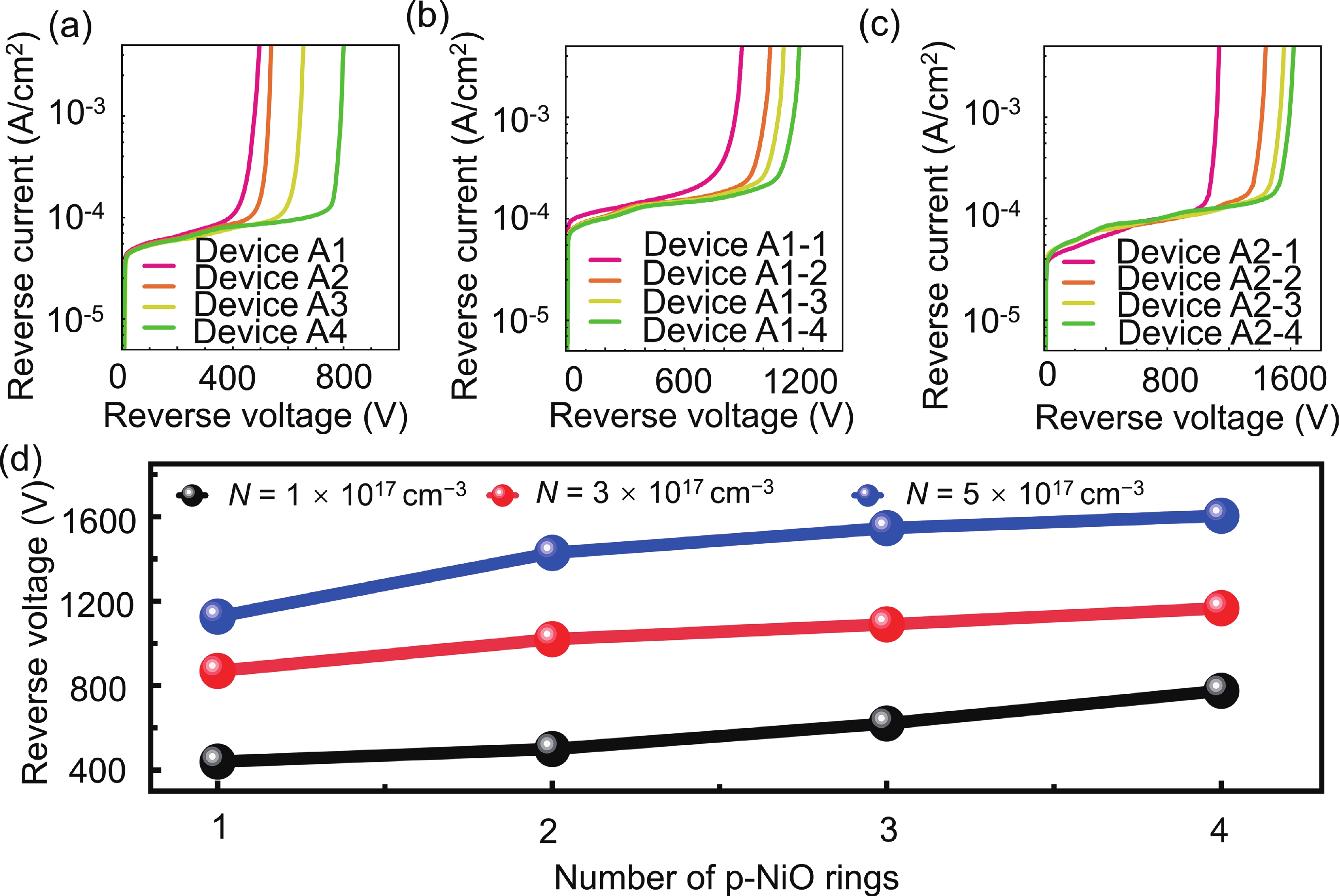
Fig. 7.  (Color online) (a)−(c) Simulated reverse JV characteristics for AlGaN/GaN-based SBDs with different N and number of p-NiO rings, respectively. (d) BV as a function of number of p-NiO rings for SBDs with different N extracted from numerical simulation.

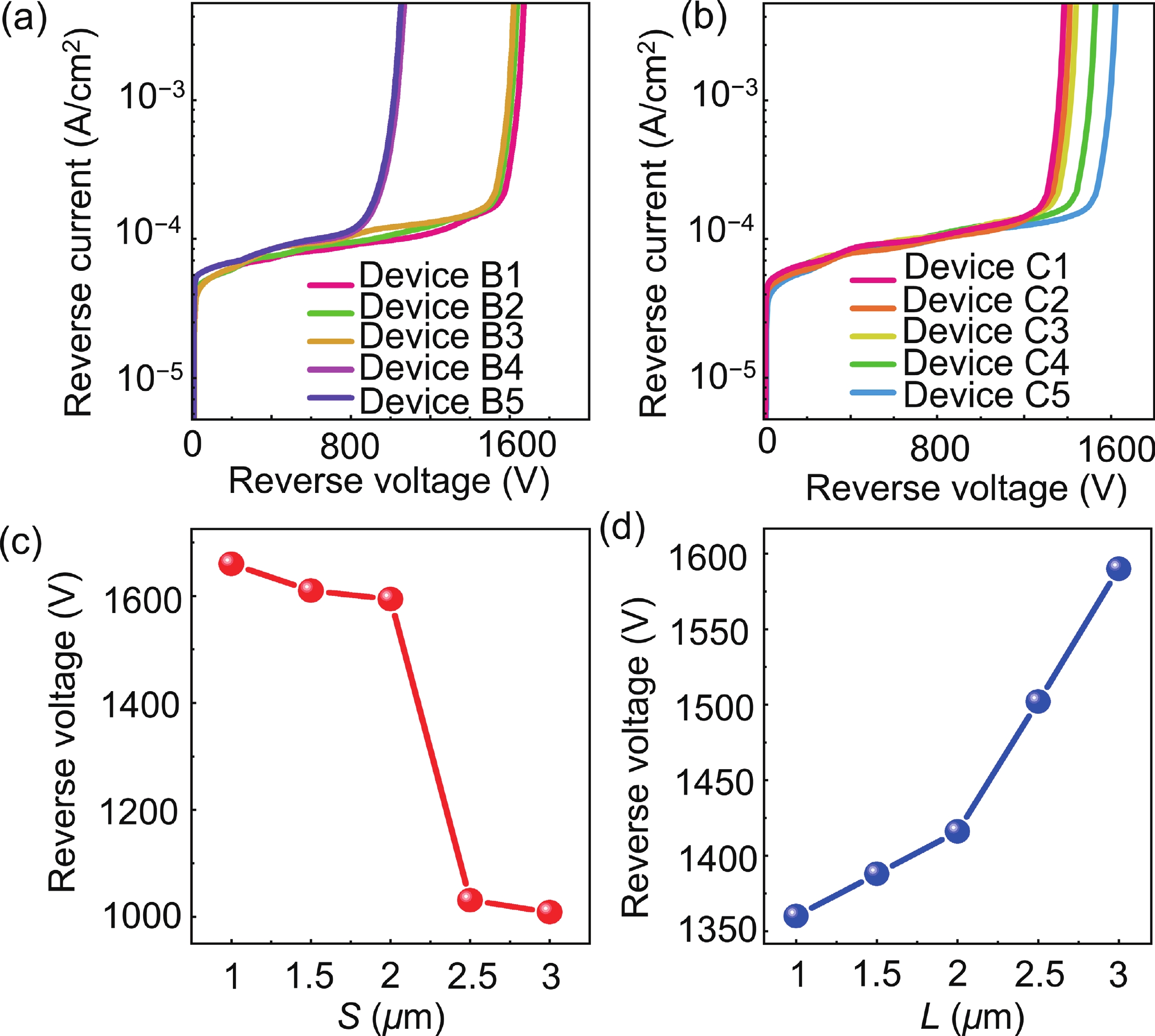
Fig. 8.  (Color online) Simulated reverse JV characteristics for SBDs with different (a) S and (b) L. BV as a function of S for (c) Devices B1−B5 and L for (d) Devices C1−C5.

Table 1.   Comparison of dynamic Ron,sp degradation under reverse-bias stress for Device P and other reported AlGaN/GaN power devices

ReferencesSubstratesStress voltage (V)Stress time (s)Pulse width/period (ms)ΔRon,sp (%)
[42]Sapphire−25010/10021.3
[42]Sapphire−600108.6
[43]Si−1005/10035
[6]Si−5000.135
[44]Si−1002/123.5
[44]Si−1002/1216
This workSi−50010027
This workSi−17510/10020
ΔRon,sp (%) = (dynamic Ron,sp / static Ron,sp − 1) × 100%.
DownLoad: CSV

Table 2.   Structural parameters for devices with different p-NiO ring designs

N (cm−3)L (μm)S (μm)Number of rings
Device A11 × 1017221
Device A21 × 1017222
Device A31 × 1017223
Device A41 × 1017224
Device A1-13 × 1017221
Device A1-23 × 1017222
Device A1-33 × 1017223
Device A1-43 × 1017224
Device A2-15 × 1017221
Device A2-25 × 1017222
Device A2-35 × 1017223
Device A2-45 × 1017224
Device B15 × 1017214
Device B25 × 101721.54
Device B35 × 1017224
Device B45 × 101722.54
Device B55 × 1017234
Device C15 × 1017124
Device C25 × 10171.524
Device C35 × 1017224
Device C45 × 10172.524
Device C55 × 1017324
DownLoad: CSV
[1]
Teo K H, Zhang Y H, Chowdhury N, et al. Emerging GaN technologies for power, RF, digital, and quantum computing applications: Recent advances and prospects. J Appl Phys, 2021, 130(16): 160902 doi: 10.1063/5.0061555
[2]
Buffolo M, Favero D, Marcuzzi A, et al. Review and outlook on GaN and SiC power devices: Industrial state-of-the-art, applications, and perspectives. IEEE Trans Electron Devices, 2024, 71(3): 1344 doi: 10.1109/TED.2023.3346369
[3]
Zhou Q, Jin Y, Shi Y Y, et al. High reverse blocking and low onset voltage AlGaN/GaN-on-Si lateral power diode with MIS-gated hybrid anode. IEEE Electron Device Lett, 2015, 36(7): 660 doi: 10.1109/LED.2015.2432171
[4]
Tao M, Wang M J, Wen C P, et al. Kilovolt GaN MOSHEMT on silicon substrate with breakdown electric field close to the theoretical limit. 2017 29th International Symposium on Power Semiconductor Devices and IC’s (ISPSD). Sapporo, Japan. IEEE, 2017: 93
[5]
Nela L, Yildirim H K, Erine C, et al. Conformal passivation of multi-channel GaN power transistors for reduced current collapse. IEEE Electron Device Lett, 2021, 42(1): 86 doi: 10.1109/LED.2020.3038808
[6]
Zhang T, Li R H, Lu J, et al. A 0.43 V/90 nA/mm lateral AlGaN/GaN Schottky barrier diode with plasma-free groove anode technique. IEEE Electron Device Lett, 2021, 42(12): 1747 doi: 10.1109/LED.2021.3123652
[7]
Wong M S, Lee C M, Myers D J, et al. Size-independent peak efficiency of III-nitride micro-light-emitting-diodes using chemical treatment and sidewall passivation. Appl Phys Express, 2019, 12(9): 097004 doi: 10.7567/1882-0786/ab3949
[8]
Wang H Y, Mao W, Yang C, et al. Lateral AlGaN/GaN Schottky barrier diode with arrayed p-GaN islands termination. IEEE Trans Electron Devices, 2021, 68(12): 6046 doi: 10.1109/TED.2021.3118326
[9]
Soni A, Amogh K M, Shrivastava M. Design guidelines and performance tradeoffs in recessed AlGaN/GaN Schottky barrier diodes. IEEE Trans Electron Devices, 2020, 67(11): 4834 doi: 10.1109/TED.2020.3024354
[10]
Lee H S, Kalarickal N K, Rahman M W, et al. High-permittivity dielectric edge termination for vertical high voltage devices. J Comput Electron, 2020, 19(4): 1538 doi: 10.1007/s10825-020-01553-y
[11]
Wang Z Z, Huang F P, Chu C S, et al. 2.5 kV/1.95 GW/cm2 AlGaN/GaN-based lateral Schottky barrier diodes with a high-k field plate to reduce reverse current. IEEE Trans Electron Devices, 2024, 71(6): 3811 doi: 10.1109/TED.2024.3388377
[12]
He J T, Wang Z Z, Huang F P, et al. Physical model development for fabricating MIS-anode-based 1100 V AlGaN/GaN-based lateral Schottky barrier diodes grown on silicon substrate with low leakage current. Adv Electron Mater, 2025, 11(13): 2500111 doi: 10.1002/aelm.202500111
[13]
Xu T, Tang Z Q, Zhou Z Y, et al. Simulation optimization of AlGaN/GaN SBD with field plate structures and recessed anode. Micromachines, 2023, 14(6): 1121 doi: 10.3390/mi14061121
[14]
Shi Y T, Ren F F, Xu W Z, et al. Realization of p-type gallium nitride by magnesium ion implantation for vertical power devices. Sci Rep, 2019, 9: 8796 doi: 10.1038/s41598-019-45177-0
[15]
Guo H, Gong H H, Shao P F, et al. Over 1200 V normally-OFF p-NiO gated AlGaN/GaN HEMTs on Si with a small threshold voltage shift. IEEE Electron Device Lett, 2022, 43(2): 268 doi: 10.1109/LED.2021.3137510
[16]
Qin Y, Xiao M, Zhang R Z, et al. 1 kV GaN-on-Si quasi-vertical Schottky rectifier. IEEE Electron Device Lett, 2023, 44(7): 1052 doi: 10.1109/LED.2023.3282025
[17]
Huang F P, Chu C S, Wang Z Z, et al. GaN-based quasi-vertical Schottky barrier diode hybridized with p-NiO layer to achieve 1.1 kV breakdown voltage and enhance the current spreading effect. Appl Phys Express, 2022, 15(8): 084001 doi: 10.35848/1882-0786/ac7eac
[18]
Khadar R A, Floriduz A, Wang T F, et al. P-NiO junction termination extensions for GaN power devices. Appl Phys Express, 2021, 14(7): 071006 doi: 10.35848/1882-0786/ac09ff
[19]
Li S C, Yang S, Han Z, et al. Vertical GaN Schottky barrier diode with hybrid P-NiO junction termination extension. IEEE J Electron Devices Soc, 2024, 12: 548 doi: 10.1109/JEDS.2024.3432783
[20]
Gong H H, Yu X X, Xu Y, et al. β-Ga2O3 vertical heterojunction barrier Schottky diodes terminated with p-NiO field limiting rings. Appl Phys Lett, 2021, 118(20): 202102 doi: 10.1063/5.0050919
[21]
Xiao M, Ma Y W, Du Z H, et al. First demonstration of vertical superjunction diode in GaN. 2022 International Electron Devices Meeting (IEDM). San Francisco, CA, USA. IEEE, 2022: 35.6. 1
[22]
Malik R R, Karthik S R, Joshi V, et al. Experimental validation of buffer traps-driven electric field dynamics governing breakdown and leakage trends in AlGaN/GaN heterostructures. 2025 IEEE International Reliability Physics Symposium (IRPS). Monterey, CA, USA. IEEE, 2025: P26. GaN
[23]
Wang Z Z, He J T, Huang F P, et al. AlGaN/GaN-based SBDs grown on silicon substrates with trenched n+-GaN cap layer and local passivation layer to improve BFOM and dynamic properties. J Semicond, 2025, 46(9): 092502 doi: 10.1088/1674-4926/25010024
[24]
Wang Z Z, Huang F P, Chu C S, et al. On the super-junction formed by using field plate for lateral AlGaN/GaN-based Schottky barrier diodes. Jpn J Appl Phys, 2023, 62(9): 094001 doi: 10.35848/1347-4065/acf17a
[25]
Rahman M W, Chandrasekar H, Razzak T, et al. Hybrid BaTiO3/SiNx/AlGaN/GaN lateral Schottky barrier diodes with low turn-on and high breakdown performance. Appl Phys Lett, 2021, 119: 013504 doi: 10.1063/5.0055946
[26]
Colón A, Douglas E A, Pope A J, et al. Demonstration of a 9 kV reverse breakdown and 59 mΩ-cm2 specific on-resistance AlGaN/GaN Schottky barrier diode. Solid State Electron, 2019, 151: 47 doi: 10.1016/j.sse.2018.10.009
[27]
Zhang T, Zhang Y N, Li R H, et al. Current transport mechanism of AlGaN-channel Schottky barrier diode with extremely low leakage current and high blocking voltage of 2.55 kV. Appl Phys Lett, 2022, 120(9): 092102 doi: 10.1063/5.0077691
[28]
Deng S, Liu K, Wang C, et al. The influence of recessed floating metal rings structure on electrical properties of AlGaN/GaN Schottky barrier diodes. Phys Status Solidi A, 2022, 219(2): 2100502 doi: 10.1002/pssa.202100502
[29]
Lei J C, Wei J, Tang G F, et al. 650-V double-channel lateral Schottky barrier diode with dual-recess gated anode. IEEE Electron Device Lett, 2018, 39(2): 260 doi: 10.1109/LED.2017.2783908
[30]
Zhu M D, Song B, Qi M, et al. 1.9-kV AlGaN/GaN lateral Schottky barrier diodes on silicon. IEEE Electron Device Lett, 2015, 36(4): 375 doi: 10.1109/LED.2015.2404309
[31]
Zhu L Y, Zhou Q, Yang X, et al. High-performance ultrathin-barrier AlGaN/GaN hybrid anode diode with Al2O3 gate dielectric and In situ Si3N4-cap passivation. IEEE Trans Electron Devices, 2020, 67(10): 4136 doi: 10.1109/TED.2020.3018416
[32]
Huang F P, Mi W J, He J T, et al. 1.06-kV polarization gate-assisted Si-based AlGaN/GaN Schottky barrier diode with 0.817-GW/cm2 BFOM and 10–5-A/cm2 Leakage current. IEEE Trans Electron Devices, 2025, 72(12): 6918 doi: 10.1109/TED.2025.3618521
[33]
Lee H S, Jung D Y, Park Y, et al. 0.34 VT AlGaN/GaN-on-Si large Schottky barrier diode with recessed dual anode metal. IEEE Electron Device Lett, 2015, 36(11): 1132 doi: 10.1109/LED.2015.2475178
[34]
Ha M W, Han M K, Hahn C K. Effects of post-oxidation on leakage current of high-voltage AlGaN/GaN Schottky barrier diodes on Si(111) substrates. Solid State Electron, 2013, 81: 1 doi: 10.1016/j.sse.2012.11.006
[35]
Chang T F, Huang C F, Yang T Y, et al. Low Turn-on voltage dual metal AlGaN/GaN Schottky barrier diode. Solid State Electron, 2015, 105: 12 doi: 10.1016/j.sse.2014.11.024
[36]
Chiu H C, Chen S C, Chiu J W, et al. AlGaN/GaN Schottky barrier diodes on silicon substrates with various Fe doping concentrations in the buffer layers. Microelectron Reliab, 2018, 83: 238 doi: 10.1016/j.microrel.2017.05.034
[37]
Lu Y, Zhou F, Xu W Z, et al. Multi-aperture anode based AlGaN/GaN Schottky barrier diodes with low turn-on voltage and high uniformity. Appl Phys Express, 2020, 13(9): 096502 doi: 10.35848/1882-0786/abaf0e
[38]
Lee J H, Park C, Im K S, et al. AlGaN/GaN-based lateral-type Schottky barrier diode with very low reverse recovery charge at high temperature. IEEE Trans Electron Devices, 2013, 60(10): 3032 doi: 10.1109/TED.2013.2273271
[39]
Xiao M, Ma Y W, Liu K, et al. 10 kV, 39 mΩ·cm2 multi-channel AlGaN/GaN Schottky barrier diodes. IEEE Electron Device Lett, 2021, 42(6): 808 doi: 10.1109/LED.2021.3076802
[40]
Pu T F, Wang H C, Hsueh K P, et al. AlGaN/GaN Schottky barrier diodes on free-standing GaN substrates with a Si doped barrier layer. IEEE J Electron Devices Soc, 2022, 10: 318 doi: 10.1109/JEDS.2022.3165534
[41]
Wei X, Shen W C, Zhou X, et al. 2.69 kV/2.11 mΩ·cm2 and low leakage p-GaN stripe array gated hybrid anode diodes with low turn-on voltage. IEEE Electron Device Lett, 2023, 44(1): 13 doi: 10.1109/LED.2022.3220600
[42]
Zhang T, Lv Y G, Li R H, et al. Current-collapse suppression of high-performance lateral AlGaN/GaN Schottky barrier diodes by a thick GaN cap layer. IEEE Electron Device Lett, 2021, 42(4): 477 doi: 10.1109/LED.2021.3057917
[43]
Zhang T, Li R H, Su K, et al. Proton irradiation-induced dynamic characteristics on high performance GaN/AlGaN/GaN Schottky barrier diodes. Chin Phys B, 2023, 32(8): 087301 doi: 10.1088/1674-1056/acbded
[44]
Ki R S, Lee J G, Cha H Y, et al. The effect of edge-terminated structure for lateral AlGaN/GaN Schottky barrier diodes with gated ohmic anode. Solid State Electron, 2020, 166: 107768 doi: 10.1016/j.sse.2020.107768
  • Search

    Advanced Search >>

    GET CITATION

    shu

    Export: BibTex EndNote

    Article Metrics

    Article views: 5 Times PDF downloads: 2 Times Cited by: 0 Times

    History

    Received: 09 May 2026 Revised: 17 June 2026 Online: Accepted Manuscript: 30 July 2026

    Catalog

      Email This Article

      User name:
      Email:*请输入正确邮箱
      Code:*验证码错误
      Jingting He, Zhizhong Wang, Wenjie Mi, Qiong Zhang, Fuping Huang, Chunshuang Chu, Kangkai Tian, Haoyan Liu, Yonghui Zhang, Shuting Cai, Xiao Wei Sun, Zihui Zhang. 1.6 kV/ 1.47 GW·cm−2 AlGaN/GaN-based Schottky barrier diodes grown on Si substrate with n-GaN/p-NiO/n-GaN lateral junctions[J]. Journal of Semiconductors, 2026, In Press. doi: 10.1088/1674-4926/26050011 ****J T He, Z Z Wang, W J Mi, Q Zhang, F P Huang, C S Chu, K K Tian, H Y Liu, Y H Zhang, S T Cai, X W Sun, and Z H Zhang, 1.6 kV/ 1.47 GW·cm−2 AlGaN/GaN-based Schottky barrier diodes grown on Si substrate with n-GaN/p-NiO/n-GaN lateral junctions[J]. J. Semicond., 2026, accepted doi: 10.1088/1674-4926/26050011
      Citation:
      Jingting He, Zhizhong Wang, Wenjie Mi, Qiong Zhang, Fuping Huang, Chunshuang Chu, Kangkai Tian, Haoyan Liu, Yonghui Zhang, Shuting Cai, Xiao Wei Sun, Zihui Zhang. 1.6 kV/ 1.47 GW·cm−2 AlGaN/GaN-based Schottky barrier diodes grown on Si substrate with n-GaN/p-NiO/n-GaN lateral junctions[J]. Journal of Semiconductors, 2026, In Press. doi: 10.1088/1674-4926/26050011 ****
      J T He, Z Z Wang, W J Mi, Q Zhang, F P Huang, C S Chu, K K Tian, H Y Liu, Y H Zhang, S T Cai, X W Sun, and Z H Zhang, 1.6 kV/ 1.47 GW·cm−2 AlGaN/GaN-based Schottky barrier diodes grown on Si substrate with n-GaN/p-NiO/n-GaN lateral junctions[J]. J. Semicond., 2026, accepted doi: 10.1088/1674-4926/26050011

      1.6 kV/ 1.47 GW·cm−2 AlGaN/GaN-based Schottky barrier diodes grown on Si substrate with n-GaN/p-NiO/n-GaN lateral junctions

      DOI: 10.1088/1674-4926/26050011
      CSTR: 32376.14.1674-4926.26050011
      More Information
      • Jingting He received her bachelor’s and master’s degrees from China University of Petroleum in 2015 and 2018, respectively. She is currently a Ph.D. candidate at Guangdong University of Technology. Her research primarily focuses on the design and fabrication for gallium nitride power semiconductor devices
      • Zhizhong Wang received his Ph.D. from Hebei University of Technology. He is currently a faculty member at the School of Physics and Electronic Engineering, Shan Xi University. His research primarily focuses on the design and fabrication for gallium nitride power semiconductor devices
      • Zihui Zhang received his B. S. from Shandong University and Ph.D. from Nanyang Technological University. Before he joined Guangdong University of Technology as a Distinguished Professor, he was a Professor at Hebei University of Technology. He is also a “100-Talent-Plan” Distinguished Professor of Hebei Province. His research interests include III-nitride-based semiconductor materials and devices, semiconductor device physics, device modeling and simulation
      • Corresponding author: zh.zhang@hebut.edu.cn
      • Received Date: 2026-05-09
      • Revised Date: 2026-06-17
      • Available Online: 2026-07-30

      Catalog

        /

        DownLoad:  Full-Size Img  PowerPoint
        Return
        Return