


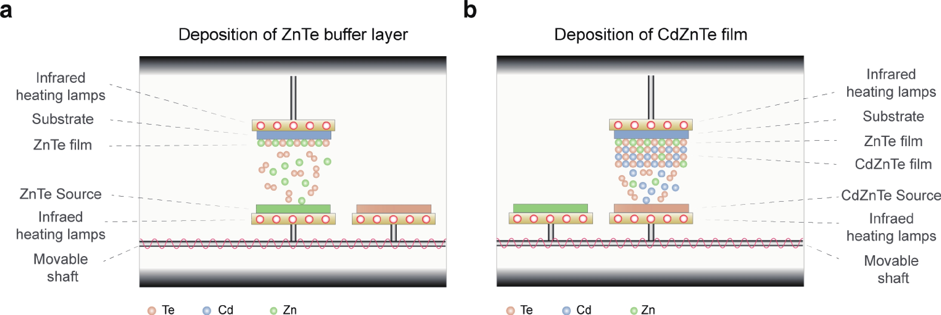
Fig. 1.
(Color online) Schematic diagram of CSS system. (a) Schematic diagram of CSS system during the deposition of ZnTe buffer layer. (b) Schematic diagram of CSS system during the deposition of CdZnTe film.
ARTICLES
Mengshi Yu1, 2, 3, , Qing Hu2, 3, Mengqi Wu2, 3, Yuecong Liu2, 3, Silong Liu2, 3, Siqi Hu2, 3, Jian Hao2, 3, Song Zhu2, 3 and Yangyang Huai2, 3,
Corresponding author: Mengshi Yu, yums-cnc@pku.edu.cn; Yangyang Huai, yyhuai1987@gmail.com
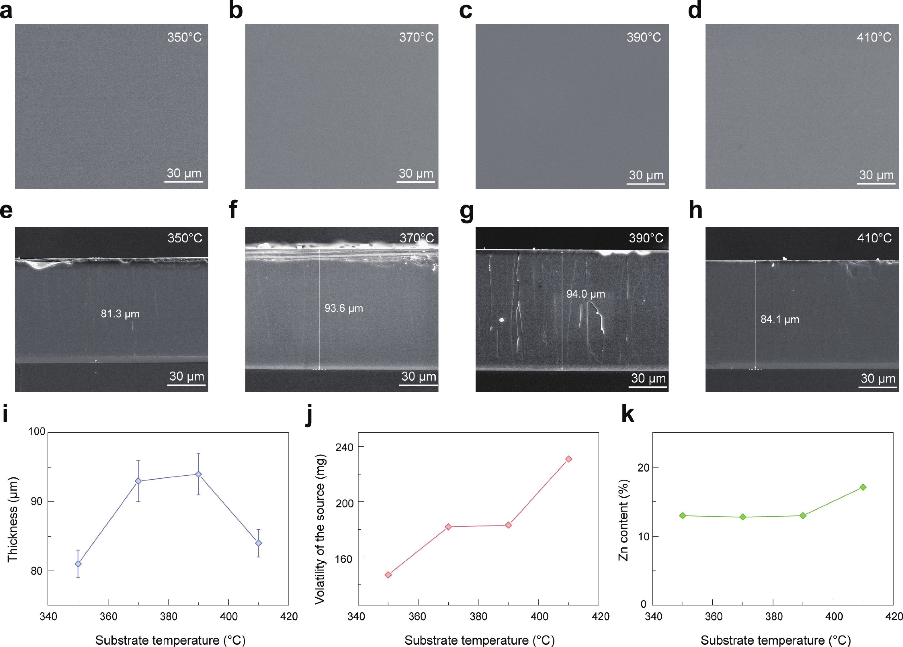
Abstract: CdZnTe films show great promise for applications in infrared imaging, solar cells, and radiation detection due to their excellent optoelectronic properties. However, single-crystal CdZnTe films directly deposited on commercial GaAs (001) substrate suffer from a high density of crystalline defects caused by a large lattice mismatch. Here we report the epitaxial growth of single-crystal CdZnTe films on GaAs (001) substrate using close spaced sublimation with a single-crystal ZnTe thin film as a buffer layer. As-grown CdZnTe films exhibit higher crystalline quality than those grown without a buffer layer. The optimal substrate temperature range is found to be 370-390 °C, and the growth rate reaches 94 μm/h. This work provides an approach to grow high-quality single-crystal CdZnTe films for optoelectronic device applications.
Keywords: single-crystal CdZnTe films, GaAs (001) substrate, ZnTe thin film, buffer layer
| [1] |
Lei W, Antoszewski J, Faraone L. Progress, challenges, and opportunities for HgCdTe infrared materials and detectors. Appl Phys Rev, 2015, 2(4): 041303 doi: 10.1063/1.4936577
|
| [2] |
Li F Z, Deng J, Zhou J, et al. HgCdTe mid-Infrared photo response enhanced by monolithically integrated meta-lenses. Sci Rep, 2020, 10(1): 6372 doi: 10.1038/s41598-020-62433-w
|
| [3] |
Bashir K, Mehboob N, Ali A, et al. Fabrication and characterization of Cd1–xZnxTe thin films for photovoltaic applications. Mater Lett, 2021, 304: 130737 doi: 10.1016/j.matlet.2021.130737
|
| [4] |
Sharma R, Chuhadiya S, Kamlesh, et al. CdZnTe thin films as proficient absorber layer candidates in solar cell devices: A review. Energy Adv, 2023, 2(12): 1980 doi: 10.1039/D3YA00120B
|
| [5] |
Hou B, Chen Q S, Yi L Y, et al. Materials innovation and electrical engineering in X-ray detection. Nat Rev Electr Eng, 2024, 1(10): 639 doi: 10.1038/s44287-024-00086-x
|
| [6] |
Abbene L, Principato F, Gerardi G, et al. Room-temperature X-ray response of cadmium-zinc-telluride pixel detectors grown by the vertical Bridgman technique. J Synchrotron Rad, 2020, 27(2): 319 doi: 10.1107/S1600577519015996
|
| [7] |
Jiang R, Shi J S, Kang Y, et al. High-performance CZT X-ray imaging device with ultrahigh sensitivity and ultralow detection limit. J Alloys Compd, 2025, 1040: 183346 doi: 10.1016/j.jallcom.2025.183346
|
| [8] |
Gao X Y, Sun H, Yang D Y, et al. Large-area CdZnTe thick film based array X-ray detector. Vacuum, 2021, 183: 109855 doi: 10.1016/j.vacuum.2020.109855
|
| [9] |
Danielsson M, Persson M, Sjölin M. Photon-counting X-ray detectors for CT. Phys Med Biol, 2021, 66(3): 03TR01 doi: 10.1088/1361-6560/abc5a5
|
| [10] |
Wang Q F, Huang H F, Xu K, et al. Enhancement of detection performances of cadmium zinc telluride (CdZnTe) radiation detectors through sapphire substrates. J Alloys Compd, 2025, 1010: 177952 doi: 10.1016/j.jallcom.2024.177952
|
| [11] |
Li Y, Cao K, Zha G, et al. An alternative GaSb substrate allowing close-spaced sublimation of Cd0.9Zn0.1Te epitaxial thick film for radiation detectors. Mater Sci Semicond Process, 2022, 147: 106688 doi: 10.1016/j.mssp.2022.106688
|
| [12] |
Wan X, Cao K, Li Y, et al. Preparation and characterization of large-sized CdZnTe epitaxial single crystal. Nucl Instrum Meth Phys Res Sect A Accel Spectrometers Detect Assoc Equip, 2023, 1056: 168625 doi: 10.1016/j.nima.2023.168625
|
| [13] |
Wu S H, Zha G Q, Cao K, et al. The growth of CdZnTe epitaxial thick film by close spaced sublimation for radiation detector. Vacuum, 2019, 168: 108852 doi: 10.1016/j.vacuum.2019.108852
|
| [14] |
Liu Y, Zha G Q, Cao K, et al. Growth of CdZnTe (2 1 1) epilayers on GaAs by close spaced sublimation as an alternative substrate for HgCdTe growth. Infrared Phys Technol, 2023, 133: 104857 doi: 10.1016/j.infrared.2023.104857
|
| [15] |
Liu Y, Wu W, Zhang X L, et al. Investigation of the CdZnTe (2 1 1) and (1 3 3) films grown on GaAs (2 1 1) controlled by temperature: Experiment and first-principles calculations. Appl Surf Sci, 2024, 649: 159154 doi: 10.1016/j.apsusc.2023.159154
|
| [16] |
Cao K, Jie W Q, Zha G Q, et al. Origin and evolution of threading dislocation in CdZnTe (0 0 1)/GaAs (0 0 1) epilayer grown by close spaced sublimation. Appl Surf Sci, 2020, 504: 144431 doi: 10.1016/j.apsusc.2019.144431
|
| [17] |
Cheng R Y, Cao K, Zha G Q, et al. Formation mechanism and elimination of needle defects on CdZnTe epitaxial films prepared by close-spaced sublimation. Appl Surf Sci, 2024, 657: 159813 doi: 10.1016/j.apsusc.2024.159813
|
| [18] |
Cao K, Jie W Q, Zha G Q, et al. Analysis of dislocations in CdZnTe epitaxial film with kelvin probe and conductive atomic force microscopy. J Electron Mater, 2020, 49(6): 3907 doi: 10.1007/s11664-020-08094-x
|
| [19] |
Cao K, Jie W Q, Zha G Q, et al. Improvement of crystalline quality of CdZnTe epilayers on GaAs (001) substrates with a two-step growth by Close Spaced Sublimation. Vacuum, 2019, 164: 319 doi: 10.1016/j.vacuum.2019.03.036
|
| [20] |
Tian X, Tan T T, Cao K, et al. Effects of homogeneous buffer layer on the crystalline quality and electrical properties of CdZnTe epitaxial films. IEEE Trans Electron Devices, 2025, 72(3): 1235 doi: 10.1109/TED.2025.3531320
|
| [21] |
Xu K, Huang H F, Wang Q F, et al. Effect of a seed layer on the properties of CdZnTe thick films prepared by close-spaced sublimation method. Mater Sci Semicond Process, 2025, 186: 109054 doi: 10.1016/j.mssp.2024.109054
|
| [22] |
Cao K, Zha G Q, Zhang H, et al. Preparation of Cd0.8Zn0.2Te/Cd0.5Zn0.5Te/n+-GaAs thick film radiation detectors by close spaced sublimation. Vacuum, 2021, 192: 110426 doi: 10.1016/j.vacuum.2021.110426
|
| [23] |
Sun J H, Shen Y, Chen R Z, et al. Effect of ZnTe transition layer to the performance of CdZnTe/GaN multilayer films for solar-blind photodetector applications. J Phys D Appl Phys, 2020, 53(41): 415105 doi: 10.1088/1361-6463/ab9331
|
| [24] |
Liu Y, Zhang X L, Gao Z H, et al. Growth of high quality CdZnTe (133) epilayers on GaAs (211) substrate with Zn1–xCdxTe/ZnTe buffer layer by close spaced sublimation. J Alloys Compd, 2024, 977: 173261 doi: 10.1016/j.jallcom.2023.173261
|
| [25] |
Liu Y, Wu W, Yang S, et al. Investigation of the growth of high quality CdZnTe(211) films with ZnTe buffer layer: Experiment and first-principles calculations. Appl Surf Sci, 2026, 715: 164484 doi: 10.1016/j.apsusc.2025.164484
|
| [26] |
Li Y, Zhang X L, Wan X, et al. Improvement of crystallinity of CdZnTe epilayers on GaSb substrates by ZnTe buffer layer. Vacuum, 2023, 217: 112551 doi: 10.1016/j.vacuum.2023.112551
|
| [27] |
Xu H T, Xu R, Huang J, et al. The dependence of Zn content on thermal treatments for Cd1–xZnxTe thin films deposited by close-spaced sublimation. Appl Surf Sci, 2014, 305: 477 doi: 10.1016/j.apsusc.2014.03.117
|
| [28] |
Zhang L N, Dong J C, Ding F. Strategies, status, and challenges in wafer scale single crystalline two-dimensional materials synthesis. Chem Rev, 2021, 121(11): 6321 doi: 10.1021/acs.chemrev.0c01191
|
| [1] |
Lei W, Antoszewski J, Faraone L. Progress, challenges, and opportunities for HgCdTe infrared materials and detectors. Appl Phys Rev, 2015, 2(4): 041303 doi: 10.1063/1.4936577
|
| [2] |
Li F Z, Deng J, Zhou J, et al. HgCdTe mid-Infrared photo response enhanced by monolithically integrated meta-lenses. Sci Rep, 2020, 10(1): 6372 doi: 10.1038/s41598-020-62433-w
|
| [3] |
Bashir K, Mehboob N, Ali A, et al. Fabrication and characterization of Cd1–xZnxTe thin films for photovoltaic applications. Mater Lett, 2021, 304: 130737 doi: 10.1016/j.matlet.2021.130737
|
| [4] |
Sharma R, Chuhadiya S, Kamlesh, et al. CdZnTe thin films as proficient absorber layer candidates in solar cell devices: A review. Energy Adv, 2023, 2(12): 1980 doi: 10.1039/D3YA00120B
|
| [5] |
Hou B, Chen Q S, Yi L Y, et al. Materials innovation and electrical engineering in X-ray detection. Nat Rev Electr Eng, 2024, 1(10): 639 doi: 10.1038/s44287-024-00086-x
|
| [6] |
Abbene L, Principato F, Gerardi G, et al. Room-temperature X-ray response of cadmium-zinc-telluride pixel detectors grown by the vertical Bridgman technique. J Synchrotron Rad, 2020, 27(2): 319 doi: 10.1107/S1600577519015996
|
| [7] |
Jiang R, Shi J S, Kang Y, et al. High-performance CZT X-ray imaging device with ultrahigh sensitivity and ultralow detection limit. J Alloys Compd, 2025, 1040: 183346 doi: 10.1016/j.jallcom.2025.183346
|
| [8] |
Gao X Y, Sun H, Yang D Y, et al. Large-area CdZnTe thick film based array X-ray detector. Vacuum, 2021, 183: 109855 doi: 10.1016/j.vacuum.2020.109855
|
| [9] |
Danielsson M, Persson M, Sjölin M. Photon-counting X-ray detectors for CT. Phys Med Biol, 2021, 66(3): 03TR01 doi: 10.1088/1361-6560/abc5a5
|
| [10] |
Wang Q F, Huang H F, Xu K, et al. Enhancement of detection performances of cadmium zinc telluride (CdZnTe) radiation detectors through sapphire substrates. J Alloys Compd, 2025, 1010: 177952 doi: 10.1016/j.jallcom.2024.177952
|
| [11] |
Li Y, Cao K, Zha G, et al. An alternative GaSb substrate allowing close-spaced sublimation of Cd0.9Zn0.1Te epitaxial thick film for radiation detectors. Mater Sci Semicond Process, 2022, 147: 106688 doi: 10.1016/j.mssp.2022.106688
|
| [12] |
Wan X, Cao K, Li Y, et al. Preparation and characterization of large-sized CdZnTe epitaxial single crystal. Nucl Instrum Meth Phys Res Sect A Accel Spectrometers Detect Assoc Equip, 2023, 1056: 168625 doi: 10.1016/j.nima.2023.168625
|
| [13] |
Wu S H, Zha G Q, Cao K, et al. The growth of CdZnTe epitaxial thick film by close spaced sublimation for radiation detector. Vacuum, 2019, 168: 108852 doi: 10.1016/j.vacuum.2019.108852
|
| [14] |
Liu Y, Zha G Q, Cao K, et al. Growth of CdZnTe (2 1 1) epilayers on GaAs by close spaced sublimation as an alternative substrate for HgCdTe growth. Infrared Phys Technol, 2023, 133: 104857 doi: 10.1016/j.infrared.2023.104857
|
| [15] |
Liu Y, Wu W, Zhang X L, et al. Investigation of the CdZnTe (2 1 1) and (1 3 3) films grown on GaAs (2 1 1) controlled by temperature: Experiment and first-principles calculations. Appl Surf Sci, 2024, 649: 159154 doi: 10.1016/j.apsusc.2023.159154
|
| [16] |
Cao K, Jie W Q, Zha G Q, et al. Origin and evolution of threading dislocation in CdZnTe (0 0 1)/GaAs (0 0 1) epilayer grown by close spaced sublimation. Appl Surf Sci, 2020, 504: 144431 doi: 10.1016/j.apsusc.2019.144431
|
| [17] |
Cheng R Y, Cao K, Zha G Q, et al. Formation mechanism and elimination of needle defects on CdZnTe epitaxial films prepared by close-spaced sublimation. Appl Surf Sci, 2024, 657: 159813 doi: 10.1016/j.apsusc.2024.159813
|
| [18] |
Cao K, Jie W Q, Zha G Q, et al. Analysis of dislocations in CdZnTe epitaxial film with kelvin probe and conductive atomic force microscopy. J Electron Mater, 2020, 49(6): 3907 doi: 10.1007/s11664-020-08094-x
|
| [19] |
Cao K, Jie W Q, Zha G Q, et al. Improvement of crystalline quality of CdZnTe epilayers on GaAs (001) substrates with a two-step growth by Close Spaced Sublimation. Vacuum, 2019, 164: 319 doi: 10.1016/j.vacuum.2019.03.036
|
| [20] |
Tian X, Tan T T, Cao K, et al. Effects of homogeneous buffer layer on the crystalline quality and electrical properties of CdZnTe epitaxial films. IEEE Trans Electron Devices, 2025, 72(3): 1235 doi: 10.1109/TED.2025.3531320
|
| [21] |
Xu K, Huang H F, Wang Q F, et al. Effect of a seed layer on the properties of CdZnTe thick films prepared by close-spaced sublimation method. Mater Sci Semicond Process, 2025, 186: 109054 doi: 10.1016/j.mssp.2024.109054
|
| [22] |
Cao K, Zha G Q, Zhang H, et al. Preparation of Cd0.8Zn0.2Te/Cd0.5Zn0.5Te/n+-GaAs thick film radiation detectors by close spaced sublimation. Vacuum, 2021, 192: 110426 doi: 10.1016/j.vacuum.2021.110426
|
| [23] |
Sun J H, Shen Y, Chen R Z, et al. Effect of ZnTe transition layer to the performance of CdZnTe/GaN multilayer films for solar-blind photodetector applications. J Phys D Appl Phys, 2020, 53(41): 415105 doi: 10.1088/1361-6463/ab9331
|
| [24] |
Liu Y, Zhang X L, Gao Z H, et al. Growth of high quality CdZnTe (133) epilayers on GaAs (211) substrate with Zn1–xCdxTe/ZnTe buffer layer by close spaced sublimation. J Alloys Compd, 2024, 977: 173261 doi: 10.1016/j.jallcom.2023.173261
|
| [25] |
Liu Y, Wu W, Yang S, et al. Investigation of the growth of high quality CdZnTe(211) films with ZnTe buffer layer: Experiment and first-principles calculations. Appl Surf Sci, 2026, 715: 164484 doi: 10.1016/j.apsusc.2025.164484
|
| [26] |
Li Y, Zhang X L, Wan X, et al. Improvement of crystallinity of CdZnTe epilayers on GaSb substrates by ZnTe buffer layer. Vacuum, 2023, 217: 112551 doi: 10.1016/j.vacuum.2023.112551
|
| [27] |
Xu H T, Xu R, Huang J, et al. The dependence of Zn content on thermal treatments for Cd1–xZnxTe thin films deposited by close-spaced sublimation. Appl Surf Sci, 2014, 305: 477 doi: 10.1016/j.apsusc.2014.03.117
|
| [28] |
Zhang L N, Dong J C, Ding F. Strategies, status, and challenges in wafer scale single crystalline two-dimensional materials synthesis. Chem Rev, 2021, 121(11): 6321 doi: 10.1021/acs.chemrev.0c01191
|





Article views: 3 Times PDF downloads: 0 Times Cited by: 0 Times
Received: 11 June 2026 Revised: 01 July 2026 Online: Accepted Manuscript: 10 September 2026
| Citation: |
Mengshi Yu, Qing Hu, Mengqi Wu, Yuecong Liu, Silong Liu, Siqi Hu, Jian Hao, Song Zhu, Yangyang Huai. Epitaxial growth of single-crystal CdZnTe films on GaAs (001) substrate with ZnTe buffer layer[J]. Journal of Semiconductors, 2026, In Press. doi: 10.1088/1674-4926/26060027
****
M S Yu, Q Hu, M Q Wu, Y C Liu, S L Liu, S Q Hu, J Hao, S Zhu, and Y Y Huai, Epitaxial growth of single-crystal CdZnTe films on GaAs (001) substrate with ZnTe buffer layer[J]. J. Semicond., 2026, accepted doi: 10.1088/1674-4926/26060027

|
 Mengshi Yu received her BS degree from Nanjing University of Science and Technology in 2019 and PhD degree from Peking University in 2024. She subsequently joined Jiangxi Copper Corporation Limited as a postdoctoral researcher. Her research interests focus on the epitaxial growth of semiconductor materials
 Yangyang Huai received his PhD degree from the University of Queensland in 2017 and completed his postdoctoral training in 2019. He joined Jiangxi Copper Technology Institute Co., Ltd. in 2020, where he currently serves as a Chief Researcher, Professor-level Senior Engineer, and PhD Supervisor. His research interests include the comprehensive and efficient utilization of non-ferrous and precious metal resources, as well as the controlled synthesis of high-value-added functional materials derived from these resources
| [1] |
Lei W, Antoszewski J, Faraone L. Progress, challenges, and opportunities for HgCdTe infrared materials and detectors. Appl Phys Rev, 2015, 2(4): 041303 doi: 10.1063/1.4936577
|
| [2] |
Li F Z, Deng J, Zhou J, et al. HgCdTe mid-Infrared photo response enhanced by monolithically integrated meta-lenses. Sci Rep, 2020, 10(1): 6372 doi: 10.1038/s41598-020-62433-w
|
| [3] |
Bashir K, Mehboob N, Ali A, et al. Fabrication and characterization of Cd1–xZnxTe thin films for photovoltaic applications. Mater Lett, 2021, 304: 130737 doi: 10.1016/j.matlet.2021.130737
|
| [4] |
Sharma R, Chuhadiya S, Kamlesh, et al. CdZnTe thin films as proficient absorber layer candidates in solar cell devices: A review. Energy Adv, 2023, 2(12): 1980 doi: 10.1039/D3YA00120B
|
| [5] |
Hou B, Chen Q S, Yi L Y, et al. Materials innovation and electrical engineering in X-ray detection. Nat Rev Electr Eng, 2024, 1(10): 639 doi: 10.1038/s44287-024-00086-x
|
| [6] |
Abbene L, Principato F, Gerardi G, et al. Room-temperature X-ray response of cadmium-zinc-telluride pixel detectors grown by the vertical Bridgman technique. J Synchrotron Rad, 2020, 27(2): 319 doi: 10.1107/S1600577519015996
|
| [7] |
Jiang R, Shi J S, Kang Y, et al. High-performance CZT X-ray imaging device with ultrahigh sensitivity and ultralow detection limit. J Alloys Compd, 2025, 1040: 183346 doi: 10.1016/j.jallcom.2025.183346
|
| [8] |
Gao X Y, Sun H, Yang D Y, et al. Large-area CdZnTe thick film based array X-ray detector. Vacuum, 2021, 183: 109855 doi: 10.1016/j.vacuum.2020.109855
|
| [9] |
Danielsson M, Persson M, Sjölin M. Photon-counting X-ray detectors for CT. Phys Med Biol, 2021, 66(3): 03TR01 doi: 10.1088/1361-6560/abc5a5
|
| [10] |
Wang Q F, Huang H F, Xu K, et al. Enhancement of detection performances of cadmium zinc telluride (CdZnTe) radiation detectors through sapphire substrates. J Alloys Compd, 2025, 1010: 177952 doi: 10.1016/j.jallcom.2024.177952
|
| [11] |
Li Y, Cao K, Zha G, et al. An alternative GaSb substrate allowing close-spaced sublimation of Cd0.9Zn0.1Te epitaxial thick film for radiation detectors. Mater Sci Semicond Process, 2022, 147: 106688 doi: 10.1016/j.mssp.2022.106688
|
| [12] |
Wan X, Cao K, Li Y, et al. Preparation and characterization of large-sized CdZnTe epitaxial single crystal. Nucl Instrum Meth Phys Res Sect A Accel Spectrometers Detect Assoc Equip, 2023, 1056: 168625 doi: 10.1016/j.nima.2023.168625
|
| [13] |
Wu S H, Zha G Q, Cao K, et al. The growth of CdZnTe epitaxial thick film by close spaced sublimation for radiation detector. Vacuum, 2019, 168: 108852 doi: 10.1016/j.vacuum.2019.108852
|
| [14] |
Liu Y, Zha G Q, Cao K, et al. Growth of CdZnTe (2 1 1) epilayers on GaAs by close spaced sublimation as an alternative substrate for HgCdTe growth. Infrared Phys Technol, 2023, 133: 104857 doi: 10.1016/j.infrared.2023.104857
|
| [15] |
Liu Y, Wu W, Zhang X L, et al. Investigation of the CdZnTe (2 1 1) and (1 3 3) films grown on GaAs (2 1 1) controlled by temperature: Experiment and first-principles calculations. Appl Surf Sci, 2024, 649: 159154 doi: 10.1016/j.apsusc.2023.159154
|
| [16] |
Cao K, Jie W Q, Zha G Q, et al. Origin and evolution of threading dislocation in CdZnTe (0 0 1)/GaAs (0 0 1) epilayer grown by close spaced sublimation. Appl Surf Sci, 2020, 504: 144431 doi: 10.1016/j.apsusc.2019.144431
|
| [17] |
Cheng R Y, Cao K, Zha G Q, et al. Formation mechanism and elimination of needle defects on CdZnTe epitaxial films prepared by close-spaced sublimation. Appl Surf Sci, 2024, 657: 159813 doi: 10.1016/j.apsusc.2024.159813
|
| [18] |
Cao K, Jie W Q, Zha G Q, et al. Analysis of dislocations in CdZnTe epitaxial film with kelvin probe and conductive atomic force microscopy. J Electron Mater, 2020, 49(6): 3907 doi: 10.1007/s11664-020-08094-x
|
| [19] |
Cao K, Jie W Q, Zha G Q, et al. Improvement of crystalline quality of CdZnTe epilayers on GaAs (001) substrates with a two-step growth by Close Spaced Sublimation. Vacuum, 2019, 164: 319 doi: 10.1016/j.vacuum.2019.03.036
|
| [20] |
Tian X, Tan T T, Cao K, et al. Effects of homogeneous buffer layer on the crystalline quality and electrical properties of CdZnTe epitaxial films. IEEE Trans Electron Devices, 2025, 72(3): 1235 doi: 10.1109/TED.2025.3531320
|
| [21] |
Xu K, Huang H F, Wang Q F, et al. Effect of a seed layer on the properties of CdZnTe thick films prepared by close-spaced sublimation method. Mater Sci Semicond Process, 2025, 186: 109054 doi: 10.1016/j.mssp.2024.109054
|
| [22] |
Cao K, Zha G Q, Zhang H, et al. Preparation of Cd0.8Zn0.2Te/Cd0.5Zn0.5Te/n+-GaAs thick film radiation detectors by close spaced sublimation. Vacuum, 2021, 192: 110426 doi: 10.1016/j.vacuum.2021.110426
|
| [23] |
Sun J H, Shen Y, Chen R Z, et al. Effect of ZnTe transition layer to the performance of CdZnTe/GaN multilayer films for solar-blind photodetector applications. J Phys D Appl Phys, 2020, 53(41): 415105 doi: 10.1088/1361-6463/ab9331
|
| [24] |
Liu Y, Zhang X L, Gao Z H, et al. Growth of high quality CdZnTe (133) epilayers on GaAs (211) substrate with Zn1–xCdxTe/ZnTe buffer layer by close spaced sublimation. J Alloys Compd, 2024, 977: 173261 doi: 10.1016/j.jallcom.2023.173261
|
| [25] |
Liu Y, Wu W, Yang S, et al. Investigation of the growth of high quality CdZnTe(211) films with ZnTe buffer layer: Experiment and first-principles calculations. Appl Surf Sci, 2026, 715: 164484 doi: 10.1016/j.apsusc.2025.164484
|
| [26] |
Li Y, Zhang X L, Wan X, et al. Improvement of crystallinity of CdZnTe epilayers on GaSb substrates by ZnTe buffer layer. Vacuum, 2023, 217: 112551 doi: 10.1016/j.vacuum.2023.112551
|
| [27] |
Xu H T, Xu R, Huang J, et al. The dependence of Zn content on thermal treatments for Cd1–xZnxTe thin films deposited by close-spaced sublimation. Appl Surf Sci, 2014, 305: 477 doi: 10.1016/j.apsusc.2014.03.117
|
| [28] |
Zhang L N, Dong J C, Ding F. Strategies, status, and challenges in wafer scale single crystalline two-dimensional materials synthesis. Chem Rev, 2021, 121(11): 6321 doi: 10.1021/acs.chemrev.0c01191
|

 WeChat ID
Journal of Semiconductors © 2017 All Rights Reserved 京ICP备05085259号-2

 DownLoad:

