J. Semicond. >  Just Accepted

ARTICLES

Broadband gate-reconfigurable infrared sensing based on a b-As0.3P0.7/MoS2 heterojunction

Yuelin Zhang1, Tangxin Li2, Yuxuan Pei3, Ziyue Song4, Hangyu Xu2, Xiao Fu2, Mingkai Li1, and Min Luo2,

+ Author Affiliations

 Corresponding author: Mingkai Li, mkli@hubu.edu.cn; Min Luo, luomin17@mails.ucas.ac.cn

DOI: 10.1088/1674-4926/26060028CSTR: 32376.14.1674-4926.26060028

PDF

Turn off MathJax

Abstract: Mid-infrared light beyond 4 μm carries molecular vibrational fingerprints that are essential for gas sensing, emission monitoring and thermal-scene perception. Existing infrared systems still rely on full-frame acquisition, data conversion, transmission and back-end computation. This architecture is increasingly inefficient for distributed and mobile sensing, where power, latency and bandwidth are strictly constrained. Here we report a reconfigurable mid-infrared photodetector based on a b-As0.3P0.7/MoS2 van der Waals(vdWs) heterojunction. The narrow-bandgap b-As0.3P0.7 layer enables broadband detection from 520 nm to 4.05 μm, while the gate-tunable heterointerface reconfigures carrier separation and transport. The device produces 15 switchable photocurrent states and exhibits a response time on the order of hundreds of microseconds. We further perform hardware-aware infrared image-classification simulations, achieving a mean test accuracy of 86.75%. These results highlight the potential of reconfigurable vdW heterojunctions as programmable infrared sensing elements for future edge applications.

Keywords: Reconfigurable photodetectionMid infraredPhotodetectorHardware perception


[1]
Long M S, Gao A Y, Wang P, et al. Room temperature high-detectivity mid-infrared photodetectors based on black arsenic phosphorus. Sci Adv, 2017, 3(6): e1700589 doi: 10.1126/sciadv.1700589
[2]
Tang Q Y, Zhong F, Li Q, et al. Infrared photodetection from 2D/3D van der Waals heterostructures. Nanomaterials, 2023, 13(7): 1169 doi: 10.3390/nano13071169
[3]
Wang F K, Fang S, Zhang Y, et al. 2D computational photodetectors enabling multidimensional optical information perception. Nat Commun, 2025, 16: 6791 doi: 10.1038/s41467-025-61924-6
[4]
Wang F K, Hu F C, Dai M J, et al. A two-dimensional mid-infrared optoelectronic retina enabling simultaneous perception and encoding. Nat Commun, 2023, 14: 1938 doi: 10.1038/s41467-023-37623-5
[5]
Li T X, Miao J S, Fu X, et al. Reconfigurable, non-volatile neuromorphic photovoltaics. Nat Nanotechnol, 2023, 18(11): 1303 doi: 10.1038/s41565-023-01446-8
[6]
Fu X, Li T X, Cai B, et al. Graphene/MoS2–xOx/graphene photomemristor with tunable non-volatile responsivities for neuromorphic vision processing. Light Sci Appl, 2023, 12: 39 doi: 10.1038/s41377-023-01079-5
[7]
Xu H Y, Xie R Z, Miao J S, et al. Critical band-to-band-tunnelling based optoelectronic memory. Light Sci Appl, 2025, 14(1): 72 doi: 10.1038/s41377-025-01756-7
[8]
Liu B L, Köpf M, Abbas A N, et al. Black arsenic–phosphorus: layered anisotropic infrared semiconductors with highly tunable compositions and properties. Adv Mater, 2015, 27(30): 4423 doi: 10.1002/adma.201501758
[9]
Han R Y, Feng S, Sun D M, et al. Properties and photodetector applications of two-dimensional black arsenic phosphorus and black phosphorus. Sci China Inf Sci, 2021, 64(4): 140402 doi: 10.1007/s11432-020-3172-1
[10]
Shu Y Q, University S, et al. Two-Dimensionalblack arsenic phosphorusfor ultrafast photonics in near- and mid-infrared regimes. ACS Appl Mater Interfaces, 2020, 12(41): 46509 doi: 10.1021/acsami.0c12408
[11]
Liang J C, Hu Y, Zhang K Q, et al. 2D layered black arsenic-phosphorus materials: synthesis, properties, and device applications. Nano Res, 2022, 15(4): 3737
[12]
Zhang Z, Ji P R, Hu W B, et al. Gate-tunable flexible photodetector with wavelength-selective response based on asymmetric 2D heterostructures. Microsyst Nanoeng, 2025, 11: 243
[13]
Doan M H, Jin Y, Adhikari S, et al. Charge transport in MoS2/WSe2 van der Waals heterostructure with tunable inversion layer. ACS Nano, 2017, 11(4): 3832
[14]
Zhang Y, Wang F K, Wang Q J. Infrared optoelectronic logic gates and encrypted optical communication enabled by a b-AsP/MoTe2 heterostructure with bipolar photoresponse. Adv Funct Mater, 2026, 36(51): e32184
[15]
Karki B, Freelon B, Rajapakse M, et al. Strain-induced vibrational properties of few layer black phosphorus and MoTe2 via Raman spectroscopy. Nanotechnology, 2020, 31(42): 425707
[16]
Fei R, Yang L. Lattice vibrational modes and Raman scattering spectra of strained phosphorene. Appl Phys Lett, 2014, 105(8): 083120
[17]
Lin J T, Ho H S. Ge/GaAs heterostructure TFET with Schottky contact to suppress ambipolar and trap-assisted tunneling. IEEE Trans Electron Devices, 2023, 70(11): 6049
[18]
Le Corre V M, Duijnstee E A, El Tambouli O, et al. Revealing charge carrier mobility and defect densities in metal halide perovskites via space-charge-limited current measurements. ACS Energy Lett, 2021, 6(3): 1087
[19]
Huang G, Chen R S, Chen M X, et al. Transfer and beyond: emerging strategies and trends in two-dimensional material device fabrication. Chem Soc Rev, 2026, 55(5): 2574
[20]
Wang F K, Zhu S, Chen W D, et al. Multidimensional detection enabled by twisted black arsenic-phosphorus homojunctions. Nat Nanotechnol, 2024, 19(4): 455
[21]
Zhang S K, Jiao H X, Chen Y, et al. Multi-dimensional optical information acquisition based on a misaligned unipolar barrier photodetector. Nat Commun, 2024, 15: 7071
[22]
Han J Y, Fu Z Y, Wei J X, et al. 2D materials-based next-generation multidimensional photodetectors. Light Sci Appl, 2025, 14: 362
[23]
Chen J C, Xu X B, Chen C, et al. Stable b-AsP/InSe mid-infrared detector with high polarization-sensitivity for target feature discrimination. Adv Funct Mater, 2026, 36(24): e22145
[24]
Ju L, Zou B Q, Wang S F, et al. A polarization-sensitive photodetector based on a b-AsP/In2Se3 heterostructure. Nanoscale, 2025, 17: 25081-25089
[25]
Hua Y H, Tang L L, Xia C J, et al. Self-powered polarization-sensitive photodetector enabled by b-AsP/Ta2NiS5/PtSe2 van der Waals heterostructure. Adv Opt Mater, 2026, 14(11): e03232
[26]
Ha J, Ma Y S, An Y N, et al. Spectrally tunable 2D material-based infrared photodetectors for intelligent optoelectronics. Adv Funct Mater, 2026, 36(27): e19542
[27]
Hu X H, Du L, Qi C, et al. B-AsP as the saturable absorber for a mid-infrared 3 μm nanosecond laser. Opt Continuum, 2024, 3(12): 2314
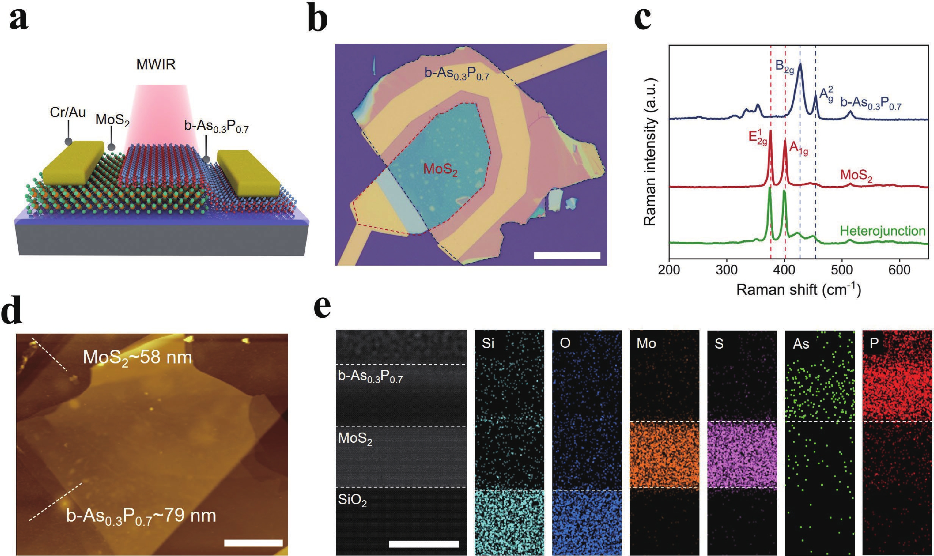
Fig. 1.  (Color online) Schematic diagram and characterizations of the b-As0.3P0.7/MoS2 heterojunction. (a) Schematic structural diagram of the b-As0.3P0.7/MoS2 heterojunction. (b) Optical image of the b-As0.3P0.7/MoS2 heterojunction. Scale bar: 25 μm. (c) Raman spectra of MoS2, b-As0.3P0.7, and the heterojunction region. (d) Thickness characterization of the b-As0.3P0.7/MoS2 heterojunction by AFM. Scale bar: 10 μm. (e) Cross-sectional STEM image and EDS mapping of the b-As0.3P0.7/MoS2 heterostructure, showing the spatial distributions of Si, O, Mo, S, As, and P elements. Scale bar: 25 nm.

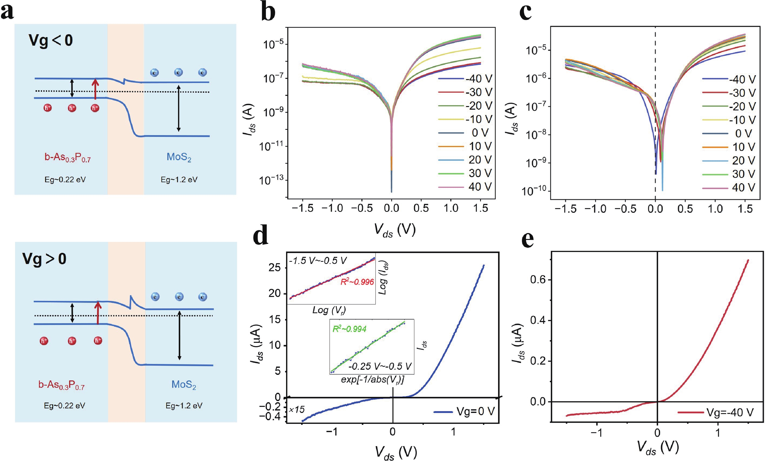
Fig. 2.  (Color online) Optoelectronic characteristics of the b-As0.3P0.7/MoS2 heterojunction at room temperature. (a) Schematic band diagrams of the b-As0.3P0.7/MoS2 heterojunction under positive and negative gate voltages. (b) Gate-dependent dark I-V characteristics as Vg increases from −40 V to 40 V. (c) Gate-dependent I-V characteristics under 520 nm laser illumination. (d) Dark I-V curve at Vg = 0 V and reverse-leakage fitting based on TAT and SCLC-like transport. (e) Dark I-V curve at Vg = −40 V.

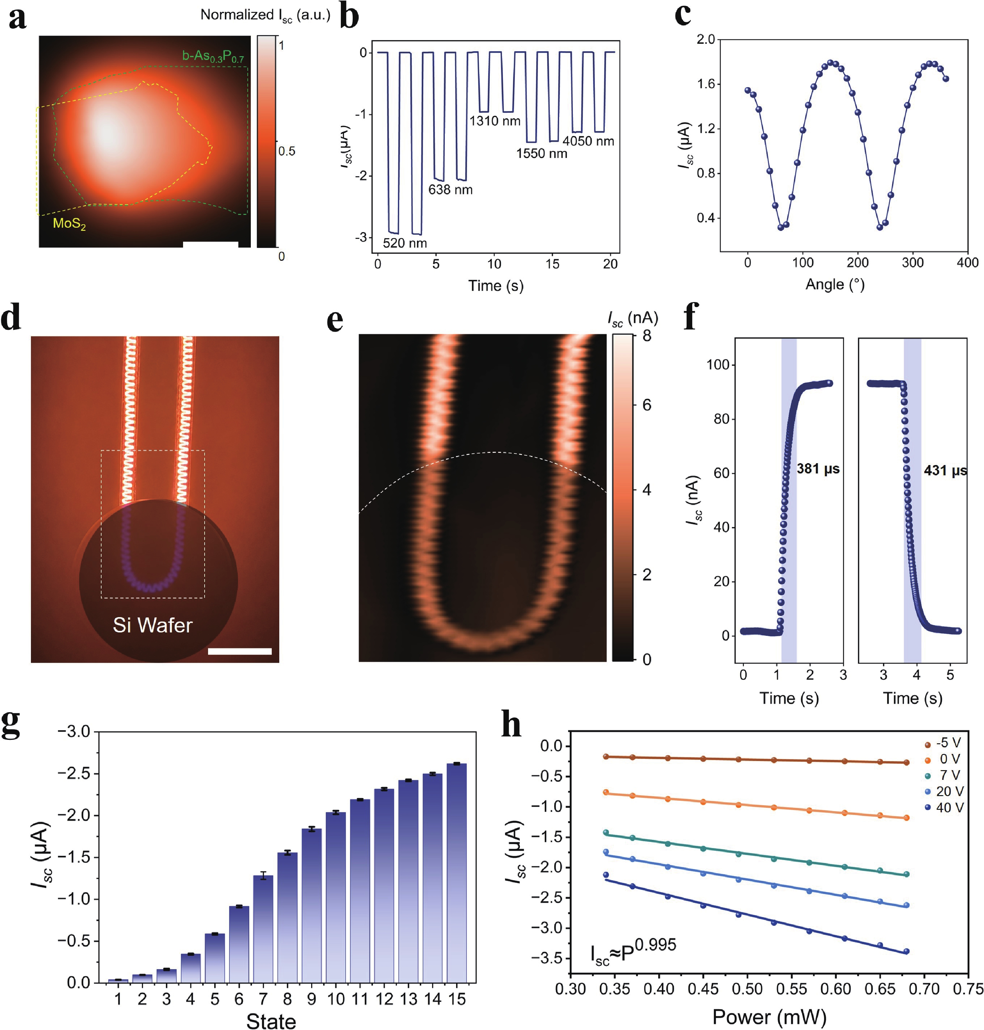
Fig. 3.  (Color online) Broadband and gate-reconfigurable infrared photoresponse of the b-As0.3P0.7/MoS2 heterojunction. (a) Scanning photocurrent microscope mapping measurement of the device under infrared illumination. Scale bar:25 μm. (b) Photo-response waveforms of the device over the visible-to-mid-wave-infrared range. (c) Polarization-dependent photocurrent under 1550 nm illumination, showing a polarization ratio of 5.64. (d) Optical photograph of the target consisting of a carbon-fiber heating tube covered by a silicon wafer. (e) Infrared image of the heated target behind the silicon wafer. (f) Time-resolved photoresponse under 1550 nm illumination. (g) Fifteen gate-programmed photoresponse states selected from the continuously gate-tunable response under 1550 nm illumination. States 1-15 correspond to Vg= −20, −15, −10, −5, 0, 2, 5, 7, 8, 10, 15, 20, 25, 30, and 40 V, respectively. The symbols and error bars represent the mean and one standard deviation of three repeated measurements, respectively. (h) Power-dependent short-circuit photocurrent under 1550 nm illumination, showing a power-law exponent of 0.995.

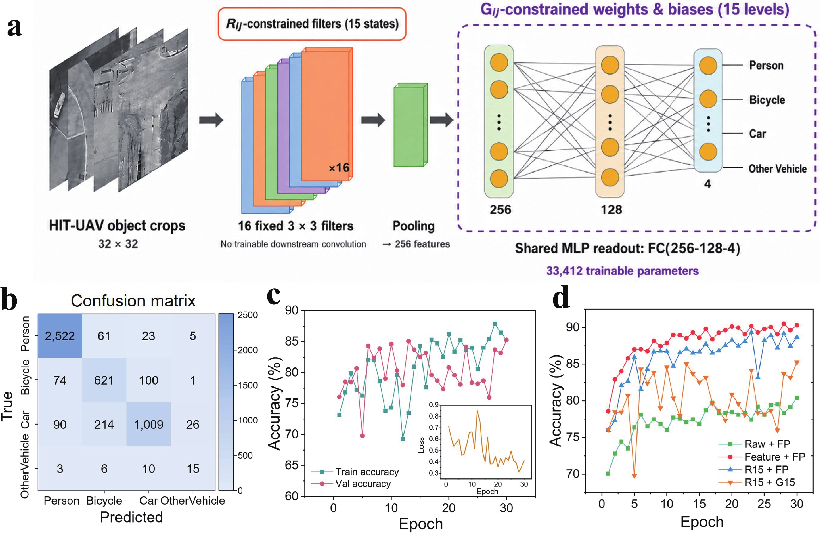
Fig. 4.  (Color online) Device-constrained simulation of HIT-UAV object classification. (a) Classification pipeline consisting of 16 fixed 3 × 3 filters, pooling to 256 features, and a neural network. The filters and network parameters are constrained to 15 Rij states and 15 Gij levels, respectively. (b) Test-set confusion matrix of scheme D for 4,780 object crops, with rows and columns representing the true and predicted classes. (c) Training and validation accuracies of scheme D, with the training loss shown in the inset. (d) Validation accuracies of the four schemes: raw-image inputs processed by a floating-point network (Raw + FP); floating-point image features processed by a floating-point classification network (Feature + FP); image features mapped to the 15 experimentally measured responsivity states and processed by a floating-point network (R15 + FP); and the same responsivity-mapped features processed by a network whose weights were quantized in simulation to 15 conductance levels (R15 + G15). Here, FP denotes floating-point computation, R15 denotes the 15 experimentally measured responsivity states, and G15 denotes the 15 discrete conductance levels used to represent the network weights in the device-constrained simulation.

[1]
Long M S, Gao A Y, Wang P, et al. Room temperature high-detectivity mid-infrared photodetectors based on black arsenic phosphorus. Sci Adv, 2017, 3(6): e1700589 doi: 10.1126/sciadv.1700589
[2]
Tang Q Y, Zhong F, Li Q, et al. Infrared photodetection from 2D/3D van der Waals heterostructures. Nanomaterials, 2023, 13(7): 1169 doi: 10.3390/nano13071169
[3]
Wang F K, Fang S, Zhang Y, et al. 2D computational photodetectors enabling multidimensional optical information perception. Nat Commun, 2025, 16: 6791 doi: 10.1038/s41467-025-61924-6
[4]
Wang F K, Hu F C, Dai M J, et al. A two-dimensional mid-infrared optoelectronic retina enabling simultaneous perception and encoding. Nat Commun, 2023, 14: 1938 doi: 10.1038/s41467-023-37623-5
[5]
Li T X, Miao J S, Fu X, et al. Reconfigurable, non-volatile neuromorphic photovoltaics. Nat Nanotechnol, 2023, 18(11): 1303 doi: 10.1038/s41565-023-01446-8
[6]
Fu X, Li T X, Cai B, et al. Graphene/MoS2–xOx/graphene photomemristor with tunable non-volatile responsivities for neuromorphic vision processing. Light Sci Appl, 2023, 12: 39 doi: 10.1038/s41377-023-01079-5
[7]
Xu H Y, Xie R Z, Miao J S, et al. Critical band-to-band-tunnelling based optoelectronic memory. Light Sci Appl, 2025, 14(1): 72 doi: 10.1038/s41377-025-01756-7
[8]
Liu B L, Köpf M, Abbas A N, et al. Black arsenic–phosphorus: layered anisotropic infrared semiconductors with highly tunable compositions and properties. Adv Mater, 2015, 27(30): 4423 doi: 10.1002/adma.201501758
[9]
Han R Y, Feng S, Sun D M, et al. Properties and photodetector applications of two-dimensional black arsenic phosphorus and black phosphorus. Sci China Inf Sci, 2021, 64(4): 140402 doi: 10.1007/s11432-020-3172-1
[10]
Shu Y Q, University S, et al. Two-Dimensionalblack arsenic phosphorusfor ultrafast photonics in near- and mid-infrared regimes. ACS Appl Mater Interfaces, 2020, 12(41): 46509 doi: 10.1021/acsami.0c12408
[11]
Liang J C, Hu Y, Zhang K Q, et al. 2D layered black arsenic-phosphorus materials: synthesis, properties, and device applications. Nano Res, 2022, 15(4): 3737
[12]
Zhang Z, Ji P R, Hu W B, et al. Gate-tunable flexible photodetector with wavelength-selective response based on asymmetric 2D heterostructures. Microsyst Nanoeng, 2025, 11: 243
[13]
Doan M H, Jin Y, Adhikari S, et al. Charge transport in MoS2/WSe2 van der Waals heterostructure with tunable inversion layer. ACS Nano, 2017, 11(4): 3832
[14]
Zhang Y, Wang F K, Wang Q J. Infrared optoelectronic logic gates and encrypted optical communication enabled by a b-AsP/MoTe2 heterostructure with bipolar photoresponse. Adv Funct Mater, 2026, 36(51): e32184
[15]
Karki B, Freelon B, Rajapakse M, et al. Strain-induced vibrational properties of few layer black phosphorus and MoTe2 via Raman spectroscopy. Nanotechnology, 2020, 31(42): 425707
[16]
Fei R, Yang L. Lattice vibrational modes and Raman scattering spectra of strained phosphorene. Appl Phys Lett, 2014, 105(8): 083120
[17]
Lin J T, Ho H S. Ge/GaAs heterostructure TFET with Schottky contact to suppress ambipolar and trap-assisted tunneling. IEEE Trans Electron Devices, 2023, 70(11): 6049
[18]
Le Corre V M, Duijnstee E A, El Tambouli O, et al. Revealing charge carrier mobility and defect densities in metal halide perovskites via space-charge-limited current measurements. ACS Energy Lett, 2021, 6(3): 1087
[19]
Huang G, Chen R S, Chen M X, et al. Transfer and beyond: emerging strategies and trends in two-dimensional material device fabrication. Chem Soc Rev, 2026, 55(5): 2574
[20]
Wang F K, Zhu S, Chen W D, et al. Multidimensional detection enabled by twisted black arsenic-phosphorus homojunctions. Nat Nanotechnol, 2024, 19(4): 455
[21]
Zhang S K, Jiao H X, Chen Y, et al. Multi-dimensional optical information acquisition based on a misaligned unipolar barrier photodetector. Nat Commun, 2024, 15: 7071
[22]
Han J Y, Fu Z Y, Wei J X, et al. 2D materials-based next-generation multidimensional photodetectors. Light Sci Appl, 2025, 14: 362
[23]
Chen J C, Xu X B, Chen C, et al. Stable b-AsP/InSe mid-infrared detector with high polarization-sensitivity for target feature discrimination. Adv Funct Mater, 2026, 36(24): e22145
[24]
Ju L, Zou B Q, Wang S F, et al. A polarization-sensitive photodetector based on a b-AsP/In2Se3 heterostructure. Nanoscale, 2025, 17: 25081-25089
[25]
Hua Y H, Tang L L, Xia C J, et al. Self-powered polarization-sensitive photodetector enabled by b-AsP/Ta2NiS5/PtSe2 van der Waals heterostructure. Adv Opt Mater, 2026, 14(11): e03232
[26]
Ha J, Ma Y S, An Y N, et al. Spectrally tunable 2D material-based infrared photodetectors for intelligent optoelectronics. Adv Funct Mater, 2026, 36(27): e19542
[27]
Hu X H, Du L, Qi C, et al. B-AsP as the saturable absorber for a mid-infrared 3 μm nanosecond laser. Opt Continuum, 2024, 3(12): 2314

supplementary_material.pdf

  • Search

    Advanced Search >>

    GET CITATION

    shu

    Export: BibTex EndNote

    Article Metrics

    Article views: 4 Times PDF downloads: 1 Times Cited by: 0 Times

    History

    Received: 15 June 2026 Revised: 16 August 2026 Online: Accepted Manuscript: 23 September 2026

    Catalog

      Email This Article

      User name:
      Email:*请输入正确邮箱
      Code:*验证码错误
      Yuelin Zhang, Tangxin Li, Yuxuan Pei, Ziyue Song, Hangyu Xu, Xiao Fu, Mingkai Li, Min Luo. Broadband gate-reconfigurable infrared sensing based on a b-As0.3P0.7/MoS2 heterojunction[J]. Journal of Semiconductors, 2026, In Press. doi: 10.1088/1674-4926/26060028 ****Y L Zhang, T X Li, Y X Pei, Z Y Song, H Y Xu, X Fu, M K Li, and M Luo, Broadband gate-reconfigurable infrared sensing based on a b-As0.3P0.7/MoS2 heterojunction[J]. J. Semicond., 2026, accepted doi: 10.1088/1674-4926/26060028
      Citation:
      Yuelin Zhang, Tangxin Li, Yuxuan Pei, Ziyue Song, Hangyu Xu, Xiao Fu, Mingkai Li, Min Luo. Broadband gate-reconfigurable infrared sensing based on a b-As0.3P0.7/MoS2 heterojunction[J]. Journal of Semiconductors, 2026, In Press. doi: 10.1088/1674-4926/26060028 ****
      Y L Zhang, T X Li, Y X Pei, Z Y Song, H Y Xu, X Fu, M K Li, and M Luo, Broadband gate-reconfigurable infrared sensing based on a b-As0.3P0.7/MoS2 heterojunction[J]. J. Semicond., 2026, accepted doi: 10.1088/1674-4926/26060028

      Broadband gate-reconfigurable infrared sensing based on a b-As0.3P0.7/MoS2 heterojunction

      DOI: 10.1088/1674-4926/26060028
      CSTR: 32376.14.1674-4926.26060028
      More Information
      • Yuelin Zhang received the B.S. degree from China Three Gorges University in 2023. She is currently pursuing the M.S. degree at Hubei University, China. Her current research interests include two-dimensional optoelectronic devices, infrared photodetectors, and high-dimensional optoelectronic sensing
      • Mingkai Li received the B.S. degree and the Ph.D. degree in physics from Wuhan University, China, in 1998 and 2004, respectively. From 2004 to 2011, he worked at the Quantum-Functional Semiconductor Research Center, Dongguk University, South Korea. He is currently a Professor with the School of Materials Science and Engineering, Hubei University, China. His current research interests include ultrawide-bandgap semiconductor materials, solar-blind ultraviolet photodetectors, and novel semiconductor devices
      • Min Luo received her doctoral degree from Chinese Academy of Sciences, in 2026. She is currently an assistant Professor with the Shanghai Institute of Technical Physics of the Chinese Academy of Sciences, Shanghai, China. Her current research interests include light-matter interactions in infrared detectors and computational devices, as well as the underlying physics
      • Corresponding author: mkli@hubu.edu.cnluomin17@mails.ucas.ac.cn
      • Received Date: 2026-06-15
      • Revised Date: 2026-08-16
      • Available Online: 2026-09-23

      Catalog

        /

        DownLoad:  Full-Size Img  PowerPoint
        Return
        Return