J. Semicond. >  Just Accepted

REVIEWS

Low-dimensional perovskite optoelectronic synapses for neuromorphic vision

Zhihao Xu1, 4, §, Yingjie Luo2, §, Alson Yau3, §, Yuan Meng1, Seung-il Kim1, Kyubeen Kim1, Sheng Ran2 and Sang-Hoon Bae1, 4,

+ Author Affiliations

 Corresponding author: Sang-Hoon Bae, sbae22@wustl.edu

DOI: 10.1088/1674-4926/26060035CSTR: 32376.14.1674-4926.26060035

PDF

Turn off MathJax

Abstract: Low-dimensional metal-halide perovskites have emerged as promising materials for optoelectronic synapses and neuromorphic vision systems owing to their strong light–matter interactions, tunable optoelectronic properties, and mixed ionic–electronic transport. Compared with three-dimensional counterparts, low-dimensional perovskites exhibit more powerful control over charge transport, ion migration, and optical absorption with enhanced stability. In this review, we outline the composition, dimensionality, and growth strategies of low-dimensional perovskites, emphasizing how structural engineering governs their optical and electrical properties. Their photodetection, memristive, and photo-reservoir behaviors are further discussed to form physical foundation for light-stimulated synaptic functions, including optical sensing, memory retention, and conductance modulation. We review representative optoelectronic synapses based on 0D, 1D, and 2D perovskites according to their device-level mechanisms, highlighting how dimensionality enables distinct visual functions and device architectures. Exemplary neuromorphic algorithms are discussed as well, including artificial neural networks, convolutional neural networks, spiking neural networks, recurrent neural networks, and reservoir computing, which translate perovskite synaptic responses into higher-level capabilities such as image recognition, multimodal perception, and motion detection. Finally, we catalog the remaining challenges including lead toxicity, limited lead-free performance, crystallization and device-to-device variations, ion-migration-induced instability, and options for wafer-scale patterning and addressable integration. By connecting materials design, synaptic device physics, neuromorphic algorithms, and scalable integration strategies, with perspectives on how low-dimensional perovskites can evolve from laboratory-scale optoelectronic synapses into practical platforms for next-generation artificial vision systems.


[1]
Horowitz M. 1.1 computing’s energy problem (and what we can do about it). 2014 IEEE International Solid-State Circuits Conference Digest of Technical Papers (ISSCC), 2014: 10
[2]
Ding G L, Li H, Zhao J Y, et al. Nanomaterials for flexible neuromorphics. Chem Rev, 2024, 124(22): 12738 doi: 10.1021/acs.chemrev.4c00369
[3]
Ding G L, Zhao J Y, Zhou K, et al. Porous crystalline materials for memories and neuromorphic computing systems. Chem Soc Rev, 2023, 52(20): 7071 doi: 10.1039/D3CS00259D
[4]
Chang Y, Na S Y, Ro Y G, et al. Robust biodegradable synapse with sub-biological energy and extended memory for intelligent reflexive system. Nat Commun, 2025, 16: 10610 doi: 10.1038/s41467-025-66511-3
[5]
Zhang H, Ye J Y, Gao M B, et al. Single-molecule neuromorphic device with aJ-level power consumption per switching. Nat Commun, 2026, 17: 4655 doi: 10.1038/s41467-026-71127-2
[6]
Guo L Q, Sun H X, Min L L, et al. Two-terminal perovskite optoelectronic synapse for rapid trained neuromorphic computation with high accuracy. Adv Mater, 2024, 36(27): 2402253 doi: 10.1002/adma.202402253
[7]
Kim H, Choi M J, Suh J M, et al. Quasi-2D halide perovskites for resistive switching devices with ON/OFF ratios above 109. NPG Asia Mater, 2020, 12: 21 doi: 10.1038/s41427-020-0202-2
[8]
Zhang Y T, Poddar S, Huang H, et al. Three-dimensional perovskite nanowire array–based ultrafast resistive RAM with ultralong data retention. Sci Adv, 2021, 7(36): eabg3788 doi: 10.1126/sciadv.abg3788
[9]
XITONG HONG X L. Review on metal halide perovskite-based optoelectronic synapses. Photonics Res, 2023, 11(5): 787
[10]
Guan X W, Lei Z H, Yu X C, et al. Low-dimensional metal-halide perovskites as high-performance materials for memory applications. Small, 2022, 18(38): 2203311 doi: 10.1002/smll.202203311
[11]
Rafique H, Abbas G, Mendes M J, et al. Recent advancements and perspectives of low-dimensional halide perovskites for visual perception and optoelectronic applications. Nano Micro Lett, 2025, 18(1): 44
[12]
Kim S I, Lee Y, Park M H, et al. Dimensionality dependent plasticity in halide perovskite artificial synapses for neuromorphic computing. Adv Electron Mater, 2019, 5(9): 1900008 doi: 10.1002/aelm.201900008
[13]
Im J H, Luo J S, Franckevičius M, et al. Nanowire perovskite solar cell. Nano Lett, 2015, 15(3): 2120 doi: 10.1021/acs.nanolett.5b00046
[14]
Spina M, Bonvin E, Sienkiewicz A, et al. Controlled growth of CH3NH3PbI3 nanowires in arrays of open nanofluidic channels. Sci Rep, 2016, 6: 19834 doi: 10.1038/srep19834
[15]
Zhang J, Yang X K, Deng H, et al. Low-dimensional halide perovskites and their advanced optoelectronic applications. Nano Micro Lett, 2017, 9(3): 36 doi: 10.1007/s40820-017-0137-5
[16]
Zhu Z H, Zhu C, Yang L, et al. Room-temperature epitaxial welding of 3D and 2D perovskites. Nat Mater, 2022, 21(9): 1042 doi: 10.1038/s41563-022-01311-4
[17]
Liu J Q, Gong J D, Wei H H, et al. A bioinspired flexible neuromuscular system based thermal-annealing-free perovskite with passivation. Nat Commun, 2022, 13: 7427 doi: 10.1038/s41467-022-35092-w
[18]
Zhou L E, Han S Y, Liu H, et al. Energy-efficient, stable, and temperature-tolerant neuromorphic device based on single crystals of halide perovskites. Cell Rep Phys Sci, 2024, 5(7): 102078 doi: 10.1016/j.xcrp.2024.102078
[19]
Babayigit A, Ethirajan A, Muller M, et al. Toxicity of organometal halide perovskite solar cells. Nat Mater, 2016, 15(3): 247 doi: 10.1038/nmat4572
[20]
Zhou Y Y, Zhao Y X. Chemical stability and instability of inorganic halide perovskites. Energy Environ Sci, 2019, 12(5): 1495 doi: 10.1039/C8EE03559H
[21]
Wang Y, Lv Z Y, Chen J R, et al. Photonic synapses based on inorganic perovskite quantum dots for neuromorphic computing. Adv Mater, 2018, 30(38): 1802883 doi: 10.1002/adma.201802883
[22]
Vishwanath S K, Karkera C, et al. Lead-free Cs3Bi2I9Perovskite memristors for energy-efficient neuromorphic computing. ACS Energy Lett, 2025, 10(5): 2193 doi: 10.1021/acsenergylett.5c00411
[23]
Du Y J, Yang J J, Lv Z Y, et al. Integration of perovskite/low-dimensional material heterostructures for optoelectronics and artificial visual systems. Adv Funct Mater, 2025, 35(36): 2500953 doi: 10.1002/adfm.202500953
[24]
Lin Y, Bai Y, Fang Y J, et al. Suppressed ion migration in low-dimensional perovskites. ACS Energy Lett, 2017, 2(7): 1571 doi: 10.1021/acsenergylett.7b00442
[25]
Meng Y, Zhong H K, Xu Z H, et al. Functionalizing nanophotonic structures with 2D van der Waals materials. Nanoscale Horiz, 2023, 8(10): 1345 doi: 10.1039/D3NH00246B
[26]
Yang P, Yu X P, Yu R J, et al. High polarization-sensitive synaptic transistor based on perovskite nanowire array for efficient biometric recognition. Adv Funct Mater, 2025, 35(11): 2416954 doi: 10.1002/adfm.202416954
[27]
Ghimire S, Klinke C. Two-dimensional halide perovskites: Synthesis, optoelectronic properties, stability, and applications. Nanoscale, 2021, 13(29): 12394 doi: 10.1039/D1NR02769G
[28]
Xia Y N, Yang P D, Sun Y G, et al. One-dimensional nanostructures: Synthesis, characterization, and applications. ChemInform, 2003, 34(22): 200322236 doi: 10.1002/chin.200322236
[29]
Pradhan B, Das S, Li J X, et al. Ultrasensitive and ultrathin phototransistors and photonic synapses using perovskite quantum dots grown from graphene lattice. Sci Adv, 2020, 6(7): eaay5225 doi: 10.1126/sciadv.aay5225
[30]
Long Z H, Qiu X, Chan C L J, et al. A neuromorphic bionic eye with filter-free color vision using hemispherical perovskite nanowire array retina. Nat Commun, 2023, 14: 1972 doi: 10.1038/s41467-023-37581-y
[31]
Liu Q, Wei Q, Ren H, et al. Circular polarization-resolved ultraviolet photonic artificial synapse based on chiral perovskite. Nat Commun, 2023, 14: 7179 doi: 10.1038/s41467-023-43034-3
[32]
Bao C X, Yang J, Bai S, et al. High performance and stable all-inorganic metal halide perovskite-based photodetectors for optical communication applications. Adv Mater, 2018, 30(38): 1803422 doi: 10.1002/adma.201803422
[33]
Wang H P, Li S Y, Liu X Y, et al. Low-dimensional metal halide perovskite photodetectors. Adv Mater, 2021, 33(7): 2003309 doi: 10.1002/adma.202003309
[34]
Feng J G, Gong C, Gao H F, et al. Single-crystalline layered metal-halide perovskite nanowires for ultrasensitive photodetectors. Nat Electron, 2018, 1(7): 404 doi: 10.1038/s41928-018-0101-5
[35]
Zhu H M, Fu Y P, Meng F, et al. Lead halide perovskite nanowire lasers with low lasing thresholds and high quality factors. Nat Mater, 2015, 14(6): 636 doi: 10.1038/nmat4271
[36]
Vasilopoulou M, bin Mohd Yusoff A R, Chai Y, et al. Neuromorphic computing based on halide perovskites. Nat Electron, 2023, 6(12): 949 doi: 10.1038/s41928-023-01082-z
[37]
John R A, Demirağ Y, Shynkarenko Y, et al. Reconfigurable halide perovskite nanocrystal memristors for neuromorphic computing. Nat Commun, 2022, 13: 2074 doi: 10.1038/s41467-022-29727-1
[38]
Kim S J, Im I H, Baek J H, et al. Linearly programmable two-dimensional halide perovskite memristor arrays for neuromorphic computing. Nat Nanotechnol, 2025, 20(1): 83 doi: 10.1038/s41565-024-01790-3
[39]
Gao S, Liu G, Yang H L, et al. An oxide Schottky junction artificial optoelectronic synapse. ACS Nano, 2019, 13(2): 2634 doi: 10.1021/acsnano.9b00340
[40]
Liu K Q, Zhang T, Dang B J, et al. An optoelectronic synapse based on α-In2Se3 with controllable temporal dynamics for multimode and multiscale reservoir computing. Nat Electron, 2022, 5(11): 761 doi: 10.1038/s41928-022-00847-2
[41]
Xu H Y, Xu Z H, Ren Q Q, et al. Two-dimensional materials for integrated sensing. Nat Mater, 2026: 1
[42]
Yang Z Y, Huo S D, Zhang Z, et al. High-precision multibit opto-electronic synapses based on ReS2/h-BN/graphene heterostructure for energy-efficient and high-accuracy neuromorphic computing. Adv Funct Mater, 2025, 35(48): 2509119 doi: 10.1002/adfm.202509119
[43]
Zhou F C, Chai Y. Near-sensor and in-sensor computing. Nat Electron, 2020, 3(11): 664 doi: 10.1038/s41928-020-00501-9
[44]
Huang C Y, Li H C, Wu Y, et al. Inorganic halide perovskite quantum dots: A versatile nanomaterial platform for electronic applications. Nano Micro Lett, 2022, 15(1): 16
[45]
Cheng Y C, Li H, Liu B, et al. Vertical 0D-perovskite/2D-MoS2 van der Waals heterojunction phototransistor for emulating photoelectric-synergistically classical Pavlovian conditioning and neural coding dynamics. Small, 2020, 16(45): 2005217 doi: 10.1002/smll.202005217
[46]
Li J X, Dwivedi P, Kumar K S, et al. Growing perovskite quantum dots on carbon nanotubes for neuromorphic optoelectronic computing. Adv Electron Mater, 2021, 7(1): 2000535 doi: 10.1002/aelm.202000535
[47]
Meng Y, Feng J G, Han S, et al. Photonic van der Waals integration from 2D materials to 3D nanomembranes. Nat Rev Mater, 2023, 8(8): 498 doi: 10.1038/s41578-023-00558-w
[48]
Gu L L, Poddar S, Lin Y J, et al. A biomimetic eye with a hemispherical perovskite nanowire array retina. Nature, 2020, 581(7808): 278 doi: 10.1038/s41586-020-2285-x
[49]
Zhou Y, Sun Z B, Ding Y C, et al. An ultrawide field-of-view pinhole compound eye using hemispherical nanowire array for robot vision. Sci Robot, 2024, 9(90): eadi8666 doi: 10.1126/scirobotics.adi8666
[50]
Ren W, Zhao X M, Tang J, et al. A self-powered spherical compound eye with 8 ns-motion response for source-constrained drones. Nat Commun, 2026, 17: 6864 doi: 10.1038/s41467-026-73745-2
[51]
Liu Q, Wang P Z, Wei Q, et al. Chiral perovskite nanowire optoelectronic synapse for full-stokes polarization-resolved perception and reservoir computing. Adv Funct Mater, 2025, 35(8): 2415551 doi: 10.1002/adfm.202415551
[52]
Wang Y, Lei J C, Wang X, et al. Tear-film-inspired moisture-resistant and mechanical flexible perovskite microwire artificial visual system. Laser Photonics Rev, 2026, 20(13): e03181 doi: 10.1002/lpor.202503181
[53]
Ma F M, Zhu Y B, Xu Z W, et al. Optoelectronic perovskite synapses for neuromorphic computing. Adv Funct Mater, 2020, 30(11): 1908901 doi: 10.1002/adfm.201908901
[54]
Hong X T, Huang Y L, Tian Q L, et al. Two-dimensional perovskite-gated AlGaN/GaN high-electron-mobility-transistor for neuromorphic vision sensor. Adv Sci, 2022, 9(27): 2202019 doi: 10.1002/advs.202202019
[55]
Li Y T, Li J Z, Ren L, et al. Light-controlled reconfigurable optical synapse based on carbon nanotubes/2D perovskite heterostructure for image recognition. ACS Appl Mater Interfaces, 2022, 14(24): 28221 doi: 10.1021/acsami.2c05818
[56]
Gong J D, Wei H H, Liu J Q, et al. An artificial visual nerve for mimicking pupil reflex. Matter, 2022, 5(5): 1578 doi: 10.1016/j.matt.2022.02.020
[57]
Liu F, Zhang X Y, Valencia A, et al. Low energy consumption and stable perovskite-based photonic synapse with two-terminal lateral configuration. Nano Energy, 2025, 142: 111145 doi: 10.1016/j.nanoen.2025.111145
[58]
Sahu D, Nandi S J, et al. Ultralow energy optoelectronic synapse using halide perovskite/organic semiconductor heterostructure for neuromorphic computing, optical logic and wireless communication. ACS Appl Mater Interfaces, 2026, 18(18): 26509 doi: 10.1021/acsami.6c03922
[59]
Dan S, Paramanik S, Pal A J. Introducing chiro-optical activities in photonic synapses for neuromorphic computing and in-memory logic operations. ACS Nano, 2024, 18(22): 14457 doi: 10.1021/acsnano.4c01202
[60]
Zhou X, Hu F Z, Hou Q, et al. All-photonic artificial synapses based on photochromic perovskites for noncontact neuromorphic visual perception. Commun Mater, 2024, 5: 116 doi: 10.1038/s43246-024-00553-w
[61]
Liu Y, Wang B, Wu L, et al. Artificial visual synaptic architecture with high-linearity light-modulated weight for optoelectronic neuromorphic computing. ACS Appl Mater Interfaces, 2023, 15(44): 51380 doi: 10.1021/acsami.3c11495
[62]
Xia J N, Gao C S, Peng C Y, et al. Multidimensional deep ultraviolet (DUV) synapses based on organic/perovskite semiconductor heterojunction transistors for antispoofing facial recognition systems. Nano Lett, 2024, 24(22): 6673 doi: 10.1021/acs.nanolett.4c01356
[63]
Xie C, University A, Li C, et al. Electron trapping enhanced deep-ultraviolet optoelectronic synapses based on two-dimensional wide-bandgap perovskite/organic-semiconductor heterojunctions. Nano Lett, 2025, 25(40): 14686 doi: 10.1021/acs.nanolett.5c03851
[64]
Cui D S, University X, et al. Self-powered halide perovskite optoelectronic synaptic memristors for reconfigurable logic and reservoir computing applications. Nano Lett, 2025, 25(43): 15705 doi: 10.1021/acs.nanolett.5c04297
[65]
Huang W, Tang J W, Li B, et al. Design of all-optical bidirectional self-powered synaptic devices for neuromorphic computing applications. Small, 2025, 21(34): 2505327 doi: 10.1002/smll.202505327
[66]
Yang X Y, Xiong Z Y, Chen Y J, et al. A self-powered artificial retina perception system for image preprocessing based on photovoltaic devices and memristive arrays. Nano Energy, 2020, 78: 105246 doi: 10.1016/j.nanoen.2020.105246
[67]
Lin Q H, Zhu Y B, Hu X, et al. Multifunctional PN optoelectronic synapse and its smart integration towards augmented artificial visual system. npj Flex Electron, 2025, 9: 81 doi: 10.1038/s41528-025-00459-8
[68]
Shao H, Li Y Q, Yang W, et al. A reconfigurable optoelectronic synaptic transistor with stable Zr-CsPbI3 nanocrystals for visuomorphic computing. Adv Mater, 2023, 35(12): 2208497 doi: 10.1002/adma.202208497
[69]
Poddar S, Khan B, Kumar S, et al. Ultra-high density perovskite nanowire array memristor-based multi-layer perceptron. Nat Commun, 2026, 17: 5576 doi: 10.1038/s41467-026-71372-5
[70]
Miao J S, Song B, Xu Z H, et al. Single pixel black phosphorus photodetector for near-infrared imaging. Small, 2018, 14(2): 1702082 doi: 10.1002/smll.201702082
[71]
Zhou Y, Fu J W, Chen Z R, et al. Computational event-driven vision sensors for in-sensor spiking neural networks. Nat Electron, 2023, 6(11): 870 doi: 10.1038/s41928-023-01055-2
[72]
Chien Y C, Xiang H, Shi Y F, et al. A MoS2 hafnium oxide based ferroelectric encoder for temporal-efficient spiking neural network. Adv Mater, 2023, 35(2): 2204949 doi: 10.1002/adma.202204949
[73]
Liu S X, Wu Z X, He Z L, et al. Low-power perovskite neuromorphic synapse with enhanced photon efficiency for directional motion perception. ACS Appl Mater Interfaces, 2024, 16(17): 22303 doi: 10.1021/acsami.4c04398
[74]
Zi J Z, Sun J, Yang B, et al. Multidimensional and reconfigurable optical neuromorphic computing using perovskite-based all-photonic synapses. Commun Mater, 2026, 7: 92 doi: 10.1038/s43246-026-01097-x
[75]
Wang H, Lin R Y, Zhao K B, et al. Dual-way alternation sensing memristors based on (BA)2(MA)3Pb4Br13 ferroelectric quantum dots with sub-0.16 V switching for broadband image-recognition systems. Adv Funct Mater, 2025, 35(46): 2510543 doi: 10.1002/adfm.202510543
[76]
Liu S J, Cheng Z P, Li M Y, et al. Synapses based on lead-free perovskite in artificial intelligence. Matter, 2024, 7(9): 2810
[77]
Li M C, Li C, Ye K, et al. Self-powered photonic synapses with rapid optical erasing ability for neuromorphic visual perception. Research, 2024, 7: 526
[78]
Harwell J, Burch J, Fikouras A, et al. Patterning multicolor hybrid perovskite FilmsviaTop-down lithography. ACS Nano, 2019, 13(4): 3823
[79]
Wang G M, Li D H, Cheng H C, et al. Wafer-scale growth of large arrays of perovskite microplate crystals for functional electronics and optoelectronics. Sci Adv, 2015, 1(9): e1500613
[80]
Wang R, Wang J T, Tan S, et al. Opportunities and challenges of lead-free perovskite optoelectronic devices. Trends Chem, 2019, 1(4): 368
[81]
Wang M, Wang W, Ma B, et al. Lead-Free Perovskite Materials for Solar Cells. Nano-Micro Letters, 2021, 13(1), 62 [81] Wang M H, Wang W, Ma B, et al. Lead-free perovskite materials for solar cells. Nano Micro Lett, 2021, 13(1): 62
[82]
Zhang Y Q, Ma Y, Wang Y X, et al. Lead-free perovskite photodetectors: Progress, challenges, and opportunities. Adv Mater, 2021, 33(26): 2006691
[83]
Kwak K J, Baek J H, Lee D E, et al. Ambient stable all inorganic CsCu2I3 artificial synapses for neurocomputing. Nano Lett, 2022, 22(14): 6010
[84]
Zheng Y Q, Xu H Y, Xu H, et al. Twelve-inch electrically anisotropic boridene for optoelectronic computing. Nat Nanotechnol, 2026, 21(4): 571
[85]
Zhang Z, Tian Q J, Huo S D, et al. Photodoping strategies in two-dimensional semiconductors: Mechanisms, characterizations, and emerging applications. InfoMat, 2025, 7(12): e70092
[86]
Jeong B, Han H, Park C. Micro- and nanopatterning of halide perovskites where crystal engineering for emerging photoelectronics meets integrated device array technology. Adv Mater, 2020, 32(30): 2000597
[87]
Wang K Y, Xing G C, Song Q H, et al. Micro- and nanostructured lead halide perovskites: From materials to integrations and devices. Adv Mater, 2021, 33(6): 2000306
[88]
Xu Z H, Chin S H, Park B I, et al. Advancing perovskite solar cell commercialization: Bridging materials, vacuum deposition, and AI-assisted automation. Next Mater, 2024, 3: 100103
[89]
Liang L M, Ma T, Chen Z Y, et al. Patterning technologies for metal halide perovskites: A review. Adv Mater Technol, 2023, 8(3): 2200419
[90]
Lyashenko D, Perez A, Zakhidov A. High-resolution patterning of organohalide lead perovskite pixels for photodetectors using orthogonal photolithography. Phys Status Solidi A, 2017, 214(1): 1600302
[91]
Cegielski P J, Giesecke A L, Neutzner S, et al. Monolithically integrated perovskite SemiconductorLasers on silicon photonic chips by scalable top-down fabrication. Nano Lett, 2018, 18(11): 6915
[92]
Gu Z K, Wang K, Li H Z, et al. Direct-writing multifunctional perovskite single crystal arrays by inkjet printing. Small, 2017, 13(8): 1603217
[93]
Chou S S, Swartzentruber B S, Foley-Janish M T, et al. Laser direct write synthesis of lead halide perovskites. J Phys Chem Lett, 2016, 7(19): 3736
[94]
Zhizhchenko A, Syubaev S, Berestennikov A, et al. Single-mode lasing from imprinted halide-perovskite microdisks. ACS Nano, 2019, 13(4): 4140
[95]
Niu L, Liu X F, Cong C X, et al. Controlled synthesis of organic/inorganic van der Waals solid for tunable light–matter interactions. Adv Mater, 2015, 27(47): 7800
[96]
Wu E X, Wang Y, Huo S D, et al. Universal core–shell nanowire memristor platform with quasi-2D filament confinement for scalable neuromorphic applications. Adv Funct Mater, 2026, 36(11): e18764
[97]
Liu Y, Huang Y, Duan X F. Van der Waals integration before and beyond two-dimensional materials. Nature, 2019, 567(7748): 323
[98]
Kum H S, Lee H, Kim S, et al. Heterogeneous integration of single-crystalline complex-oxide membranes. Nature, 2020, 578(7793): 75
[99]
Meng Y, Mao W, Xu Z, et al. Heterogeneous photonic integration of single-crystalline nanomembranes. Research Square Preprint, 2025, DOI: 10.1038/s41586-026-11000-w
[100]
Kaur P, Boes A, Ren G H, et al. Hybrid and heterogeneous photonic integration. APL Photonics, 2021, 6(6): 061102
[101]
Pintus P, Dumont M, Shah V, et al. Integrated non-reciprocal magneto-optics with ultra-high endurance for photonic in-memory computing. Nat Photonics, 2025, 19(1): 54
[102]
Geler-Kremer J, Eltes F, Stark P, et al. A ferroelectric multilevel non-volatile photonic phase shifter. Nat Photonics, 2022, 16(7): 491
[103]
Xu H Y, Xie R Z, Miao J S, et al. Critical band-to-band-tunnelling based optoelectronic memory. Light Sci Appl, 2025, 14: 72
[104]
Kang J H, Shin H, Kim K S, et al. Monolithic 3D integration of 2D materials-based electronics towards ultimate edge computing solutions. Nat Mater, 2023, 22(12): 1470
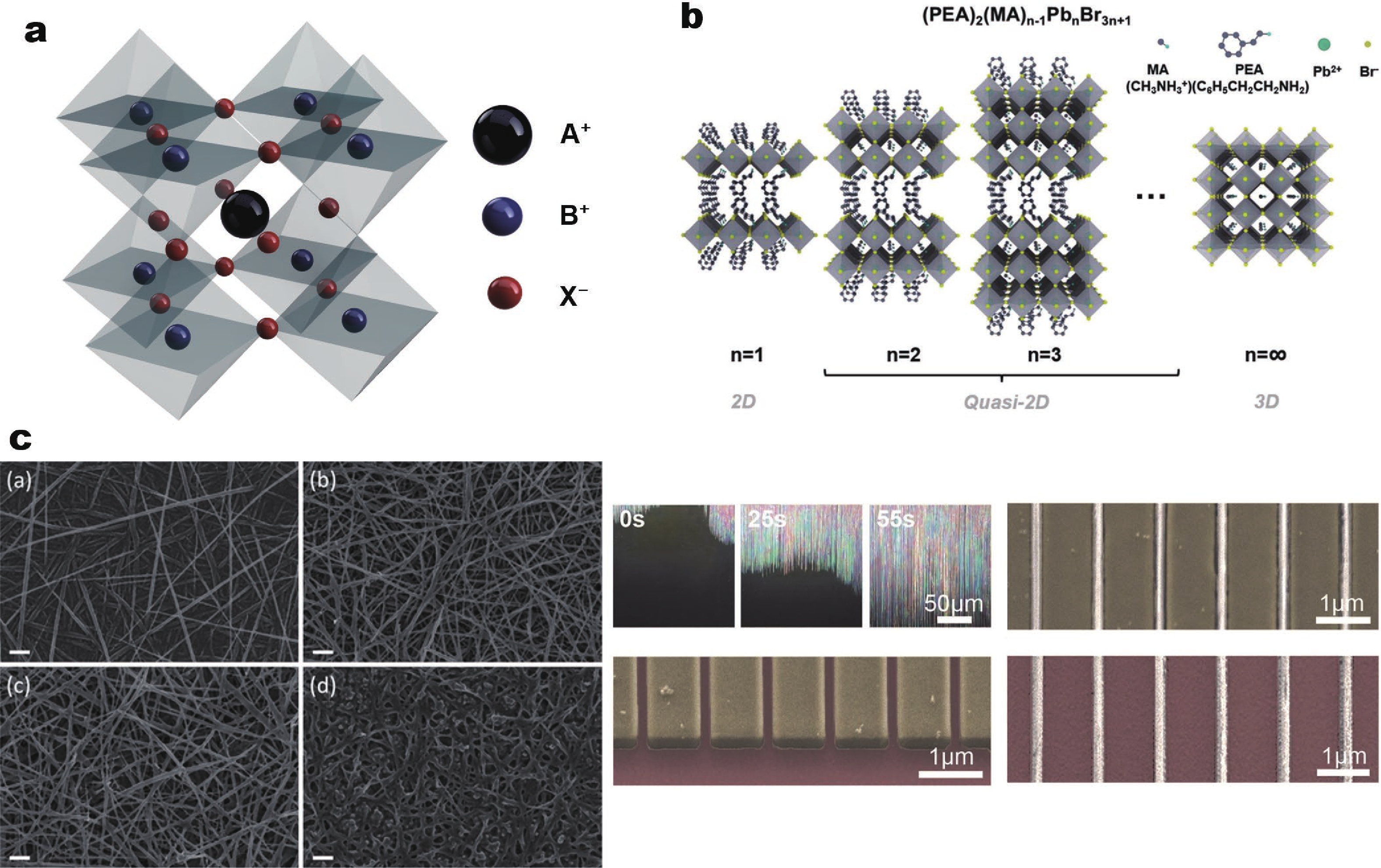
Fig. 1.  (Color online) Composition, dimensionality, and patterning strategies of metal halide perovskites. (a) Schematic crystal structure of a three-dimensional metal halide perovskite with formula AMX3. (b) Representative of the dimensional evolution of perovskite from 2D to 3D structures[12]. Adapted from Kim et al., Advanced Electronic Materials, 2019 (c) Comparison of representative MAPbI3 nanowire growth strategies. Spin coating produces interconnected nanowire networks with morphology dependent on growth conditions, whereas nanofluidic-channel templating guides crystallization into spatially defined nanowire arrays[13, 14]. Adapted from Im et al., Nano Letters, 2015 and Spina et al., Scientific Reports, 2016.

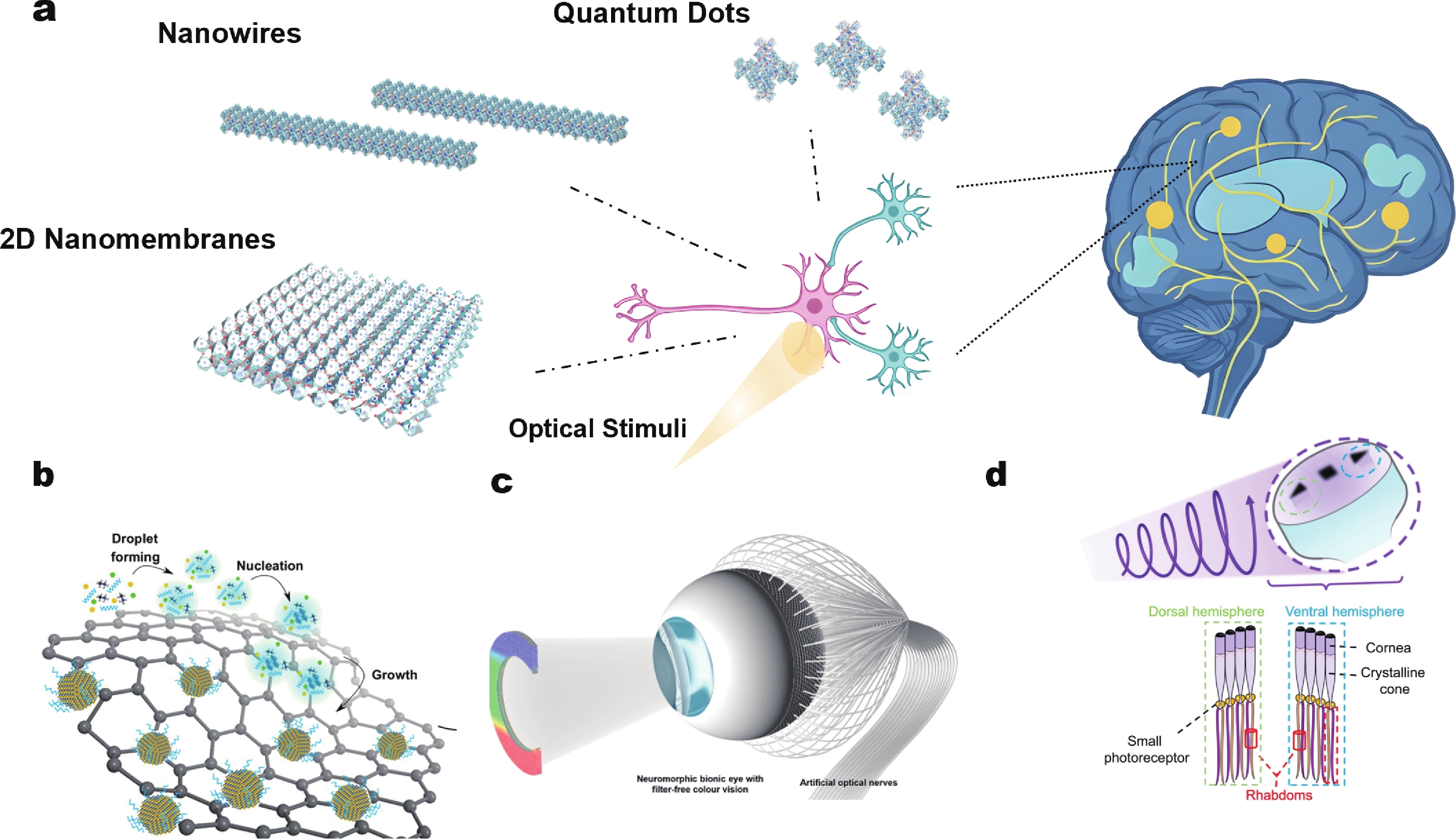
Fig. 2.  (Color online) Artificial vision systems using LDPs. (a) Schematic of perovskite quantum dots, nanowires, and 2D nanomembranes and artificial optical neurons. (b) Schematic showing the growth of perovskite quantum dots directly on graphene, presenting a hybrid optoelectronic synapse[29]. Reproduced from Pradhan et al., Science Advances, 2020. (c) The overall structure of a neuromorphic bionic eye based on hemispherical perovskite nanowire arrays with filter-free color vision[30]. Reproduced from Long et al., Nature Communications, 2023. (d) Schematic diagram of circular polarization-sensitive system based on perovskite nanomembranes and carbon nanotubes heterojunctions[31]. Adapted from Liu et al., Nature Communications, 2023.

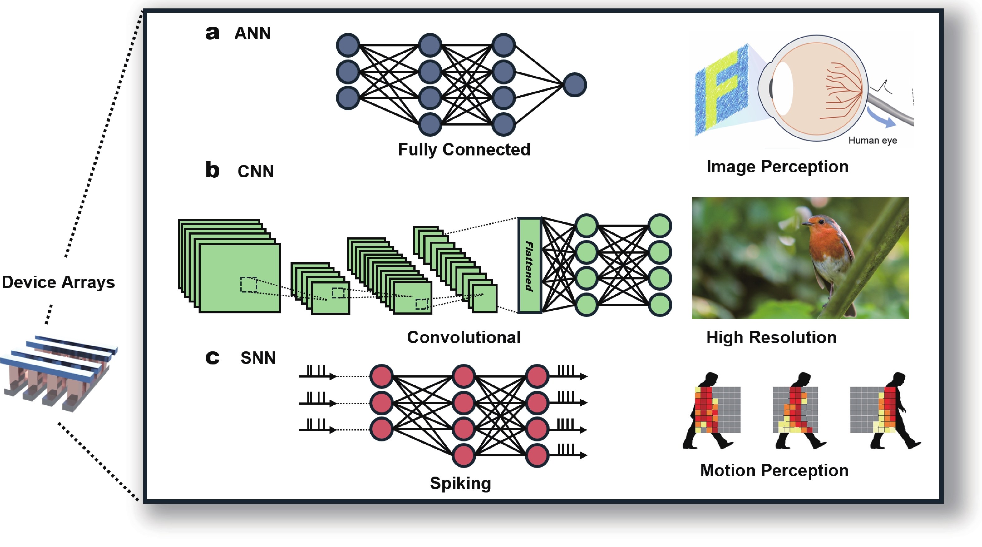
Fig. 3.  (Color online) Representative artificial neural networks and use cases. (a) Conventional Artificial Neural Networks using fully-connected layers for vision perception and classification[67]. Adapted from Lin et al., npj Flexible Electronics, 2025. (b) Convolutional Neural Network architectures for extracting spatial image features, enabling high-resolution visual recognition. (c) Spiking Neural Network architectures using spike-based signal transmission for dynamic and motion perception.

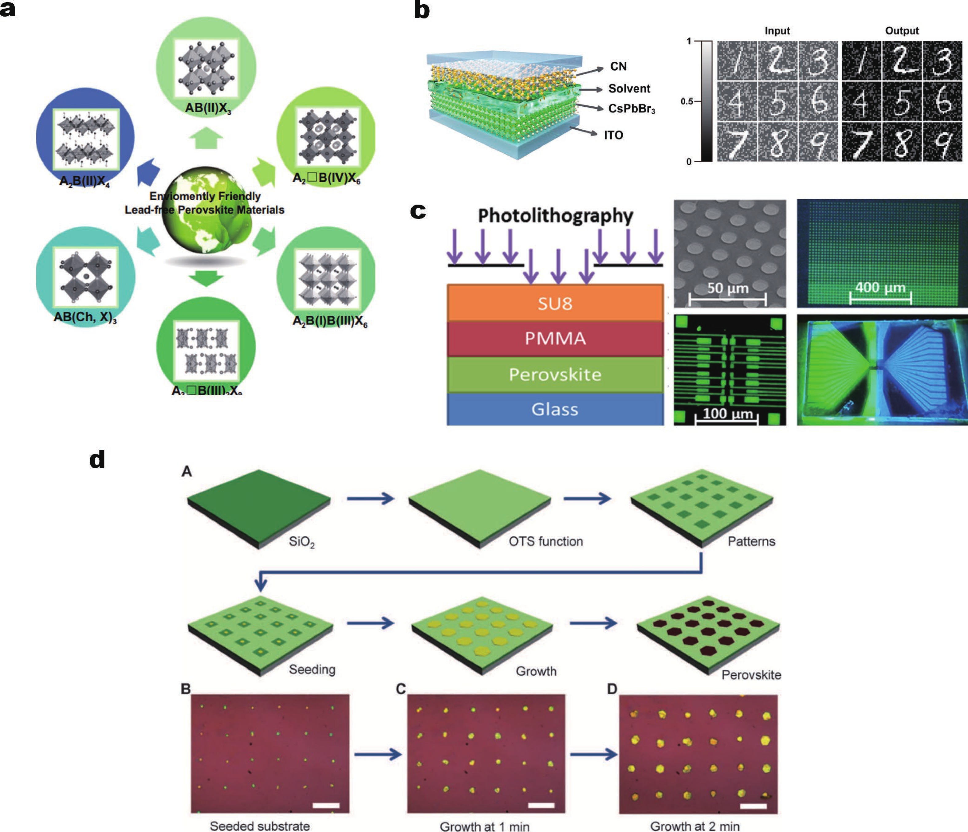
Fig. 4.  (Color online) Lead-free design and patterned integration of halide perovskites for practical optoelectronic synapses. (a) Representative lead-free perovskite compositions and material mechanisms for artificial synapses, highlighting how vacancy formation, band-structure modulation, and ion-migration-related conductance changes can regulate synaptic plasticity[76]. Adapted from Liu et al., Matter, 2024. (b) Representative lead-free Cs3Bi2I9 nanocrystal-based flexible optoelectronic synapse, showing light-induced synaptic behavior and neuromorphic visual recognition[77]. Adapted from Li et al., Research, 2024. (c) Top-down lithographic patterning of multicolor hybrid perovskite films using a SU8/PMMA bilayer resist strategy, enabling microscale perovskite patterns and multicolor pixel arrays for optoelectronic integration[78]. Adapted from Harwell et al., ACS Nano, 2019. (d) Wafer-scale position-controlled growth of perovskite microplate arrays for addressable photodetector and transistor integration, demonstrating how spatially defined crystal growth can bridge perovskite materials synthesis and integrated device arrays[79]. Adapted from Wang et al., Science Advances, 2015.

[1]
Horowitz M. 1.1 computing’s energy problem (and what we can do about it). 2014 IEEE International Solid-State Circuits Conference Digest of Technical Papers (ISSCC), 2014: 10
[2]
Ding G L, Li H, Zhao J Y, et al. Nanomaterials for flexible neuromorphics. Chem Rev, 2024, 124(22): 12738 doi: 10.1021/acs.chemrev.4c00369
[3]
Ding G L, Zhao J Y, Zhou K, et al. Porous crystalline materials for memories and neuromorphic computing systems. Chem Soc Rev, 2023, 52(20): 7071 doi: 10.1039/D3CS00259D
[4]
Chang Y, Na S Y, Ro Y G, et al. Robust biodegradable synapse with sub-biological energy and extended memory for intelligent reflexive system. Nat Commun, 2025, 16: 10610 doi: 10.1038/s41467-025-66511-3
[5]
Zhang H, Ye J Y, Gao M B, et al. Single-molecule neuromorphic device with aJ-level power consumption per switching. Nat Commun, 2026, 17: 4655 doi: 10.1038/s41467-026-71127-2
[6]
Guo L Q, Sun H X, Min L L, et al. Two-terminal perovskite optoelectronic synapse for rapid trained neuromorphic computation with high accuracy. Adv Mater, 2024, 36(27): 2402253 doi: 10.1002/adma.202402253
[7]
Kim H, Choi M J, Suh J M, et al. Quasi-2D halide perovskites for resistive switching devices with ON/OFF ratios above 109. NPG Asia Mater, 2020, 12: 21 doi: 10.1038/s41427-020-0202-2
[8]
Zhang Y T, Poddar S, Huang H, et al. Three-dimensional perovskite nanowire array–based ultrafast resistive RAM with ultralong data retention. Sci Adv, 2021, 7(36): eabg3788 doi: 10.1126/sciadv.abg3788
[9]
XITONG HONG X L. Review on metal halide perovskite-based optoelectronic synapses. Photonics Res, 2023, 11(5): 787
[10]
Guan X W, Lei Z H, Yu X C, et al. Low-dimensional metal-halide perovskites as high-performance materials for memory applications. Small, 2022, 18(38): 2203311 doi: 10.1002/smll.202203311
[11]
Rafique H, Abbas G, Mendes M J, et al. Recent advancements and perspectives of low-dimensional halide perovskites for visual perception and optoelectronic applications. Nano Micro Lett, 2025, 18(1): 44
[12]
Kim S I, Lee Y, Park M H, et al. Dimensionality dependent plasticity in halide perovskite artificial synapses for neuromorphic computing. Adv Electron Mater, 2019, 5(9): 1900008 doi: 10.1002/aelm.201900008
[13]
Im J H, Luo J S, Franckevičius M, et al. Nanowire perovskite solar cell. Nano Lett, 2015, 15(3): 2120 doi: 10.1021/acs.nanolett.5b00046
[14]
Spina M, Bonvin E, Sienkiewicz A, et al. Controlled growth of CH3NH3PbI3 nanowires in arrays of open nanofluidic channels. Sci Rep, 2016, 6: 19834 doi: 10.1038/srep19834
[15]
Zhang J, Yang X K, Deng H, et al. Low-dimensional halide perovskites and their advanced optoelectronic applications. Nano Micro Lett, 2017, 9(3): 36 doi: 10.1007/s40820-017-0137-5
[16]
Zhu Z H, Zhu C, Yang L, et al. Room-temperature epitaxial welding of 3D and 2D perovskites. Nat Mater, 2022, 21(9): 1042 doi: 10.1038/s41563-022-01311-4
[17]
Liu J Q, Gong J D, Wei H H, et al. A bioinspired flexible neuromuscular system based thermal-annealing-free perovskite with passivation. Nat Commun, 2022, 13: 7427 doi: 10.1038/s41467-022-35092-w
[18]
Zhou L E, Han S Y, Liu H, et al. Energy-efficient, stable, and temperature-tolerant neuromorphic device based on single crystals of halide perovskites. Cell Rep Phys Sci, 2024, 5(7): 102078 doi: 10.1016/j.xcrp.2024.102078
[19]
Babayigit A, Ethirajan A, Muller M, et al. Toxicity of organometal halide perovskite solar cells. Nat Mater, 2016, 15(3): 247 doi: 10.1038/nmat4572
[20]
Zhou Y Y, Zhao Y X. Chemical stability and instability of inorganic halide perovskites. Energy Environ Sci, 2019, 12(5): 1495 doi: 10.1039/C8EE03559H
[21]
Wang Y, Lv Z Y, Chen J R, et al. Photonic synapses based on inorganic perovskite quantum dots for neuromorphic computing. Adv Mater, 2018, 30(38): 1802883 doi: 10.1002/adma.201802883
[22]
Vishwanath S K, Karkera C, et al. Lead-free Cs3Bi2I9Perovskite memristors for energy-efficient neuromorphic computing. ACS Energy Lett, 2025, 10(5): 2193 doi: 10.1021/acsenergylett.5c00411
[23]
Du Y J, Yang J J, Lv Z Y, et al. Integration of perovskite/low-dimensional material heterostructures for optoelectronics and artificial visual systems. Adv Funct Mater, 2025, 35(36): 2500953 doi: 10.1002/adfm.202500953
[24]
Lin Y, Bai Y, Fang Y J, et al. Suppressed ion migration in low-dimensional perovskites. ACS Energy Lett, 2017, 2(7): 1571 doi: 10.1021/acsenergylett.7b00442
[25]
Meng Y, Zhong H K, Xu Z H, et al. Functionalizing nanophotonic structures with 2D van der Waals materials. Nanoscale Horiz, 2023, 8(10): 1345 doi: 10.1039/D3NH00246B
[26]
Yang P, Yu X P, Yu R J, et al. High polarization-sensitive synaptic transistor based on perovskite nanowire array for efficient biometric recognition. Adv Funct Mater, 2025, 35(11): 2416954 doi: 10.1002/adfm.202416954
[27]
Ghimire S, Klinke C. Two-dimensional halide perovskites: Synthesis, optoelectronic properties, stability, and applications. Nanoscale, 2021, 13(29): 12394 doi: 10.1039/D1NR02769G
[28]
Xia Y N, Yang P D, Sun Y G, et al. One-dimensional nanostructures: Synthesis, characterization, and applications. ChemInform, 2003, 34(22): 200322236 doi: 10.1002/chin.200322236
[29]
Pradhan B, Das S, Li J X, et al. Ultrasensitive and ultrathin phototransistors and photonic synapses using perovskite quantum dots grown from graphene lattice. Sci Adv, 2020, 6(7): eaay5225 doi: 10.1126/sciadv.aay5225
[30]
Long Z H, Qiu X, Chan C L J, et al. A neuromorphic bionic eye with filter-free color vision using hemispherical perovskite nanowire array retina. Nat Commun, 2023, 14: 1972 doi: 10.1038/s41467-023-37581-y
[31]
Liu Q, Wei Q, Ren H, et al. Circular polarization-resolved ultraviolet photonic artificial synapse based on chiral perovskite. Nat Commun, 2023, 14: 7179 doi: 10.1038/s41467-023-43034-3
[32]
Bao C X, Yang J, Bai S, et al. High performance and stable all-inorganic metal halide perovskite-based photodetectors for optical communication applications. Adv Mater, 2018, 30(38): 1803422 doi: 10.1002/adma.201803422
[33]
Wang H P, Li S Y, Liu X Y, et al. Low-dimensional metal halide perovskite photodetectors. Adv Mater, 2021, 33(7): 2003309 doi: 10.1002/adma.202003309
[34]
Feng J G, Gong C, Gao H F, et al. Single-crystalline layered metal-halide perovskite nanowires for ultrasensitive photodetectors. Nat Electron, 2018, 1(7): 404 doi: 10.1038/s41928-018-0101-5
[35]
Zhu H M, Fu Y P, Meng F, et al. Lead halide perovskite nanowire lasers with low lasing thresholds and high quality factors. Nat Mater, 2015, 14(6): 636 doi: 10.1038/nmat4271
[36]
Vasilopoulou M, bin Mohd Yusoff A R, Chai Y, et al. Neuromorphic computing based on halide perovskites. Nat Electron, 2023, 6(12): 949 doi: 10.1038/s41928-023-01082-z
[37]
John R A, Demirağ Y, Shynkarenko Y, et al. Reconfigurable halide perovskite nanocrystal memristors for neuromorphic computing. Nat Commun, 2022, 13: 2074 doi: 10.1038/s41467-022-29727-1
[38]
Kim S J, Im I H, Baek J H, et al. Linearly programmable two-dimensional halide perovskite memristor arrays for neuromorphic computing. Nat Nanotechnol, 2025, 20(1): 83 doi: 10.1038/s41565-024-01790-3
[39]
Gao S, Liu G, Yang H L, et al. An oxide Schottky junction artificial optoelectronic synapse. ACS Nano, 2019, 13(2): 2634 doi: 10.1021/acsnano.9b00340
[40]
Liu K Q, Zhang T, Dang B J, et al. An optoelectronic synapse based on α-In2Se3 with controllable temporal dynamics for multimode and multiscale reservoir computing. Nat Electron, 2022, 5(11): 761 doi: 10.1038/s41928-022-00847-2
[41]
Xu H Y, Xu Z H, Ren Q Q, et al. Two-dimensional materials for integrated sensing. Nat Mater, 2026: 1
[42]
Yang Z Y, Huo S D, Zhang Z, et al. High-precision multibit opto-electronic synapses based on ReS2/h-BN/graphene heterostructure for energy-efficient and high-accuracy neuromorphic computing. Adv Funct Mater, 2025, 35(48): 2509119 doi: 10.1002/adfm.202509119
[43]
Zhou F C, Chai Y. Near-sensor and in-sensor computing. Nat Electron, 2020, 3(11): 664 doi: 10.1038/s41928-020-00501-9
[44]
Huang C Y, Li H C, Wu Y, et al. Inorganic halide perovskite quantum dots: A versatile nanomaterial platform for electronic applications. Nano Micro Lett, 2022, 15(1): 16
[45]
Cheng Y C, Li H, Liu B, et al. Vertical 0D-perovskite/2D-MoS2 van der Waals heterojunction phototransistor for emulating photoelectric-synergistically classical Pavlovian conditioning and neural coding dynamics. Small, 2020, 16(45): 2005217 doi: 10.1002/smll.202005217
[46]
Li J X, Dwivedi P, Kumar K S, et al. Growing perovskite quantum dots on carbon nanotubes for neuromorphic optoelectronic computing. Adv Electron Mater, 2021, 7(1): 2000535 doi: 10.1002/aelm.202000535
[47]
Meng Y, Feng J G, Han S, et al. Photonic van der Waals integration from 2D materials to 3D nanomembranes. Nat Rev Mater, 2023, 8(8): 498 doi: 10.1038/s41578-023-00558-w
[48]
Gu L L, Poddar S, Lin Y J, et al. A biomimetic eye with a hemispherical perovskite nanowire array retina. Nature, 2020, 581(7808): 278 doi: 10.1038/s41586-020-2285-x
[49]
Zhou Y, Sun Z B, Ding Y C, et al. An ultrawide field-of-view pinhole compound eye using hemispherical nanowire array for robot vision. Sci Robot, 2024, 9(90): eadi8666 doi: 10.1126/scirobotics.adi8666
[50]
Ren W, Zhao X M, Tang J, et al. A self-powered spherical compound eye with 8 ns-motion response for source-constrained drones. Nat Commun, 2026, 17: 6864 doi: 10.1038/s41467-026-73745-2
[51]
Liu Q, Wang P Z, Wei Q, et al. Chiral perovskite nanowire optoelectronic synapse for full-stokes polarization-resolved perception and reservoir computing. Adv Funct Mater, 2025, 35(8): 2415551 doi: 10.1002/adfm.202415551
[52]
Wang Y, Lei J C, Wang X, et al. Tear-film-inspired moisture-resistant and mechanical flexible perovskite microwire artificial visual system. Laser Photonics Rev, 2026, 20(13): e03181 doi: 10.1002/lpor.202503181
[53]
Ma F M, Zhu Y B, Xu Z W, et al. Optoelectronic perovskite synapses for neuromorphic computing. Adv Funct Mater, 2020, 30(11): 1908901 doi: 10.1002/adfm.201908901
[54]
Hong X T, Huang Y L, Tian Q L, et al. Two-dimensional perovskite-gated AlGaN/GaN high-electron-mobility-transistor for neuromorphic vision sensor. Adv Sci, 2022, 9(27): 2202019 doi: 10.1002/advs.202202019
[55]
Li Y T, Li J Z, Ren L, et al. Light-controlled reconfigurable optical synapse based on carbon nanotubes/2D perovskite heterostructure for image recognition. ACS Appl Mater Interfaces, 2022, 14(24): 28221 doi: 10.1021/acsami.2c05818
[56]
Gong J D, Wei H H, Liu J Q, et al. An artificial visual nerve for mimicking pupil reflex. Matter, 2022, 5(5): 1578 doi: 10.1016/j.matt.2022.02.020
[57]
Liu F, Zhang X Y, Valencia A, et al. Low energy consumption and stable perovskite-based photonic synapse with two-terminal lateral configuration. Nano Energy, 2025, 142: 111145 doi: 10.1016/j.nanoen.2025.111145
[58]
Sahu D, Nandi S J, et al. Ultralow energy optoelectronic synapse using halide perovskite/organic semiconductor heterostructure for neuromorphic computing, optical logic and wireless communication. ACS Appl Mater Interfaces, 2026, 18(18): 26509 doi: 10.1021/acsami.6c03922
[59]
Dan S, Paramanik S, Pal A J. Introducing chiro-optical activities in photonic synapses for neuromorphic computing and in-memory logic operations. ACS Nano, 2024, 18(22): 14457 doi: 10.1021/acsnano.4c01202
[60]
Zhou X, Hu F Z, Hou Q, et al. All-photonic artificial synapses based on photochromic perovskites for noncontact neuromorphic visual perception. Commun Mater, 2024, 5: 116 doi: 10.1038/s43246-024-00553-w
[61]
Liu Y, Wang B, Wu L, et al. Artificial visual synaptic architecture with high-linearity light-modulated weight for optoelectronic neuromorphic computing. ACS Appl Mater Interfaces, 2023, 15(44): 51380 doi: 10.1021/acsami.3c11495
[62]
Xia J N, Gao C S, Peng C Y, et al. Multidimensional deep ultraviolet (DUV) synapses based on organic/perovskite semiconductor heterojunction transistors for antispoofing facial recognition systems. Nano Lett, 2024, 24(22): 6673 doi: 10.1021/acs.nanolett.4c01356
[63]
Xie C, University A, Li C, et al. Electron trapping enhanced deep-ultraviolet optoelectronic synapses based on two-dimensional wide-bandgap perovskite/organic-semiconductor heterojunctions. Nano Lett, 2025, 25(40): 14686 doi: 10.1021/acs.nanolett.5c03851
[64]
Cui D S, University X, et al. Self-powered halide perovskite optoelectronic synaptic memristors for reconfigurable logic and reservoir computing applications. Nano Lett, 2025, 25(43): 15705 doi: 10.1021/acs.nanolett.5c04297
[65]
Huang W, Tang J W, Li B, et al. Design of all-optical bidirectional self-powered synaptic devices for neuromorphic computing applications. Small, 2025, 21(34): 2505327 doi: 10.1002/smll.202505327
[66]
Yang X Y, Xiong Z Y, Chen Y J, et al. A self-powered artificial retina perception system for image preprocessing based on photovoltaic devices and memristive arrays. Nano Energy, 2020, 78: 105246 doi: 10.1016/j.nanoen.2020.105246
[67]
Lin Q H, Zhu Y B, Hu X, et al. Multifunctional PN optoelectronic synapse and its smart integration towards augmented artificial visual system. npj Flex Electron, 2025, 9: 81 doi: 10.1038/s41528-025-00459-8
[68]
Shao H, Li Y Q, Yang W, et al. A reconfigurable optoelectronic synaptic transistor with stable Zr-CsPbI3 nanocrystals for visuomorphic computing. Adv Mater, 2023, 35(12): 2208497 doi: 10.1002/adma.202208497
[69]
Poddar S, Khan B, Kumar S, et al. Ultra-high density perovskite nanowire array memristor-based multi-layer perceptron. Nat Commun, 2026, 17: 5576 doi: 10.1038/s41467-026-71372-5
[70]
Miao J S, Song B, Xu Z H, et al. Single pixel black phosphorus photodetector for near-infrared imaging. Small, 2018, 14(2): 1702082 doi: 10.1002/smll.201702082
[71]
Zhou Y, Fu J W, Chen Z R, et al. Computational event-driven vision sensors for in-sensor spiking neural networks. Nat Electron, 2023, 6(11): 870 doi: 10.1038/s41928-023-01055-2
[72]
Chien Y C, Xiang H, Shi Y F, et al. A MoS2 hafnium oxide based ferroelectric encoder for temporal-efficient spiking neural network. Adv Mater, 2023, 35(2): 2204949 doi: 10.1002/adma.202204949
[73]
Liu S X, Wu Z X, He Z L, et al. Low-power perovskite neuromorphic synapse with enhanced photon efficiency for directional motion perception. ACS Appl Mater Interfaces, 2024, 16(17): 22303 doi: 10.1021/acsami.4c04398
[74]
Zi J Z, Sun J, Yang B, et al. Multidimensional and reconfigurable optical neuromorphic computing using perovskite-based all-photonic synapses. Commun Mater, 2026, 7: 92 doi: 10.1038/s43246-026-01097-x
[75]
Wang H, Lin R Y, Zhao K B, et al. Dual-way alternation sensing memristors based on (BA)2(MA)3Pb4Br13 ferroelectric quantum dots with sub-0.16 V switching for broadband image-recognition systems. Adv Funct Mater, 2025, 35(46): 2510543 doi: 10.1002/adfm.202510543
[76]
Liu S J, Cheng Z P, Li M Y, et al. Synapses based on lead-free perovskite in artificial intelligence. Matter, 2024, 7(9): 2810
[77]
Li M C, Li C, Ye K, et al. Self-powered photonic synapses with rapid optical erasing ability for neuromorphic visual perception. Research, 2024, 7: 526
[78]
Harwell J, Burch J, Fikouras A, et al. Patterning multicolor hybrid perovskite FilmsviaTop-down lithography. ACS Nano, 2019, 13(4): 3823
[79]
Wang G M, Li D H, Cheng H C, et al. Wafer-scale growth of large arrays of perovskite microplate crystals for functional electronics and optoelectronics. Sci Adv, 2015, 1(9): e1500613
[80]
Wang R, Wang J T, Tan S, et al. Opportunities and challenges of lead-free perovskite optoelectronic devices. Trends Chem, 2019, 1(4): 368
[81]
Wang M, Wang W, Ma B, et al. Lead-Free Perovskite Materials for Solar Cells. Nano-Micro Letters, 2021, 13(1), 62 [81] Wang M H, Wang W, Ma B, et al. Lead-free perovskite materials for solar cells. Nano Micro Lett, 2021, 13(1): 62
[82]
Zhang Y Q, Ma Y, Wang Y X, et al. Lead-free perovskite photodetectors: Progress, challenges, and opportunities. Adv Mater, 2021, 33(26): 2006691
[83]
Kwak K J, Baek J H, Lee D E, et al. Ambient stable all inorganic CsCu2I3 artificial synapses for neurocomputing. Nano Lett, 2022, 22(14): 6010
[84]
Zheng Y Q, Xu H Y, Xu H, et al. Twelve-inch electrically anisotropic boridene for optoelectronic computing. Nat Nanotechnol, 2026, 21(4): 571
[85]
Zhang Z, Tian Q J, Huo S D, et al. Photodoping strategies in two-dimensional semiconductors: Mechanisms, characterizations, and emerging applications. InfoMat, 2025, 7(12): e70092
[86]
Jeong B, Han H, Park C. Micro- and nanopatterning of halide perovskites where crystal engineering for emerging photoelectronics meets integrated device array technology. Adv Mater, 2020, 32(30): 2000597
[87]
Wang K Y, Xing G C, Song Q H, et al. Micro- and nanostructured lead halide perovskites: From materials to integrations and devices. Adv Mater, 2021, 33(6): 2000306
[88]
Xu Z H, Chin S H, Park B I, et al. Advancing perovskite solar cell commercialization: Bridging materials, vacuum deposition, and AI-assisted automation. Next Mater, 2024, 3: 100103
[89]
Liang L M, Ma T, Chen Z Y, et al. Patterning technologies for metal halide perovskites: A review. Adv Mater Technol, 2023, 8(3): 2200419
[90]
Lyashenko D, Perez A, Zakhidov A. High-resolution patterning of organohalide lead perovskite pixels for photodetectors using orthogonal photolithography. Phys Status Solidi A, 2017, 214(1): 1600302
[91]
Cegielski P J, Giesecke A L, Neutzner S, et al. Monolithically integrated perovskite SemiconductorLasers on silicon photonic chips by scalable top-down fabrication. Nano Lett, 2018, 18(11): 6915
[92]
Gu Z K, Wang K, Li H Z, et al. Direct-writing multifunctional perovskite single crystal arrays by inkjet printing. Small, 2017, 13(8): 1603217
[93]
Chou S S, Swartzentruber B S, Foley-Janish M T, et al. Laser direct write synthesis of lead halide perovskites. J Phys Chem Lett, 2016, 7(19): 3736
[94]
Zhizhchenko A, Syubaev S, Berestennikov A, et al. Single-mode lasing from imprinted halide-perovskite microdisks. ACS Nano, 2019, 13(4): 4140
[95]
Niu L, Liu X F, Cong C X, et al. Controlled synthesis of organic/inorganic van der Waals solid for tunable light–matter interactions. Adv Mater, 2015, 27(47): 7800
[96]
Wu E X, Wang Y, Huo S D, et al. Universal core–shell nanowire memristor platform with quasi-2D filament confinement for scalable neuromorphic applications. Adv Funct Mater, 2026, 36(11): e18764
[97]
Liu Y, Huang Y, Duan X F. Van der Waals integration before and beyond two-dimensional materials. Nature, 2019, 567(7748): 323
[98]
Kum H S, Lee H, Kim S, et al. Heterogeneous integration of single-crystalline complex-oxide membranes. Nature, 2020, 578(7793): 75
[99]
Meng Y, Mao W, Xu Z, et al. Heterogeneous photonic integration of single-crystalline nanomembranes. Research Square Preprint, 2025, DOI: 10.1038/s41586-026-11000-w
[100]
Kaur P, Boes A, Ren G H, et al. Hybrid and heterogeneous photonic integration. APL Photonics, 2021, 6(6): 061102
[101]
Pintus P, Dumont M, Shah V, et al. Integrated non-reciprocal magneto-optics with ultra-high endurance for photonic in-memory computing. Nat Photonics, 2025, 19(1): 54
[102]
Geler-Kremer J, Eltes F, Stark P, et al. A ferroelectric multilevel non-volatile photonic phase shifter. Nat Photonics, 2022, 16(7): 491
[103]
Xu H Y, Xie R Z, Miao J S, et al. Critical band-to-band-tunnelling based optoelectronic memory. Light Sci Appl, 2025, 14: 72
[104]
Kang J H, Shin H, Kim K S, et al. Monolithic 3D integration of 2D materials-based electronics towards ultimate edge computing solutions. Nat Mater, 2023, 22(12): 1470
  • Search

    Advanced Search >>

    GET CITATION

    shu

    Export: BibTex EndNote

    Article Metrics

    Article views: 3 Times PDF downloads: 1 Times Cited by: 0 Times

    History

    Received: 17 June 2026 Revised: 14 August 2026 Online: Accepted Manuscript: 23 September 2026

    Catalog

      Email This Article

      User name:
      Email:*请输入正确邮箱
      Code:*验证码错误
      Zhihao Xu, Yingjie Luo, Alson Yau, Yuan Meng, Seung-il Kim, Kyubeen Kim, Sheng Ran, Sang-Hoon Bae. Low-dimensional perovskite optoelectronic synapses for neuromorphic vision[J]. Journal of Semiconductors, 2026, In Press. doi: 10.1088/1674-4926/26060035 ****Z H Xu, Y J Luo, A Yau, Y Meng, S Kim, K Kim, S Ran, and S Bae, Low-dimensional perovskite optoelectronic synapses for neuromorphic vision[J]. J. Semicond., 2026, accepted doi: 10.1088/1674-4926/26060035
      Citation:
      Zhihao Xu, Yingjie Luo, Alson Yau, Yuan Meng, Seung-il Kim, Kyubeen Kim, Sheng Ran, Sang-Hoon Bae. Low-dimensional perovskite optoelectronic synapses for neuromorphic vision[J]. Journal of Semiconductors, 2026, In Press. doi: 10.1088/1674-4926/26060035 ****
      Z H Xu, Y J Luo, A Yau, Y Meng, S Kim, K Kim, S Ran, and S Bae, Low-dimensional perovskite optoelectronic synapses for neuromorphic vision[J]. J. Semicond., 2026, accepted doi: 10.1088/1674-4926/26060035

      Low-dimensional perovskite optoelectronic synapses for neuromorphic vision

      DOI: 10.1088/1674-4926/26060035
      CSTR: 32376.14.1674-4926.26060035
      More Information
      • Zhihao Xu received his bachelor's degree from the School of Precision Instruments and Optoelectronics Engineering at Tianjin University in 2017 and his master's degree from the same institution in 2020. He is currently pursuing his Ph.D. degree at Washington University in St. Louis
      • Yingjie Luo received his bachelor's degree from South China University of Technology in 2021 and his master's degree from the same institution in 2024. He is currently pursuing his Ph.D. degree in Physics at Washington University in St. Louis
      • Alson Yau is currently an undergraduate student at Washington University in St. Louis under the supervision of Prof. Sang-Hoon Bae
      • Sang-Hoon Bae received his bachelor's and master's degrees from Sungkyunkwan University in 2011 and 2013, respectively, and his Ph.D. degree in materials science and engineering from the University of California, Los Angeles, in 2017. He is currently an Assistant Professor at Washington University in St. Louis. His research focuses on advanced materials, heterogeneous integration, and AI hardware
      • Corresponding author: sbae22@wustl.edu
      • Received Date: 2026-06-17
      • Revised Date: 2026-08-14
      • Available Online: 2026-09-23

      Catalog

        /

        DownLoad:  Full-Size Img  PowerPoint
        Return
        Return