J. Semicond. >  Just Accepted

ARTICLES

Sparse wafer metrology for semiconductor process control with physics-informed diagnostics

Hua Zhang1, Yingtao Guo1, Longhua Liu1, Zhigang Song1, 2, 3, and Wanhua Zheng1, 2, 3,

+ Author Affiliations

 Corresponding author: Zhigang Song, songzhigang@semi.ac.cn; Wanhua Zheng, whzheng@semi.ac.cn

DOI: 10.1088/1674-4926/26070009CSTR: 32376.14.1674-4926.26070009

PDF

Turn off MathJax

Abstract: Production-compatible wafer-thickness metrology often samples fewer than ten sites per wafer, limiting process-control decisions. This work evaluates what such sparse measurements can support, when physics priors add value, and where additional measurements are needed. We combine MOCVD and MBE simulators, leakage-safe Polynomial Ridge and XGBoost predictors, and a physics-informed Kolmogorov-Arnold Network (PI-KAN) with a weak transport-diffusion residual. Eleven reconstruction methods are tested on public wafer data comprising MOVPE/AlN, hBN, and OpenMV silicon wafers. For OpenMV mean-thickness screening, Polynomial Ridge and XGBoost reach test $R^2 \geq 0.996$ with $C_{pk} \geq 2.63$; these high values largely reflect the known eight-site mean baseline, and the incremental ML improvement is 0.050–0.053 nm. On the MOVPE benchmark, Quadratic Ridge and Gaussian Process tie for the best protocol-summary score, while PI-KAN ranks lower but supplies diagnostic value: its PDE residual correlates with reconstruction error ($\rho = 0.698$, $p = 0.008$), and model-disagreement signals correlate with held-out error. The results support an offline tiered metrology strategy: classical baselines for screening, physics-regularized overlays for diagnosis, and triggered measurements for local edge or anomaly decisions.

Keywords: sparse wafer metrologysemiconductor process controlepitaxial thicknessMOCVDMBEphysics-informed machine learning


[1]
Hite J K. A review of homoepitaxy of III-nitride semiconductors by metal organic chemical vapor deposition and the effects on vertical devices. Crystals, 2023, 13(3): 387 doi: 10.3390/cryst13030387
[2]
Li X H, Xu Q, Zhang Z Y. Molecular beam epitaxy growth of quantum wires and quantum dots. Nanomaterials, 2023, 13(6): 960 [PubMed]
[3]
Wang B, Zeng Y G, Song Y, et al. Principles of selective area epitaxy and applications in III–V semiconductor lasers using MOCVD: A review. Crystals, 2022, 12(7): 1011. doi: 10.3390/cryst12071011
[4]
Lan X, Cheng Y L, Yang X D, et al. Wafer-scale engineering of two-dimensional transition metal dichalcogenides. Chip, 2023, 2(3): 100057 doi: 10.1016/j.chip.2023.100057
[5]
Liu Z J, Gong X G, Cheng J R, et al. Wafer-scale synthesis of two-dimensional materials for integrated electronics. Chip, 2024, 3(1): 100080 doi: 10.1016/j.chip.2023.100080
[6]
Gallagher J C, Mastro M A, Ebrish M A, et al. Using machine learning with optical profilometry for GaN wafer screening. Sci Rep, 2023, 13: 3352 doi: 10.1038/s41598-023-29107-9
[7]
Miller W, Schulz T, Lymperakis L, et al. Kinetic Monte Carlo simulations for AlN and AlGaN epitaxial growth on AlN. J Cryst Growth, 2023, 607: 127125 doi: 10.1016/j.jcrysgro.2023.127125
[8]
Li Y, Chen X, Ai W. Kinetic Monte Carlo simulation study of the early stages of epitaxial SiC (0001) growth. J Cryst Growth, 2023, 617: 127291 doi: 10.1016/j.jcrysgro.2023.127291
[9]
Momeni K, Ji Y, Nayir N, et al. A computational framework for guiding the MOCVD-growth of wafer-scale 2D materials. npj Comput Mater, 2022, 8: 240 doi: 10.1038/s41524-022-00936-y
[10]
He Y, Wang J, Luo T, et al. Analysis and optimization of MOCVD flow ratio based on machine learning and PSO algorithm. J Cryst Growth, 2022, 590: 126683 doi: 10.1016/j.jcrysgro.2022.126683
[11]
Lee J, Jin J. A novel method to design and evaluate artificial neural network for thin film thickness measurement traceable to the length standard. Sci Rep, 2022, 12: 2212 doi: 10.1038/s41598-022-06247-y
[12]
Shen C, Zhan W, Pan S, et al. Real-time self-optimization of quantum dot laser emissions during machine learning-assisted epitaxy. Adv Sci, 2025, 12(27): 2503059 doi: 10.1002/advs.202503059
[13]
Kapoor S, Narayanan A. Leakage and the reproducibility crisis in machine-learning-based science. Patterns, 2023, 4(9): 100804 doi: 10.1016/j.patter.2023.100804
[14]
Merchant A, Batzner S, Schoenholz S S, et al. Scaling deep learning for materials discovery. Nature, 2023, 624(7990): 80 doi: 10.1038/s41586-023-06735-9
[15]
Hirtz J, Li H, Zhao X, et al. TCAD augmented machine learning for semiconductor device failure troubleshooting and reverse engineering. J Semicond, 2021, 42(12): 124102
[16]
Cheng B, Wang Y, Wang C, et al. Computer vision based in-situ TEM image analysis by using features of shallow neural network. J Semicond, 2022, 43(8): 081001 doi: 10.1088/1674-4926/43/8/081001
[17]
Lei M, Pan S, Hao D, et al. Defect control of photoresist etch-back process based on plasma parameters. J Semicond, 2026, 47(3): 032401 doi: 10.1088/1674-4926/25090008
[18]
Liu D Y, Xu L M, Lin X M, et al. Machine learning for semiconductors. Chip, 2022, 1(4): 100033 doi: 10.1016/j.chip.2022.100033
[19]
Zhao X Z, Li A, Zhang J M, et al. Programmable photonics-empowered ultralow-cost photonic device metrology. Chip, 2026: 100200
[20]
Pampili P, Pristovsek M. Nitrogen-polar growth of AlN on vicinal (0001) sapphire by MOVPE. J Appl Phys, 2024, 135(19): 195303 doi: 10.1063/5.0202746
[21]
Sobolá I M. Global sensitivity indices for nonlinear mathematical models and their Monte Carlo estimates. Math Comput Simul, 2001, 55(1/2/3): 271
[22]
Herman J, Usher W. SALib: An open-source Python library for sensitivity analysis. J Open Source Softw, 2017, 2(9): 97 doi: 10.21105/joss.00097
[23]
To T B T, Almeida R, Ferreira S O, et al. Roughness and correlations in the transition from island to film growth: Simulations and application to CdTe deposition. Appl Surf Sci, 2021, 560: 149946 doi: 10.1016/j.apsusc.2021.149946
[24]
Peyré G, Cuturi M. Computational optimal transport with applications to data sciences. Found Trends® Mach Learn, 2019, 11(5/6): 355
[25]
Irandoukht A. Optimum ridge regression parameter using R-squared of prediction as a criterion for regression analysis. J Stat Theory Appl, 2021, 20(2): 242
[26]
Chen T Q, Guestrin C. XGBoost: A scalable tree boosting system. Proceedings of the 22nd ACM SIGKDD International Conference on Knowledge Discovery and Data Mining. San Francisco California USA. ACM, 2016: 785
[27]
Sagi O, Rokach L. Approximating XGBoost with an interpretable decision tree. Inf Sci, 2021, 572: 522 doi: 10.1016/j.ins.2021.05.055
[28]
Bentéjac C, Csörgő A, Martínez-Muñoz G. A comparative analysis of gradient boosting algorithms. Artif Intell Rev, 2021, 54(3): 1937 doi: 10.1007/s10462-020-09896-5
[29]
Ke G, Meng Q, Finley T, et al. LightGBM: A highly efficient gradient boosting decision tree. Advances in Neural Information Processing Systems, 2017: 3146
[30]
Kane V E. Process capability indices. J Qual Technol, 1986, 18(1): 41 doi: 10.1080/00224065.1986.11978984
[31]
Liu Z, Wang Y, Vaidya S, et al. KAN: Kolmogorov-Arnold networks. The Thirteenth International Conference on Learning Representations, 2025(补充卷期页码)
[32]
Zhang X Y, Zhou H J. Generalization bounds and model complexity for Kolmogorov-Arnold networks. 2024: arXiv: 2410.08026. https://arxiv.org/abs/2410.08026
[33]
Raissi M, Perdikaris P, Karniadakis G E. Physics-informed neural networks: A deep learning framework for solving forward and inverse problems involving nonlinear partial differential equations. J Comput Phys, 2019, 378: 686 doi: 10.1016/j.jcp.2018.10.045
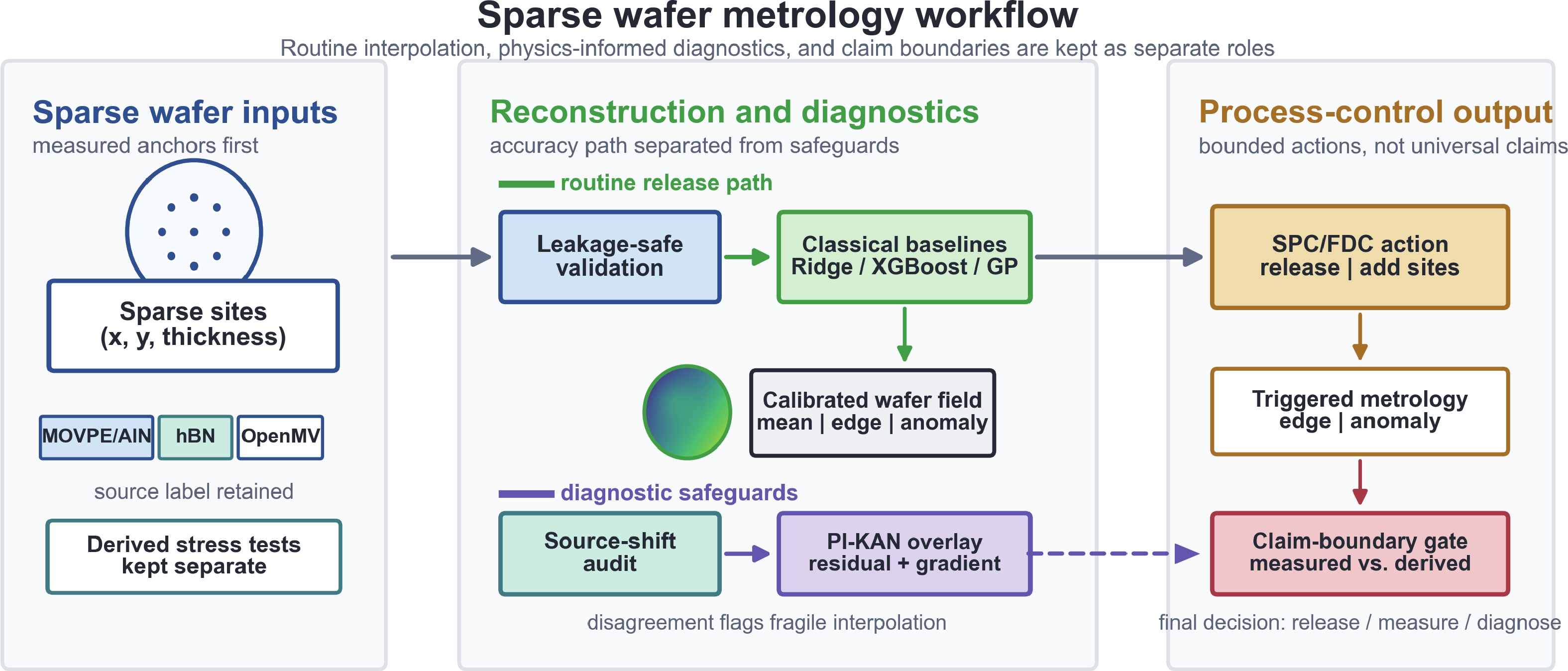
Fig. 1.  (Color online) Sparse wafer metrology workflow for semiconductor process control. Sparse measured sites and source labels enter a routine release path in which leakage-safe validation and classical baselines reconstruct a calibrated wafer field for SPC/FDC screening. A separate diagnostic path uses source-shift auditing and the PI-KAN residual/gradient overlay to flag fragile interpolation and trigger additional metrology. The claim-boundary gate separates measured evidence from derived stress tests and avoids treating diagnostic disagreement as universal PI-KAN accuracy dominance.

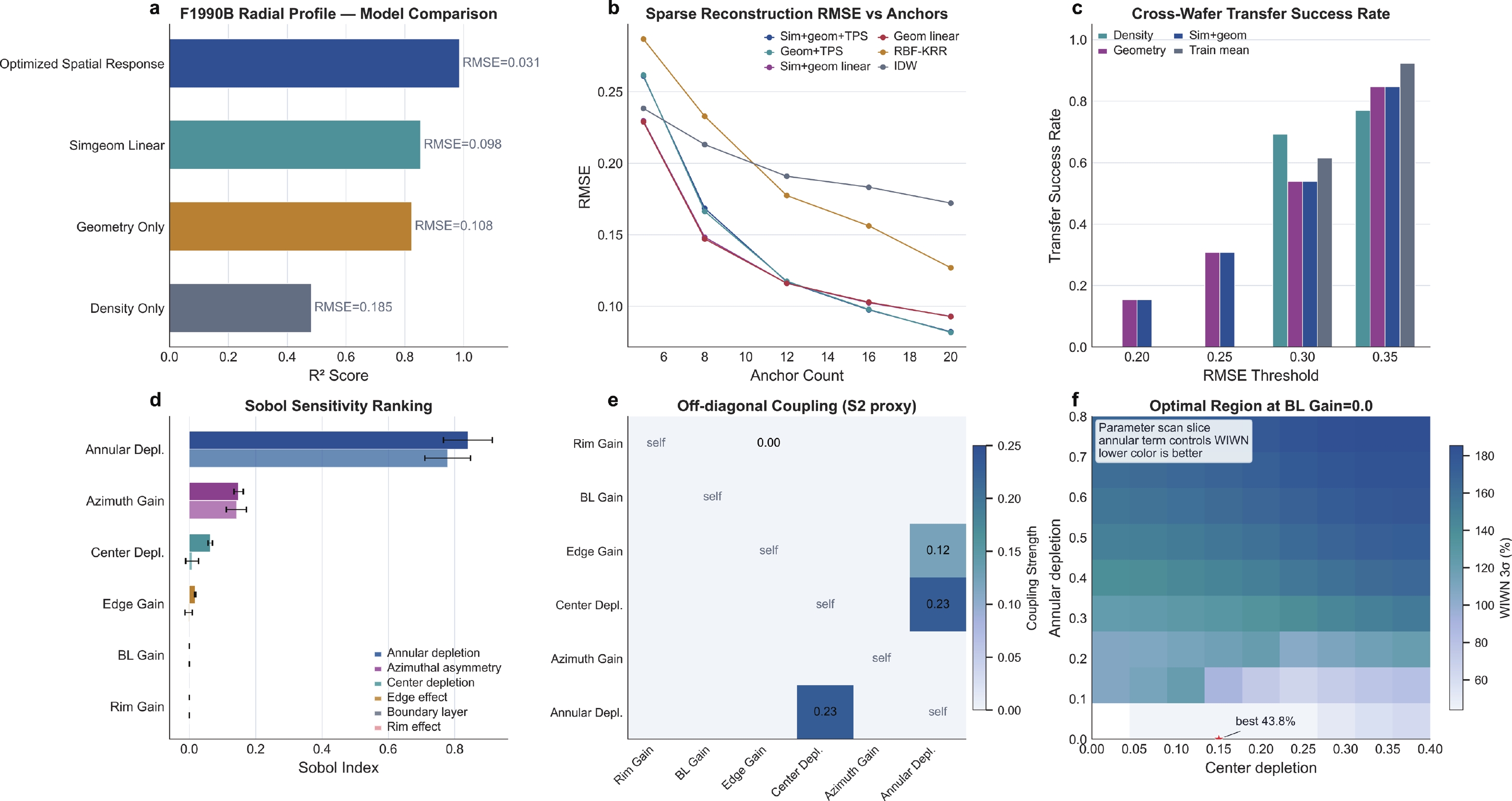
Fig. 2.  (Color online) MOCVD real-data morphology comparison using the Zenodo MOVPE/AlN F1990B thickness map. Panels compare measured thickness, optimized continuous flux field, radial profiles, cross-validated predictions, residuals, and model controls.

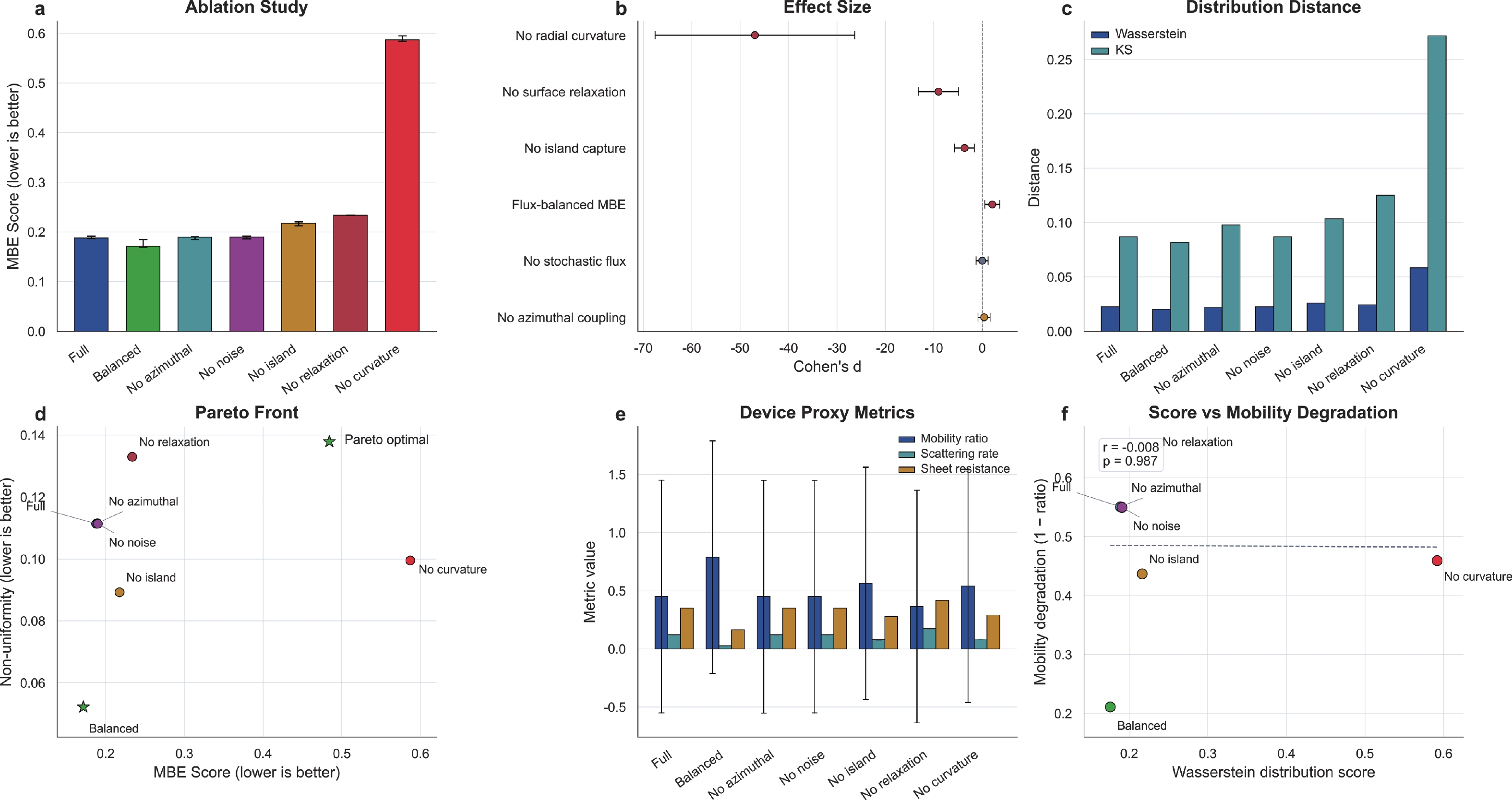
Fig. 3.  (Color online) MBE simulation and real-wafer distribution comparison. Panels report roughness evolution, final surface morphology, real-versus-virtual nine-site non-uniformity distributions, site-wise signatures, and parameter-scan behavior.

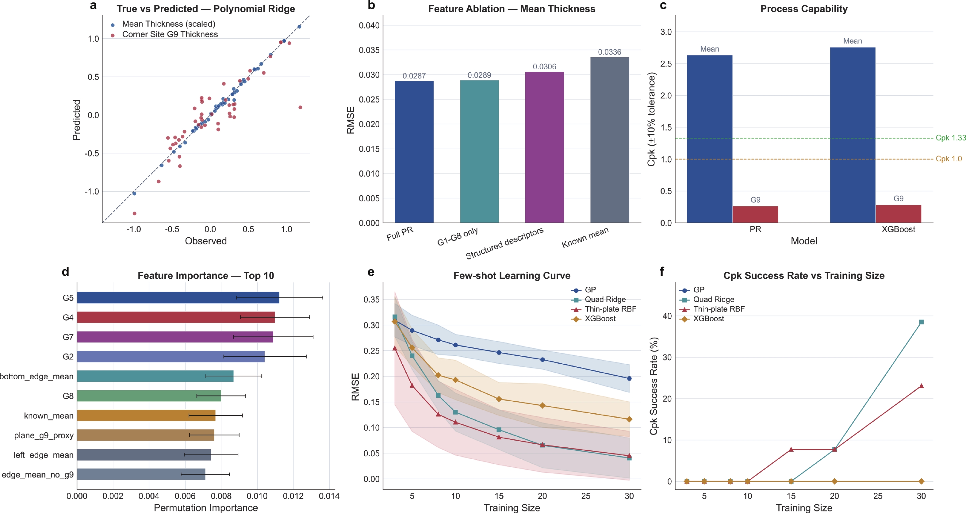
Fig. 4.  (Color online) Polynomial Ridge real-wafer benchmark on the OpenMV silicon wafer dataset ($ n = 184 $). (a) True vs. predicted thickness for mean-thickness and G9 corner-site targets. (b) Feature ablation comparing full PR, G1–G8 only, structured descriptors, and known-mean baselines. (c) Process capability index $ C_{pk} $ at ±10% tolerance. (d) Top-10 permutation feature importance. (e) Few-shot learning curve across training sizes $ n \in [3, 30] $. (f) $ C_{pk} $ success rate vs. training size

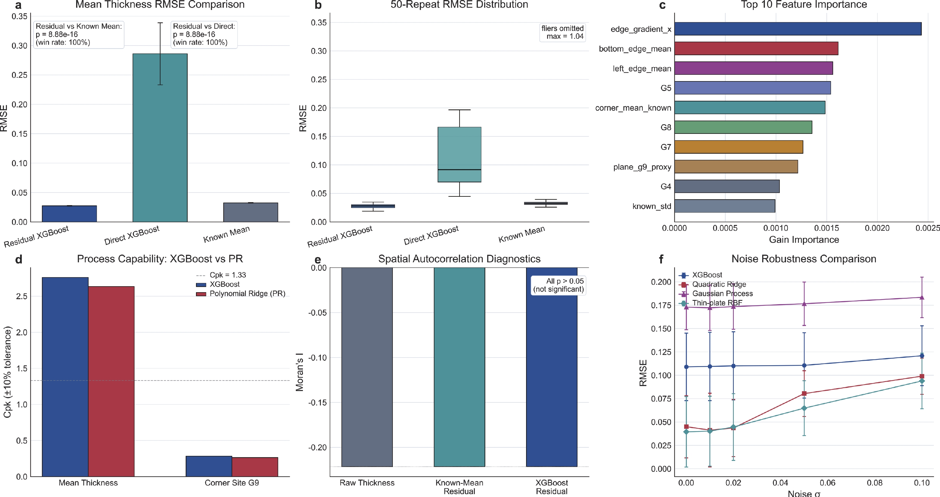
Fig. 5.  (Color online) XGBoost residual-correction benchmark on real wafer data. (a) Mean-thickness RMSE comparison among residual XGBoost, direct XGBoost, and known-mean baseline with paired Wilcoxon $ p $-values. (b) 50-repeat RMSE distribution. (c) Top-10 gain feature importance. (d) Process capability $ C_{pk} $ comparison between XGBoost and PR. (e) Spatial autocorrelation diagnostics (Moran's $ I $, Geary's $ C $). (f) Noise robustness comparison across methods.

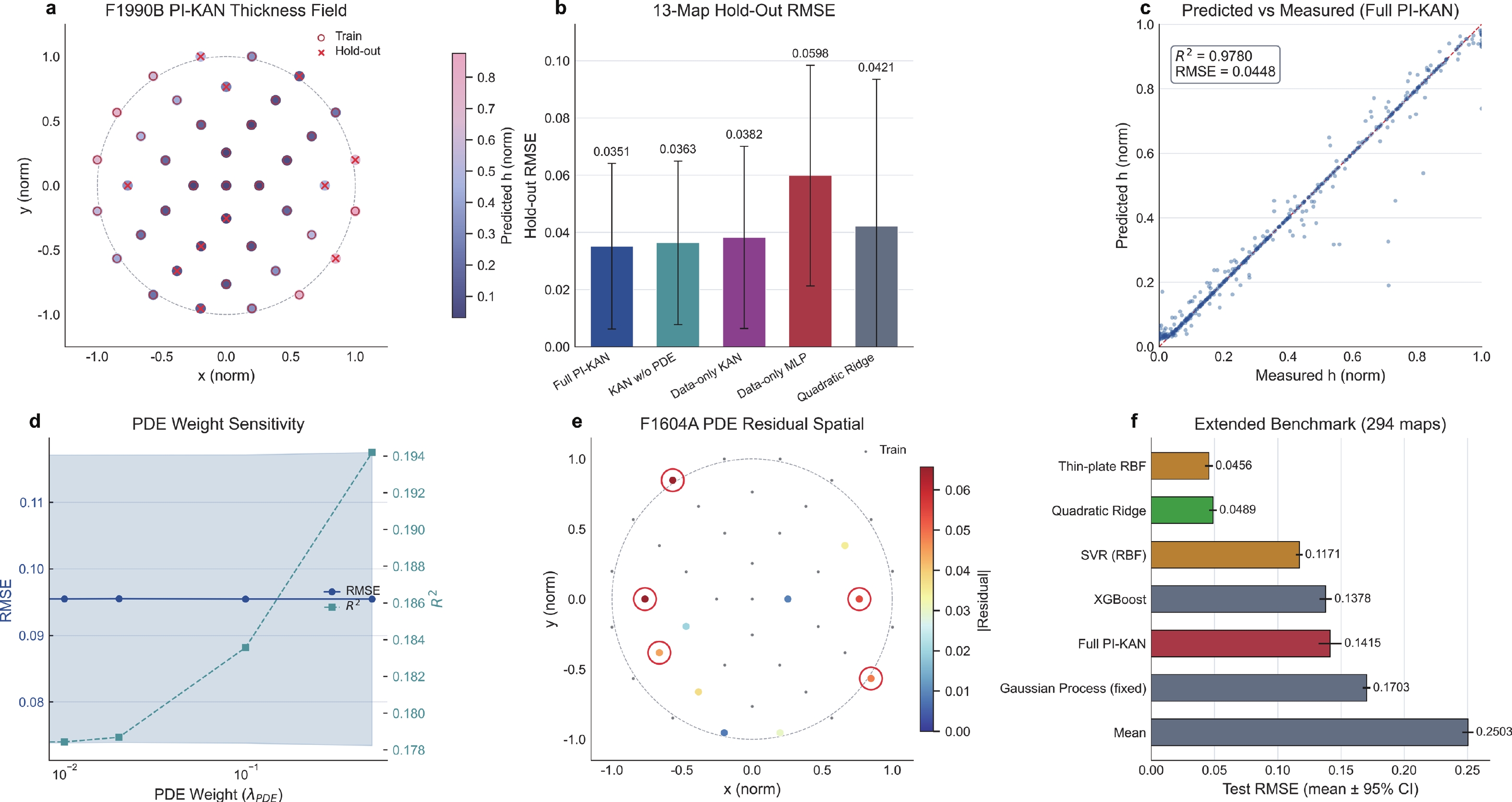
Fig. 6.  (Color online) PI-KAN spatial surrogate and benchmark comparison. (a) Reconstructed normalized thickness field on F1990B. (b) 13-map hold-out RMSE across PI-KAN variants and classical baselines. (c) Predicted vs. measured thickness with $ R^2 = 0.978 $. (d) PDE weight sensitivity analysis. (e) PDE residual spatial distribution on F1604A. (f) Unified benchmark ranking (top 6 methods) showing random-split and spatial-block RMSE.

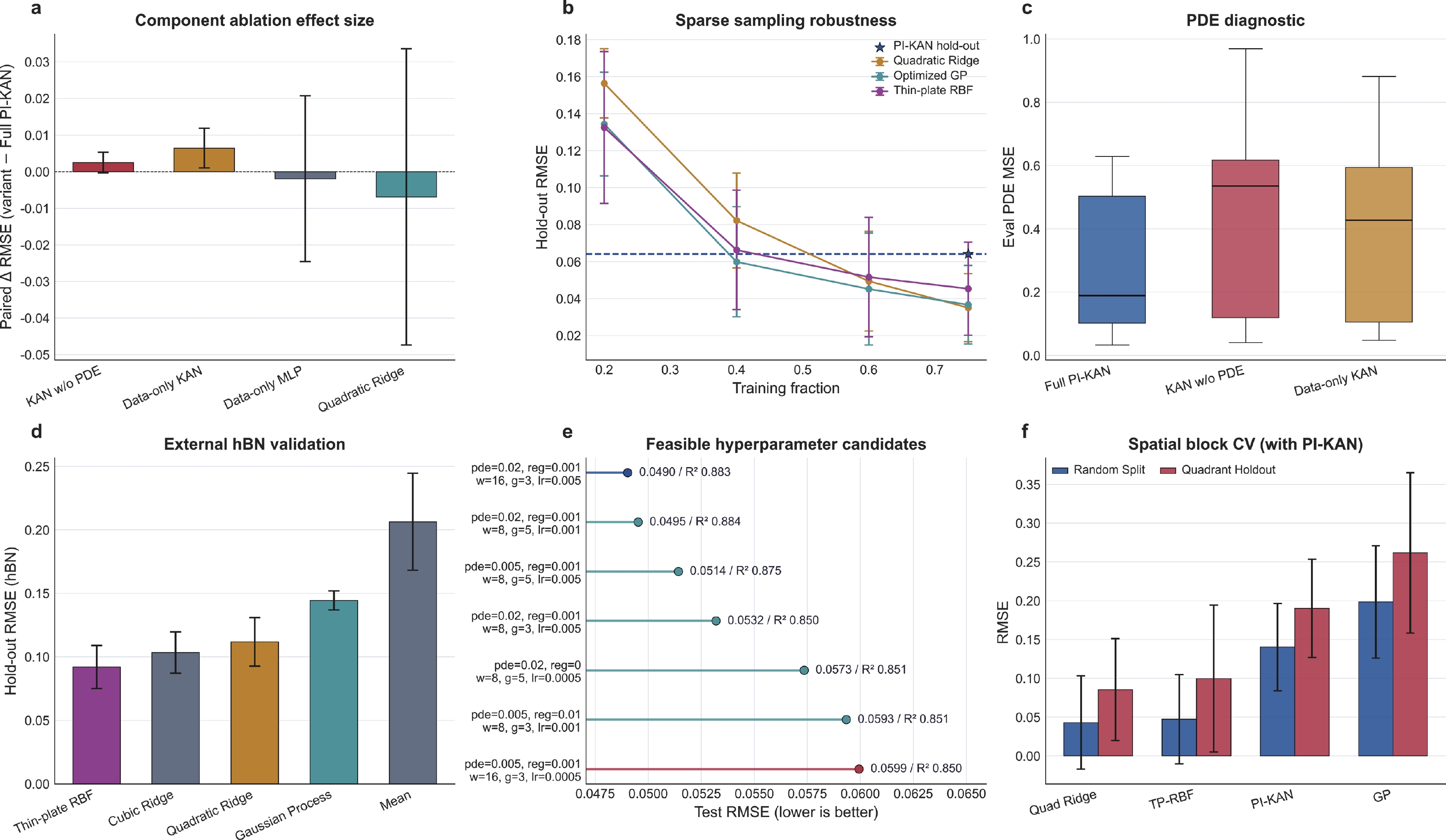
Fig. 7.  (Color online) PI-KAN validation and ablation. (a) Component ablation effect size: paired $ \Delta $RMSE for KAN w/o PDE, Data-only KAN, Data-only MLP, and Quadratic Ridge relative to full PI-KAN. (b) Sparse sampling robustness: hold-out RMSE vs. training fraction for PI-KAN and classical baselines. (c) PDE diagnostic: evaluation PDE residual MSE across PI-KAN variants. (d) External hBN validation: hold-out RMSE across methods on 6 hBN wafer maps. (e) Hyperparameter feasible region: best vs. worst RMSE across PDE weight, regularization, width, grid size, and learning rate. (f) Spatial-block cross-validation extrapolation: random-split vs. quadrant-holdout RMSE.

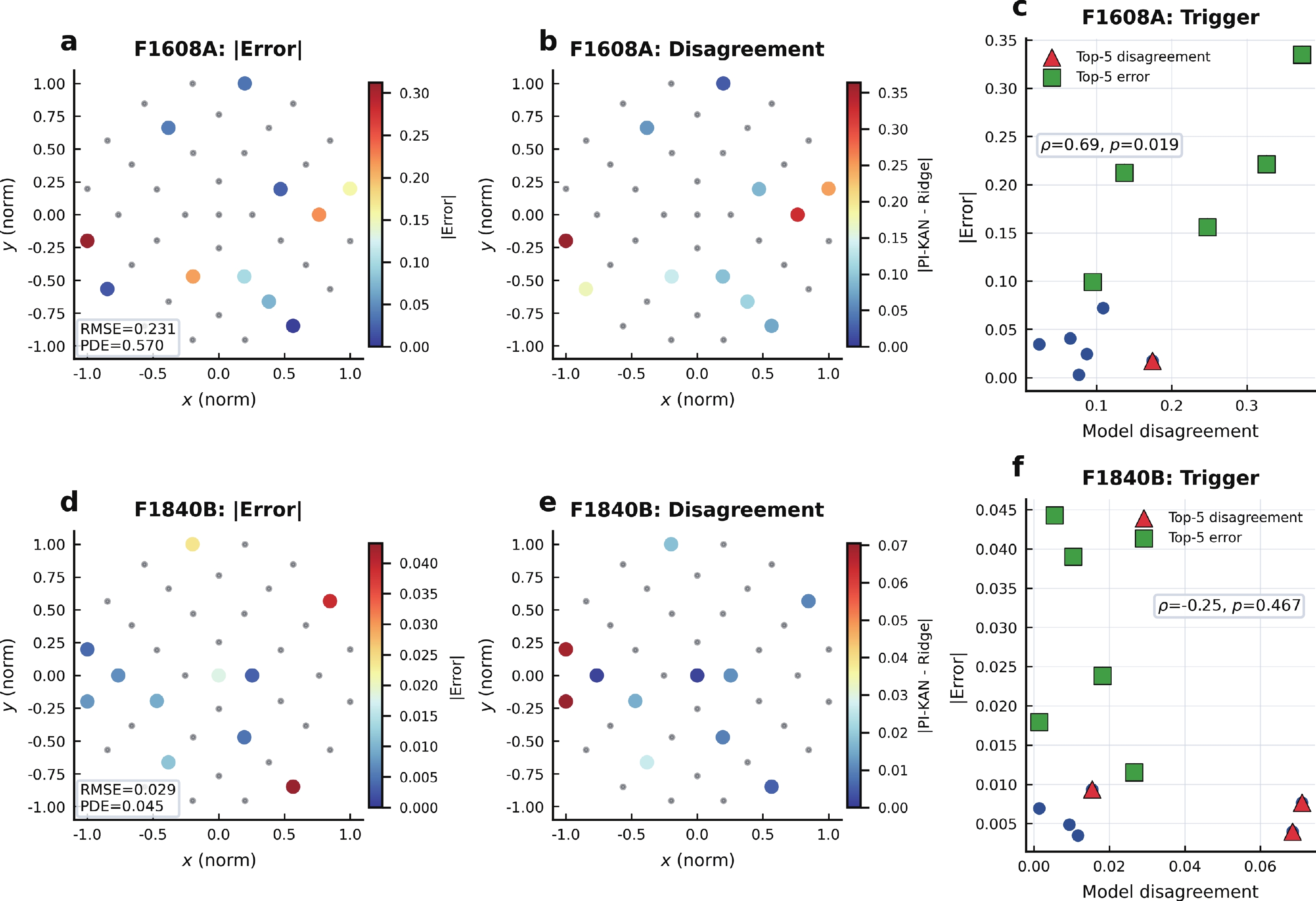
Fig. 8.  (Color online) Diagnostic case study: F1608A (high-error, top row) vs. F1840B (low-error, bottom row). (a,d) Spatial distribution of absolute prediction error at held-out test points (train points shown as black dots). (b,e) Spatial distribution of model disagreement (|PI-KAN - Ridge|). (c,f) Scatter of absolute error vs. disagreement with top-5 trigger points marked ($ \triangle $: top-5 disagreement; $ \square $: top-5 error). F1608A shows strong disagreement–error correlation ($ \rho = 0.691 $, $ p = 0.019 $); F1840B shows no significant correlation ($ \rho = -0.245 $, $ p = 0.467 $).

Table 1.   Datasets and validation roles.

DatasetSamplesMeasured quantityRole
Zenodo MOVPE/AlN F1990B41 spatial pointsFilmetrics thickness mapMOCVD flux-field validation
Zenodo MOVPE/AlN (13 maps)533 points (13 $ \times $ 41)Filmetrics thickness mapsPI-KAN LOOCV and cross-wafer transfer
Zenodo MOVPE/AlN augmented4,264 points (104 maps)Geometric transforms of 13 mapsPI-KAN extended benchmark
Zenodo hBN (6 maps)2,340 pointsEllipsometry thickness mapsPI-KAN out-of-distribution validation
OpenMV silicon wafer184 wafers (9 sites)G1–G9 nine-site thicknessPR/XGBoost prediction and MBE distribution
OpenMV interpolated7,544 points (184 $ \times $ 41)Thin-plate spline interpolated mapsPI-KAN extended benchmark
DownLoad: CSV

Table 3.   Source-stratified extended benchmark RMSE by data origin. ``Measured'' sources (MOVPE-orig, hBN) use directly observed thickness points; ``Interpolated'' sources (OpenMV) use thin-plate-spline-derived 41-point grids. Thin-plate RBF is marked with $ \dagger $ to indicate that it shares the kernel family used for OpenMV interpolation.

SourceTypeThin-plate RBF$ ^\dagger $Quadratic RidgeSVR (RBF)XGBoost
MOVPE-orig (13 maps)Measured0.03940.04490.10410.1089
hBN (6 maps)Measured0.08690.10960.10230.1202
OpenMV (184 maps)Interpolated0.04780.04910.12490.1546
All (294 maps)Mixed0.04560.04890.11710.1378
DownLoad: CSV

Table 5.   Task-specific rankings for methods evaluated on all six dimensions under a common protocol (rank 1 = best within each column). SVR, LightGBM, and PI-KAN variants are excluded from this table because they were not evaluated on the robustness modules; their random-split accuracy ranks are reported in Table 4.

MethodRandom-split$ ^{a} $Spatial block$ ^{b} $Noise robust.$ ^{c} $Few-shot ($ n{=}10 $)Extended (294 maps)Extended (MOVPE-orig)
Thin-plate RBF123111
Quadratic Ridge214222
Gaussian Process441444
XGBoost332333
$ ^{a} $13-map MOVPE LOOCV.
$ ^{b} $Quadrant holdout.
$ ^{c} $RMSE-vs-$ \sigma $ slope.
DownLoad: CSV

Table 2.   PI-KAN value boundary. PI-KAN is used as a diagnostic overlay, not as the routine accuracy winner.

Value dimensionBest signalEvidenceInterpretation
Routine accuracyClassical baselinesQuadratic Ridge/Gaussian Process score 25 vs. full PI-KAN score 67Use baselines for release
Hybrid overlayHybrid QR+PI-KANMean RMSE ties QR (0.0449); wins on 7/13 mapsSelected-map gain
Standalone PI-KANQuadratic RidgePure PI-KAN wins on 0/13 maps against QRNo default replacement
Structured holdoutGP/PI-KANQuadrant penalty 31.9/35.5%; ring penalty 46.7%, but absolute RMSE remains worseRisk signal
Weak-PDE residualFull PI-KANResidual drops by 0.1040 vs. KAN w/o PDE and 0.0814 vs. data-only KANDiagnostic map
PDE residual–errorFull PI-KANMap-level PDE residual vs. test RMSE: $ \rho=0.698 $, $ p=0.008 $; point-level weak ($ \rho=0.086 $)Map-level diagnostic
Disagreement triggerHybrid QR+PI-KANTop-3 recall 0.385 vs. 0.273 random (lift 1.41$ \times $); 10/13 maps above randomAdd-measurement trigger
Model disagreementHybrid QR+PI-KANDisagreement correlates with held-out error ($ \rho=0.418 $, $ p=2.07 \times 10^{-7} $)Trigger added sites
DownLoad: CSV

Table 4.   Unified benchmark ranking (11 methods). Lower protocol-summary score is better. Noise slope and extrapolation penalty were evaluated for the top-4 classical/tree methods; neural methods are ranked by the feasible accuracy and hold-out modules only.

Rank Method Protocol score Random RMSE Noise slope Extrapolation penalty
1 Quadratic Ridge 25 0.0421 0.625 0.985
1 Gaussian Process 25 0.1729 0.112 0.712
3 Thin-plate RBF 26 0.0394 0.573 1.110
4 XGBoost 28 0.1089 0.116 0.547
5 LightGBM 57 0.2441
5 SVR (RBF) 57 0.0790
7 PI-KAN (full) 67 0.0641
8 KAN w/o PDE 68 0.0666
9 Data-only KAN 69 0.0706
10 Data-only MLP 72 0.0622
DownLoad: CSV
[1]
Hite J K. A review of homoepitaxy of III-nitride semiconductors by metal organic chemical vapor deposition and the effects on vertical devices. Crystals, 2023, 13(3): 387 doi: 10.3390/cryst13030387
[2]
Li X H, Xu Q, Zhang Z Y. Molecular beam epitaxy growth of quantum wires and quantum dots. Nanomaterials, 2023, 13(6): 960 [PubMed]
[3]
Wang B, Zeng Y G, Song Y, et al. Principles of selective area epitaxy and applications in III–V semiconductor lasers using MOCVD: A review. Crystals, 2022, 12(7): 1011. doi: 10.3390/cryst12071011
[4]
Lan X, Cheng Y L, Yang X D, et al. Wafer-scale engineering of two-dimensional transition metal dichalcogenides. Chip, 2023, 2(3): 100057 doi: 10.1016/j.chip.2023.100057
[5]
Liu Z J, Gong X G, Cheng J R, et al. Wafer-scale synthesis of two-dimensional materials for integrated electronics. Chip, 2024, 3(1): 100080 doi: 10.1016/j.chip.2023.100080
[6]
Gallagher J C, Mastro M A, Ebrish M A, et al. Using machine learning with optical profilometry for GaN wafer screening. Sci Rep, 2023, 13: 3352 doi: 10.1038/s41598-023-29107-9
[7]
Miller W, Schulz T, Lymperakis L, et al. Kinetic Monte Carlo simulations for AlN and AlGaN epitaxial growth on AlN. J Cryst Growth, 2023, 607: 127125 doi: 10.1016/j.jcrysgro.2023.127125
[8]
Li Y, Chen X, Ai W. Kinetic Monte Carlo simulation study of the early stages of epitaxial SiC (0001) growth. J Cryst Growth, 2023, 617: 127291 doi: 10.1016/j.jcrysgro.2023.127291
[9]
Momeni K, Ji Y, Nayir N, et al. A computational framework for guiding the MOCVD-growth of wafer-scale 2D materials. npj Comput Mater, 2022, 8: 240 doi: 10.1038/s41524-022-00936-y
[10]
He Y, Wang J, Luo T, et al. Analysis and optimization of MOCVD flow ratio based on machine learning and PSO algorithm. J Cryst Growth, 2022, 590: 126683 doi: 10.1016/j.jcrysgro.2022.126683
[11]
Lee J, Jin J. A novel method to design and evaluate artificial neural network for thin film thickness measurement traceable to the length standard. Sci Rep, 2022, 12: 2212 doi: 10.1038/s41598-022-06247-y
[12]
Shen C, Zhan W, Pan S, et al. Real-time self-optimization of quantum dot laser emissions during machine learning-assisted epitaxy. Adv Sci, 2025, 12(27): 2503059 doi: 10.1002/advs.202503059
[13]
Kapoor S, Narayanan A. Leakage and the reproducibility crisis in machine-learning-based science. Patterns, 2023, 4(9): 100804 doi: 10.1016/j.patter.2023.100804
[14]
Merchant A, Batzner S, Schoenholz S S, et al. Scaling deep learning for materials discovery. Nature, 2023, 624(7990): 80 doi: 10.1038/s41586-023-06735-9
[15]
Hirtz J, Li H, Zhao X, et al. TCAD augmented machine learning for semiconductor device failure troubleshooting and reverse engineering. J Semicond, 2021, 42(12): 124102
[16]
Cheng B, Wang Y, Wang C, et al. Computer vision based in-situ TEM image analysis by using features of shallow neural network. J Semicond, 2022, 43(8): 081001 doi: 10.1088/1674-4926/43/8/081001
[17]
Lei M, Pan S, Hao D, et al. Defect control of photoresist etch-back process based on plasma parameters. J Semicond, 2026, 47(3): 032401 doi: 10.1088/1674-4926/25090008
[18]
Liu D Y, Xu L M, Lin X M, et al. Machine learning for semiconductors. Chip, 2022, 1(4): 100033 doi: 10.1016/j.chip.2022.100033
[19]
Zhao X Z, Li A, Zhang J M, et al. Programmable photonics-empowered ultralow-cost photonic device metrology. Chip, 2026: 100200
[20]
Pampili P, Pristovsek M. Nitrogen-polar growth of AlN on vicinal (0001) sapphire by MOVPE. J Appl Phys, 2024, 135(19): 195303 doi: 10.1063/5.0202746
[21]
Sobolá I M. Global sensitivity indices for nonlinear mathematical models and their Monte Carlo estimates. Math Comput Simul, 2001, 55(1/2/3): 271
[22]
Herman J, Usher W. SALib: An open-source Python library for sensitivity analysis. J Open Source Softw, 2017, 2(9): 97 doi: 10.21105/joss.00097
[23]
To T B T, Almeida R, Ferreira S O, et al. Roughness and correlations in the transition from island to film growth: Simulations and application to CdTe deposition. Appl Surf Sci, 2021, 560: 149946 doi: 10.1016/j.apsusc.2021.149946
[24]
Peyré G, Cuturi M. Computational optimal transport with applications to data sciences. Found Trends® Mach Learn, 2019, 11(5/6): 355
[25]
Irandoukht A. Optimum ridge regression parameter using R-squared of prediction as a criterion for regression analysis. J Stat Theory Appl, 2021, 20(2): 242
[26]
Chen T Q, Guestrin C. XGBoost: A scalable tree boosting system. Proceedings of the 22nd ACM SIGKDD International Conference on Knowledge Discovery and Data Mining. San Francisco California USA. ACM, 2016: 785
[27]
Sagi O, Rokach L. Approximating XGBoost with an interpretable decision tree. Inf Sci, 2021, 572: 522 doi: 10.1016/j.ins.2021.05.055
[28]
Bentéjac C, Csörgő A, Martínez-Muñoz G. A comparative analysis of gradient boosting algorithms. Artif Intell Rev, 2021, 54(3): 1937 doi: 10.1007/s10462-020-09896-5
[29]
Ke G, Meng Q, Finley T, et al. LightGBM: A highly efficient gradient boosting decision tree. Advances in Neural Information Processing Systems, 2017: 3146
[30]
Kane V E. Process capability indices. J Qual Technol, 1986, 18(1): 41 doi: 10.1080/00224065.1986.11978984
[31]
Liu Z, Wang Y, Vaidya S, et al. KAN: Kolmogorov-Arnold networks. The Thirteenth International Conference on Learning Representations, 2025(补充卷期页码)
[32]
Zhang X Y, Zhou H J. Generalization bounds and model complexity for Kolmogorov-Arnold networks. 2024: arXiv: 2410.08026. https://arxiv.org/abs/2410.08026
[33]
Raissi M, Perdikaris P, Karniadakis G E. Physics-informed neural networks: A deep learning framework for solving forward and inverse problems involving nonlinear partial differential equations. J Comput Phys, 2019, 378: 686 doi: 10.1016/j.jcp.2018.10.045
  • Search

    Advanced Search >>

    GET CITATION

    shu

    Export: BibTex EndNote

    Article Metrics

    Article views: 3 Times PDF downloads: 0 Times Cited by: 0 Times

    History

    Received: Revised: Online: Accepted Manuscript: 17 September 2026

    Catalog

      Email This Article

      User name:
      Email:*请输入正确邮箱
      Code:*验证码错误
      Hua Zhang, Yingtao Guo, Longhua Liu, Zhigang Song, Wanhua Zheng. Sparse wafer metrology for semiconductor process control with physics-informed diagnostics[J]. Journal of Semiconductors, 2026, In Press. doi: 10.1088/1674-4926/26070009 ****H Zhang, Y T Guo, L H Liu, Z G Song, and W H Zheng, Sparse wafer metrology for semiconductor process control with physics-informed diagnostics[J]. J. Semicond., 2026, accepted doi: 10.1088/1674-4926/26070009
      Citation:
      Hua Zhang, Yingtao Guo, Longhua Liu, Zhigang Song, Wanhua Zheng. Sparse wafer metrology for semiconductor process control with physics-informed diagnostics[J]. Journal of Semiconductors, 2026, In Press. doi: 10.1088/1674-4926/26070009 ****
      H Zhang, Y T Guo, L H Liu, Z G Song, and W H Zheng, Sparse wafer metrology for semiconductor process control with physics-informed diagnostics[J]. J. Semicond., 2026, accepted doi: 10.1088/1674-4926/26070009

      Sparse wafer metrology for semiconductor process control with physics-informed diagnostics

      DOI: 10.1088/1674-4926/26070009
      CSTR: 32376.14.1674-4926.26070009
      More Information
      • Hua Zhang received his bachelor's degree from Zhejiang University of Technology in 2021. He is currently pursuing a master's degree at the University of Chinese Academy of Sciences under the supervision of Researcher Zhigang Song at the Institute of Semiconductors, Chinese Academy of Sciences. His research focuses on machine-learning-assisted modeling and diagnostics for MOCVD growth, including sparse wafer metrology, wafer-thickness prediction, and physics-informed simulation for semiconductor process control
      • Zhigang Song received his PhD degree in 2017 from the Institute of Semiconductors, Chinese Academy of Sciences (CAS), under the supervision of Academician Shushen Li. From 2017 to 2020, he conducted postdoctoral research at the Max Planck Institute for Chemical Physics of Solids in Germany and Nanyang Technological University in Singapore. In October 2020, he joined the Institute of Semiconductors, CAS, as an associate professor. His research interests include the simulation of semiconductor optoelectronic materials and device systems, AI and optoelectronic large models, and semiconductor photoelectric detection and sensing systems
      • Corresponding author: songzhigang@semi.ac.cnwhzheng@semi.ac.cn
      • Available Online: 2026-09-17

      Catalog

        /

        DownLoad:  Full-Size Img  PowerPoint
        Return
        Return