J. Semicond. >  Just Accepted

ARTICLES

Mitigation of substrate bias effect by front-side local Si removal in GaN-on-Si HEMTs

Yifan Yan1, 2, Ang Li1, 3, Guohao Yu1, 2, , Bohan Guo1, 2, Zhidong Wu1, 2, Runxian Xing1, Jiaan Zhou1, An Yang1, 2, Jinxia Jiang1, 2, Bosen Liu1, Yingfei Sun1, Wenkui Lin1, Zhongming Zeng1 and Baoshun Zhang1,

+ Author Affiliations

 Corresponding author: Guohao Yu, ghyu2009@sinano.ac.cn; Baoshun Zhang, bszhang2006@sinano.ac.cn

DOI: 10.1088/1674-4926/26070020CSTR: 32376.14.1674-4926.26070020

PDF

Turn off MathJax

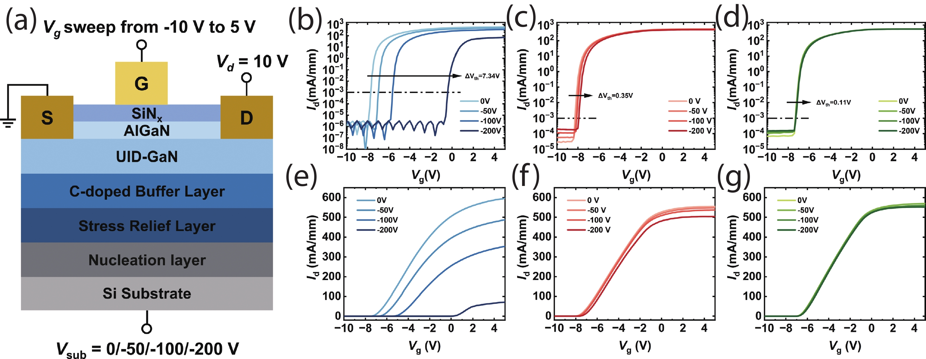
Abstract: GaN-on-Si HEMTs used for monolithic power integration suffer from substrate-bias-induced threshold-voltage shifts and saturation-current degradation. In this work, conventional, front-side local Si removed (FSR), and dielectric-filled FSR (Filled) devices are fabricated on the same commercial GaN-on-Si platform without backside-aligned processing. Under a substrate bias of -200 V, the conventional devices show a threshold-voltage (Vth) shift of 7.34 V and an 88% saturation-current (Isat) degradation, whereas the FSR and Filled devices show Vth shifts of 0.35 and 0.11 V with Isat degradations of 9% and 3%, respectively. Static and dynamic substrate-bias stress measurements further indicated reduced bias sensitivity of the FSR-based structures within the tested conditions. These results are consistent with the hypothesis that interrupting the local Si conduction path beneath the active region can mitigate substrate-bias-induced degradation.

Keywords: GaN-on-Si, substrate-bias effect, front-side local Si removal


[1]
Chen K J, Häberlen O, Lidow A, et al. GaN-on-Si power technology: Devices and applications. IEEE Trans Electron Devices, 2017, 64(3): 779 doi: 10.1109/TED.2017.2657579
[2]
Wei J, Zheng Z Y, Tang G F, et al. GaN power integration technology and its future prospects. IEEE Trans Electron Devices, 2024, 71(3): 1365 doi: 10.1109/TED.2023.3341053
[3]
Han Z F, Li X D, Ji J, et al. P-GaN gate HEMTs on 6-inch sapphire by CMOS-compatible process: A promising game changer for power electronics. IEEE Electron Device Lett, 2024, 45(7): 1257 doi: 10.1109/LED.2024.3401114
[4]
Udabe A, Baraia-Etxaburu I, Diez D G. Gallium nitride power devices: A state of the art review. IEEE Access, 2023, 11: 48628 doi: 10.1109/ACCESS.2023.3277200
[5]
Kim N, Yu J S, Zhang W J, et al. Current trends in the development of normally-OFF GaN-on-Si power transistors and power modules: A review. J Electron Mater, 2020, 49(11): 6829 doi: 10.1007/s11664-020-08284-7
[6]
Yang S, Liu S H, Lu Y Y, et al. Trapping mechanisms in insulated-gate GaN power devices: Understanding and characterization techniques. Phys Status Solidi A, 2017, 214(3): 1600607 doi: 10.1002/pssa.201600607
[7]
Posthuma N E, You S, Stoffels S, et al. An industry-ready 200 mm p-GaN E-mode GaN-on-Si power technology. 2018 IEEE 30th International Symposium on Power Semiconductor Devices and ICs, 2018: 284
[8]
Tang C Y, Deng C K, Fu C, et al. Low contact resistivity of <10 ω·mm for Au-free ohmic contact on p-GaN/AlGaN/GaN. IEEE Electron Device Lett, 2025, 46(1): 24 doi: 10.1109/LED.2024.3497584
[9]
Weiss B, Reiner R, Polyakov V, et al. Substrate biasing effects in a high-voltage, monolithically-integrated half-bridge GaN-Chip. 2017 IEEE 5th Workshop on Wide Bandgap Power Devices and Applications, 2017: 265
[10]
Jiang Q M, Tang Z K, Zhou C H, et al. Substrate-coupled cross-talk effects on an AlGaN/GaN-on-Si smart power IC platform. IEEE Trans Electron Devices, 2014, 61(11): 3808 doi: 10.1109/TED.2014.2355834
[11]
Yang J J, Wei J, Wang M J, et al. TCAD study on suppression of substrate-induced degradation in GaN-on-Si integrated half-bridge circuit by local Si lateral etch. IEEE Trans Electron Devices, 2023, 70(11): 5584 doi: 10.1109/TED.2023.3311411
[12]
Yang S, Zhou C H, Han S W, et al. Impact of substrate bias polarity on buffer-related current collapse in AlGaN/GaN-on-Si power devices. IEEE Trans Electron Devices, 2017, 64(12): 5048 doi: 10.1109/TED.2017.2764527
[13]
Yang S, Han S W, Sheng K, et al. Dynamic on-resistance in GaN power devices: Mechanisms, characterizations, and modeling. IEEE J Emerg Sel Top Power Electron, 2019, 7(3): 1425 doi: 10.1109/JESTPE.2019.2925117
[14]
Yang J X, Lin D J, Wu Y R, et al. Deep source metal trenches in GaN-on-Si HEMTs for relieving current collapse. IEEE J Electron Devices Soc, 2021, 9: 557 doi: 10.1109/JEDS.2021.3078522
[15]
Cosnier T, Syshchyk O, De Jaeger B, et al. 200 V GaN-on-SOI smart power platform for monolithic GaN power ICs. 2021 IEEE International Electron Devices Meeting, 2022: 5.1. 1
[16]
Li X D, Van Hove M, Zhao M, et al. 200 V enhancement-mode p-GaN HEMTs fabricated on 200 mm GaN-on-SOI with trench isolation for monolithic integration. IEEE Electron Device Lett, 2017, 38(7): 918 doi: 10.1109/LED.2017.2703304
[17]
Chandrasekar H, Uren M J, Eblabla A, et al. Buffer-induced current collapse in GaN HEMTs on highly resistive Si substrates. IEEE Electron Device Lett, 2018, 39(10): 1556 doi: 10.1109/LED.2018.2864562
[18]
Gonçalez Filho W, Borga M, Geens K, et al. Development and analysis of thick GaN drift layers on 200 mm CTE-matched substrate for vertical device processing. Sci Rep, 2023, 13: 15931 doi: 10.1038/s41598-023-42747-1
[19]
Wei J, Zhang M, Lyu G, et al. GaN integrated bridge circuits on bulk silicon substrate: Issues and proposed solution. IEEE J Electron Devices Soc, 2021, 9: 545 doi: 10.1109/JEDS.2021.3077273
[20]
Lyu G, Wei J, Song W J, et al. A GaN power integration platform based on engineered bulk Si substrate with eliminated crosstalk between high-side and low-side HEMTs. 2021 IEEE International Electron Devices Meeting, 2022: 5.2. 1
[21]
Abid I, Canato E, Meneghini M, et al. GaN-on-silicon transistors with reduced current collapse and improved blocking voltage by means of local substrate removal. Appl Phys Express, 2021, 14(3): 036501 doi: 10.35848/1882-0786/abdca0
[22]
Chen Y T, Huang J. Current collapse suppression in AlGaN/GaN HEMTs using silicon substrate removal technique. 2019 IEEE Workshop on Wide Bandgap Power Devices and Applications in Asia (WiPDA Asia), 2019: 1
[23]
Lin Y, Chiu Y S, Chang E Y. Investigation of p-GaN Gate HEMT using Removal Si Substrate and part of Buffer Layer. 2022 IET International Conference on Engineering Technologies and Applications (IET-ICETA), 2022: 1
[24]
Srivastava P, Das J, Visalli D, et al. Silicon substrate removal of GaN DHFETs for enhanced (<1100 V) breakdown voltage. IEEE Electron Device Lett, 2010, 31(8): 851 doi: 10.1109/LED.2010.2050673
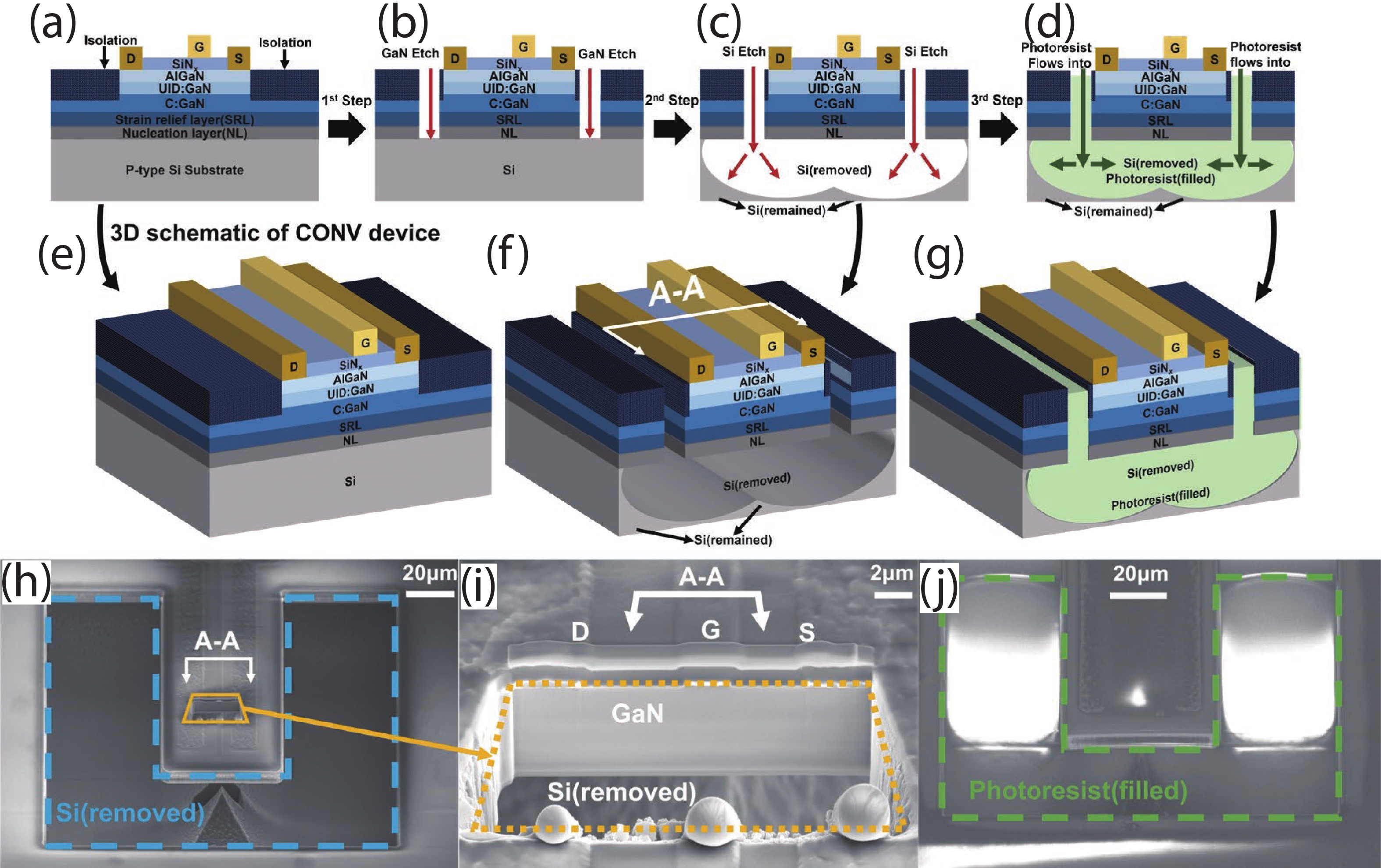
Fig. 1.  (Color online) Side views of the fabricated front-side local Si substrate removal structures with large device size. (a)-(d) Plan view of the FSR structures’ fabrication process, (e) 3D schematic of CONV devices, (f) 3D schematic of FSR devices, (g) 3D schematic of Filled devices. (h)(i) SEM microstructure micrograph of FSR devices, bule region is the area of removed Si substrate, yellow region is the cross-sectional FIB-micrograph of devices. (j)SEM microstructure micrograph of Filled devices, green region is the photoresist filled region.

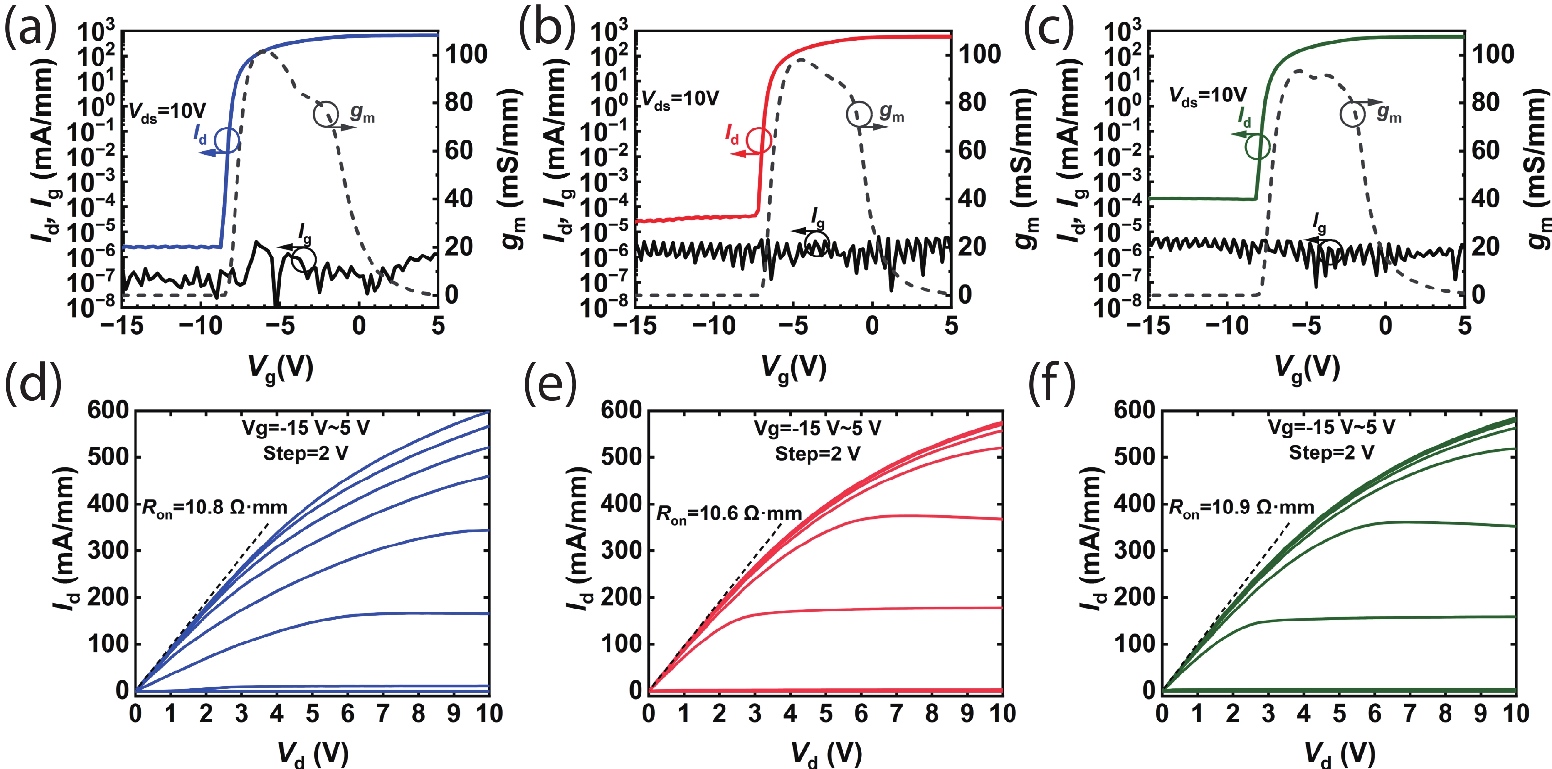
Fig. 2.  (Color online) Transfer and output characteristics of the CONV, FSR, and Filled devices. The top panels show the transfer characteristics, and the bottom panels show the output characteristics. The CONV, FSR, and Filled devices are represented by blue, red, and green curves, respectively.

Fig. 3.  (Color online) Measurement configuration and transfer characteristics of the devices. (a) Schematic cross-section of the device structure and biasing scheme used for the transfer measurements, where Vg was swept from –10 to 5 V at Vd = 10 V under substrate biases of Vsub = 0, –50, –100 and –200 V. (b–d) Semi-logarithmic and (e–g) linear-scale transfer characteristics of the CONV, FSR, and Filled devices, respectively. The CONV, FSR, and Filled devices are represented by blue, red, and green curves, respectively. The extracted threshold-voltage shifts (ΔVth) are indicated in the corresponding semi-logarithmic plots.

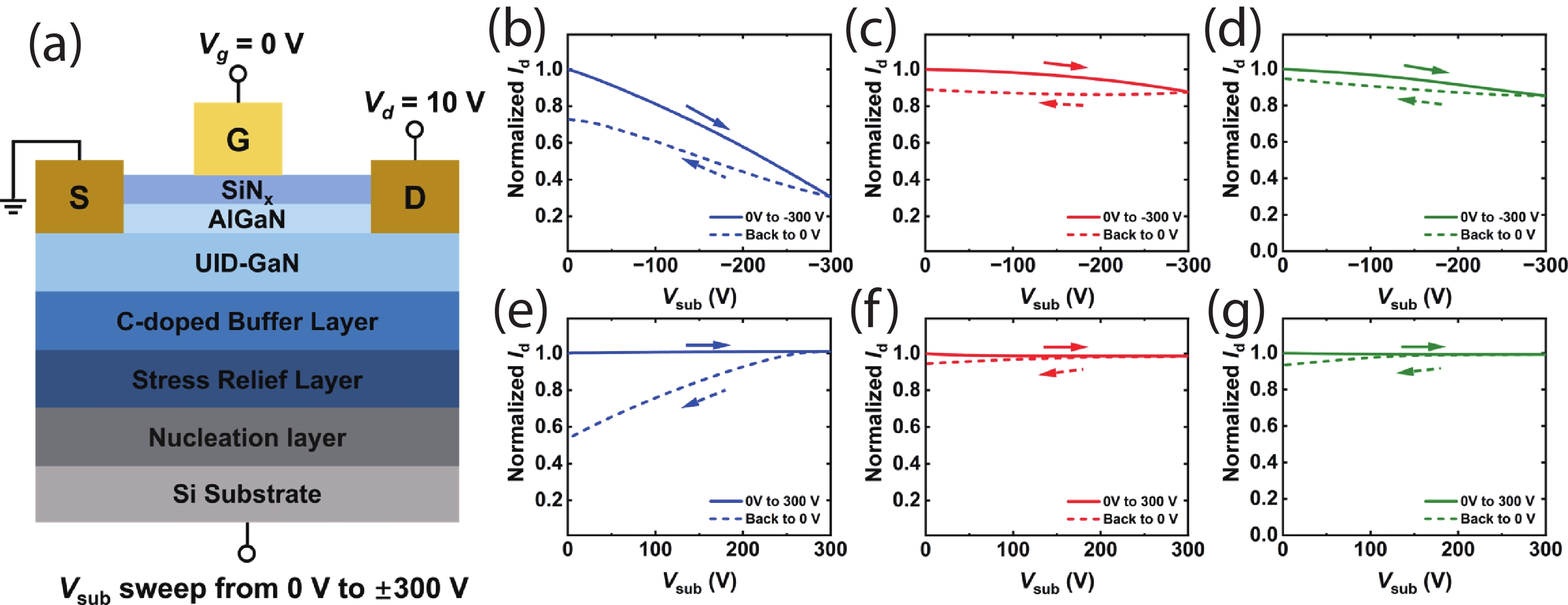
Fig. 4.  (Color online) Substrate-bias sweeping characteristics of the CONV, FSR, and Filled devices. (a) Device schematic and measurement configuration with Vg = 0 V, Vd = 10 V and Vsub swept from 0 to ±300 V. (b–d) Normalized Id responses during negative Vsub sweeping from 0 to –300 V and back to 0 V for the CONV, FSR, and Filled devices, respectively. (e–g) Normalized Id responses during positive Vsub sweeping from 0 to 300 V and back to 0 V for the corresponding devices. Solid lines denote the forward sweep, and dashed lines denote the return sweep.

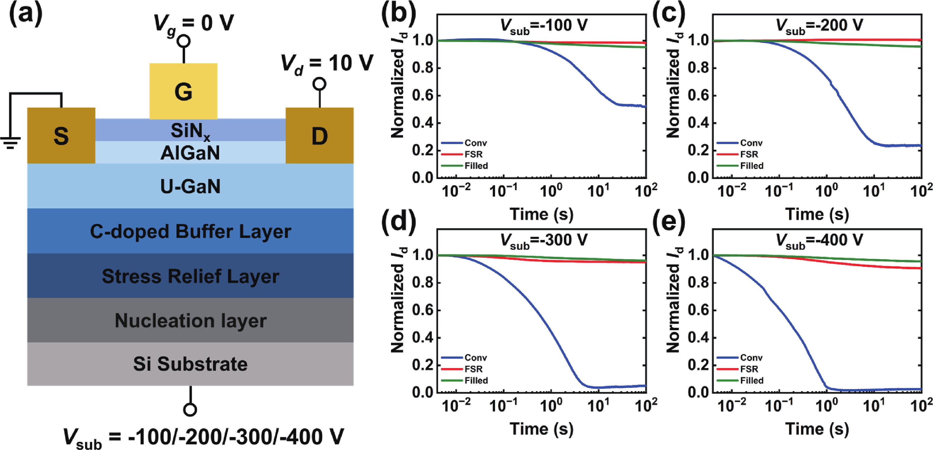
Fig. 5.  (Color online) Time-dependent drain-current stability under negative substrate-bias stress. (a) Schematic cross-section of the device structure and measurement configuration with Vg = 0 V, Vd = 10 V and Vsub = –100, –200, –300, and –400 V. (b–e) Time evolution of the normalized Id for the CONV, FSR, and Filled devices, respectively. The blue, red, and green curves correspond to the CONV, FSR, and Filled devices, respectively.

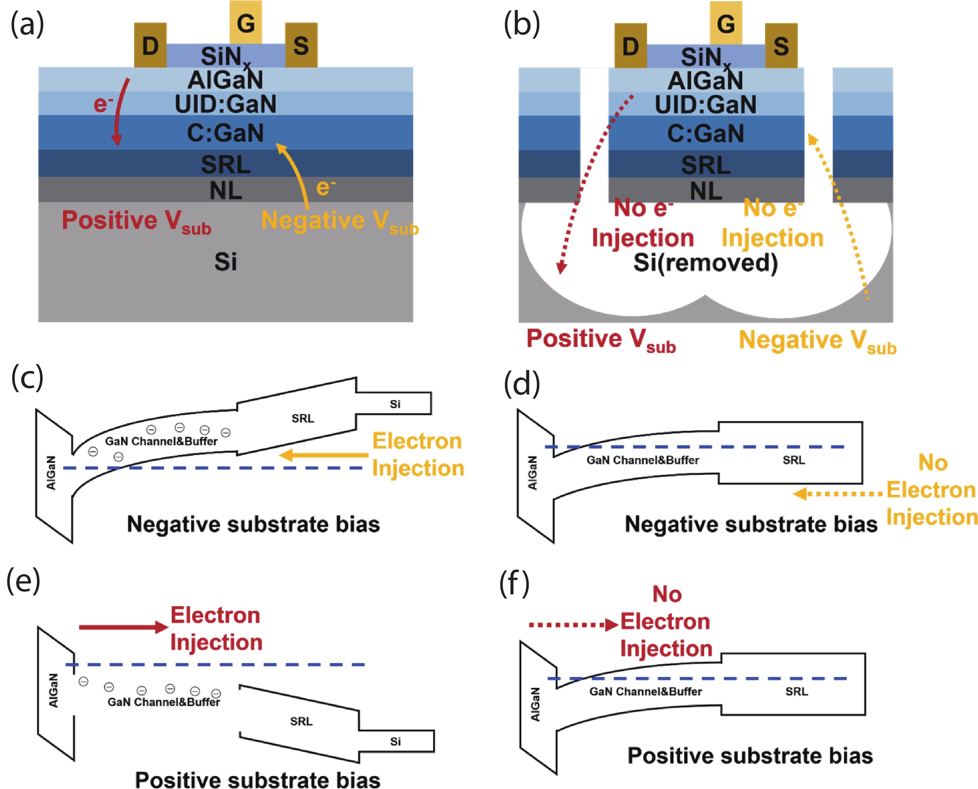
Fig. 6.  (Color online) Schematic cross-sections and qualitative energy-band diagrams illustrating the influence of Si substrate removal on substrate bias induced carrier transport. CONV structure with Si substrate (a) and FSR-based structures with Si substrate removal (b), respectively. (c, d) Corresponding band diagrams under negative substrate bias. (e, f) Corresponding band diagrams under positive substrate bias. The band profiles are qualitative and not drawn to scale.

[1]
Chen K J, Häberlen O, Lidow A, et al. GaN-on-Si power technology: Devices and applications. IEEE Trans Electron Devices, 2017, 64(3): 779 doi: 10.1109/TED.2017.2657579
[2]
Wei J, Zheng Z Y, Tang G F, et al. GaN power integration technology and its future prospects. IEEE Trans Electron Devices, 2024, 71(3): 1365 doi: 10.1109/TED.2023.3341053
[3]
Han Z F, Li X D, Ji J, et al. P-GaN gate HEMTs on 6-inch sapphire by CMOS-compatible process: A promising game changer for power electronics. IEEE Electron Device Lett, 2024, 45(7): 1257 doi: 10.1109/LED.2024.3401114
[4]
Udabe A, Baraia-Etxaburu I, Diez D G. Gallium nitride power devices: A state of the art review. IEEE Access, 2023, 11: 48628 doi: 10.1109/ACCESS.2023.3277200
[5]
Kim N, Yu J S, Zhang W J, et al. Current trends in the development of normally-OFF GaN-on-Si power transistors and power modules: A review. J Electron Mater, 2020, 49(11): 6829 doi: 10.1007/s11664-020-08284-7
[6]
Yang S, Liu S H, Lu Y Y, et al. Trapping mechanisms in insulated-gate GaN power devices: Understanding and characterization techniques. Phys Status Solidi A, 2017, 214(3): 1600607 doi: 10.1002/pssa.201600607
[7]
Posthuma N E, You S, Stoffels S, et al. An industry-ready 200 mm p-GaN E-mode GaN-on-Si power technology. 2018 IEEE 30th International Symposium on Power Semiconductor Devices and ICs, 2018: 284
[8]
Tang C Y, Deng C K, Fu C, et al. Low contact resistivity of <10 ω·mm for Au-free ohmic contact on p-GaN/AlGaN/GaN. IEEE Electron Device Lett, 2025, 46(1): 24 doi: 10.1109/LED.2024.3497584
[9]
Weiss B, Reiner R, Polyakov V, et al. Substrate biasing effects in a high-voltage, monolithically-integrated half-bridge GaN-Chip. 2017 IEEE 5th Workshop on Wide Bandgap Power Devices and Applications, 2017: 265
[10]
Jiang Q M, Tang Z K, Zhou C H, et al. Substrate-coupled cross-talk effects on an AlGaN/GaN-on-Si smart power IC platform. IEEE Trans Electron Devices, 2014, 61(11): 3808 doi: 10.1109/TED.2014.2355834
[11]
Yang J J, Wei J, Wang M J, et al. TCAD study on suppression of substrate-induced degradation in GaN-on-Si integrated half-bridge circuit by local Si lateral etch. IEEE Trans Electron Devices, 2023, 70(11): 5584 doi: 10.1109/TED.2023.3311411
[12]
Yang S, Zhou C H, Han S W, et al. Impact of substrate bias polarity on buffer-related current collapse in AlGaN/GaN-on-Si power devices. IEEE Trans Electron Devices, 2017, 64(12): 5048 doi: 10.1109/TED.2017.2764527
[13]
Yang S, Han S W, Sheng K, et al. Dynamic on-resistance in GaN power devices: Mechanisms, characterizations, and modeling. IEEE J Emerg Sel Top Power Electron, 2019, 7(3): 1425 doi: 10.1109/JESTPE.2019.2925117
[14]
Yang J X, Lin D J, Wu Y R, et al. Deep source metal trenches in GaN-on-Si HEMTs for relieving current collapse. IEEE J Electron Devices Soc, 2021, 9: 557 doi: 10.1109/JEDS.2021.3078522
[15]
Cosnier T, Syshchyk O, De Jaeger B, et al. 200 V GaN-on-SOI smart power platform for monolithic GaN power ICs. 2021 IEEE International Electron Devices Meeting, 2022: 5.1. 1
[16]
Li X D, Van Hove M, Zhao M, et al. 200 V enhancement-mode p-GaN HEMTs fabricated on 200 mm GaN-on-SOI with trench isolation for monolithic integration. IEEE Electron Device Lett, 2017, 38(7): 918 doi: 10.1109/LED.2017.2703304
[17]
Chandrasekar H, Uren M J, Eblabla A, et al. Buffer-induced current collapse in GaN HEMTs on highly resistive Si substrates. IEEE Electron Device Lett, 2018, 39(10): 1556 doi: 10.1109/LED.2018.2864562
[18]
Gonçalez Filho W, Borga M, Geens K, et al. Development and analysis of thick GaN drift layers on 200 mm CTE-matched substrate for vertical device processing. Sci Rep, 2023, 13: 15931 doi: 10.1038/s41598-023-42747-1
[19]
Wei J, Zhang M, Lyu G, et al. GaN integrated bridge circuits on bulk silicon substrate: Issues and proposed solution. IEEE J Electron Devices Soc, 2021, 9: 545 doi: 10.1109/JEDS.2021.3077273
[20]
Lyu G, Wei J, Song W J, et al. A GaN power integration platform based on engineered bulk Si substrate with eliminated crosstalk between high-side and low-side HEMTs. 2021 IEEE International Electron Devices Meeting, 2022: 5.2. 1
[21]
Abid I, Canato E, Meneghini M, et al. GaN-on-silicon transistors with reduced current collapse and improved blocking voltage by means of local substrate removal. Appl Phys Express, 2021, 14(3): 036501 doi: 10.35848/1882-0786/abdca0
[22]
Chen Y T, Huang J. Current collapse suppression in AlGaN/GaN HEMTs using silicon substrate removal technique. 2019 IEEE Workshop on Wide Bandgap Power Devices and Applications in Asia (WiPDA Asia), 2019: 1
[23]
Lin Y, Chiu Y S, Chang E Y. Investigation of p-GaN Gate HEMT using Removal Si Substrate and part of Buffer Layer. 2022 IET International Conference on Engineering Technologies and Applications (IET-ICETA), 2022: 1
[24]
Srivastava P, Das J, Visalli D, et al. Silicon substrate removal of GaN DHFETs for enhanced (<1100 V) breakdown voltage. IEEE Electron Device Lett, 2010, 31(8): 851 doi: 10.1109/LED.2010.2050673
  • Search

    Advanced Search >>

    GET CITATION

    shu

    Export: BibTex EndNote

    Article Metrics

    Article views: 3 Times PDF downloads: 0 Times Cited by: 0 Times

    History

    Received: 10 July 2026 Revised: 25 August 2026 Online: Accepted Manuscript: 28 September 2026

    Catalog

      Email This Article

      User name:
      Email:*请输入正确邮箱
      Code:*验证码错误
      Yifan Yan, Ang Li, Guohao Yu, Bohan Guo, Zhidong Wu, Runxian Xing, Jiaan Zhou, An Yang, Jinxia Jiang, Bosen Liu, Yingfei Sun, Wenkui Lin, Zhongming Zeng, Baoshun Zhang. Mitigation of substrate bias effect by front-side local Si removal in GaN-on-Si HEMTs[J]. Journal of Semiconductors, 2026, In Press. doi: 10.1088/1674-4926/26070020 ****Y F Yan, A Li, G H Yu, B H Guo, Z D Wu, R X Xing, J A Zhou, A Yang, J X Jiang, B S Liu, Y F Sun, W K Lin, Z M Zeng, and B S Zhang, Mitigation of substrate bias effect by front-side local Si removal in GaN-on-Si HEMTs[J]. J. Semicond., 2026, accepted doi: 10.1088/1674-4926/26070020
      Citation:
      Yifan Yan, Ang Li, Guohao Yu, Bohan Guo, Zhidong Wu, Runxian Xing, Jiaan Zhou, An Yang, Jinxia Jiang, Bosen Liu, Yingfei Sun, Wenkui Lin, Zhongming Zeng, Baoshun Zhang. Mitigation of substrate bias effect by front-side local Si removal in GaN-on-Si HEMTs[J]. Journal of Semiconductors, 2026, In Press. doi: 10.1088/1674-4926/26070020 ****
      Y F Yan, A Li, G H Yu, B H Guo, Z D Wu, R X Xing, J A Zhou, A Yang, J X Jiang, B S Liu, Y F Sun, W K Lin, Z M Zeng, and B S Zhang, Mitigation of substrate bias effect by front-side local Si removal in GaN-on-Si HEMTs[J]. J. Semicond., 2026, accepted doi: 10.1088/1674-4926/26070020

      Mitigation of substrate bias effect by front-side local Si removal in GaN-on-Si HEMTs

      DOI: 10.1088/1674-4926/26070020
      CSTR: 32376.14.1674-4926.26070020
      More Information
      • Yifan Yan received his BS degree in 2023 from Southwest Jiaotong University. Now he is a doctoral student at University of Science and Technology of China under the supervision of Research Fellow Baoshun Zhang. His research focuses on GaN power electronic devices and GaN power conversion modules
      • Guohao Yu received his PhD in Microelectronics and Solid-State Electronics from the Suzhou Institute of Nano-Tech and Nano-Bionics (SINANO), Chinese Academy of Sciences in 2013. He then conducted postdoctoral research at SINANO and currently serves as a Senior Engineer at the institute. His research interests focus on GaN power electronic devices and GaN power conversion modules
      • Baoshun Zhang received his BS degree from Changchun University of Science and Technology in 1994 and his PhD degree from the Institute of Semiconductors, Chinese Academy of Sciences in 2003. Then he joined in Hong Kong University of Science and Technology. Currently, he is a Research Fellow at Suzhou Institute of Nano-Tech and Nano-Bionics, Chinese Academy of Sciences, and his research interests include semiconductor material growth and device technology research
      • Corresponding author: ghyu2009@sinano.ac.cn; bszhang2006@sinano.ac.cn
      • Received Date: 2026-07-10
      • Revised Date: 2026-08-25
      • Available Online: 2026-09-28

      Catalog

        /

        DownLoad:  Full-Size Img  PowerPoint
        Return
        Return