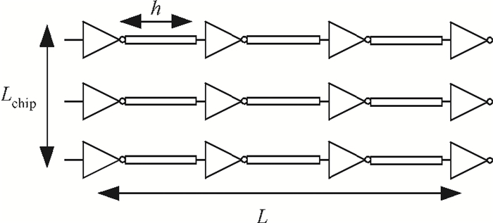
Fig. 1.
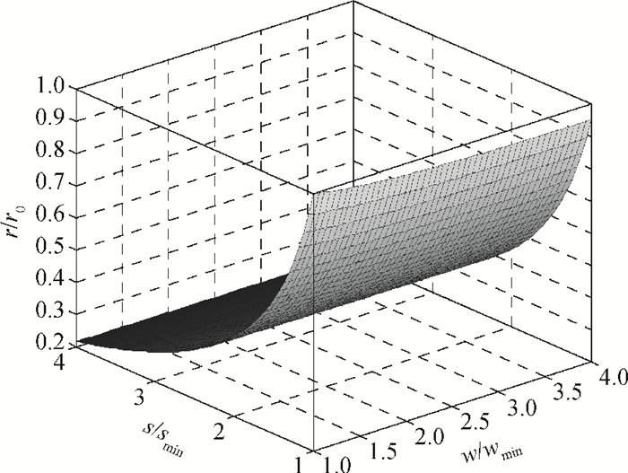
The variation of $r$ with $w$ and $s$ .
SEMICONDUCTOR INTEGRATED CIRCUITS
Yan Zhang, Gang Dong, Yintang Yang, Ning Wang, Yaoshun Ding, Xiaoxian Liu and Fengjuan Wang
Corresponding author: Zhang Yan, zylap@aliyun.com
Abstract: Considering the self-heating effect, an accurate expression for the global interconnection resistance per unit length in terms of interconnection wire width and spacing is presented. Based on the proposed resistance model and according to the trade-off theory, a novel optimization analytical model of delay, power dissipation and bandwidth is derived. The proposed optimal model is verified and compared based on 90 nm, 65 nm and 40 nm CMOS technologies. It can be found that more optimum results can be easily obtained by the proposed model. This optimization model is more accurate and realistic than the conventional optimization models, and can be integrated into the global interconnection design of nano-scale integrated circuits.
Keywords: self-heating effect, interconnection wire resistance per unit length, optimal model, very large scale integration
| [1] |
Semiconductor Industry Association 2012 International Technology Roadmap for Semiconductors 2012(ITRS 2012)
|
| [2] |
Chen G Q, Friedman E G. Low-power repeaters driving RC and RLC interconnects with delay and bandwidth constraints. IEEE Trans Very Large Scale Integr Syst, 2006, 14(2):161 doi: 10.1109/TVLSI.2005.863750
|
| [3] |
Abinash R, Chowdhury M H. Global interconnect optimization in the presence of on-chip inductance. IEEE International Symposium on Circuits and Systems, 2007:885 http://ieeexplore.ieee.org/document/4252777/?arnumber=4252777&contentType=Conference%20Publications
|
| [4] |
Faiz-ul-Hassan, Fernando R, Vanderbauwhede W A. Optimization of on-chip link performance under area, power and variability constraints. 22nd International Conference on Microelectronics, 2010:48 http://ieeexplore.ieee.org/document/5696196/?arnumber=5696196&punumber%3D5686267
|
| [5] |
Zhu Z M, Wan D J, Yang Y T. An interconnect width and spacing optimization model considering scattering effect. Chin Phys B, 2010, 19(9):097803 doi: 10.1088/1674-1056/19/9/097803
|
| [6] |
Vinita V D, Jeffrey A D. Optimal voltage scaling, repeater insertion, and wire sizing for wave-pipelined global interconnects. IEEE Trans Circuits Syst Ⅰ:Fundamental Theory and Applications, 2008, 55(4):1023 doi: 10.1109/TCSI.2008.916506
|
| [7] |
Tang M, Mao J F. Wire sizing optimization for buffered global interconnects. International Conference on Microwave and Millimeter Wave Technology, 2008:431 http://ieeexplore.ieee.org/document/4540430/
|
| [8] |
Zhu Z M, Zhong B, He B T. A novel nanometer CMOS interconnect optimal model with target delay and bandwidth constraint. Acta Phys Sin, 2010, 59(3):1997
|
| [9] |
Ashok N, Ramalingam S. Variability aware low-power delay optimal buffer insertion for global interconnects. IEEE Trans Circuits Syst Ⅰ, Reg Pap, 2010, 57(12):3055 doi: 10.1109/TCSI.2010.2073790
|
| [10] |
Fargol H, Nasser M. Interconnect sizing and spacing with consideration of buffer insertion for simultaneous crosstalk-delay optimization. IEEE International Conference on Design and Test of Integrated Systems in Nanoscale Era, 2008:12008 http://ieeexplore.ieee.org/document/4540218/keywords
|
| [11] |
Renatas J, Friedman E G. Resource based optimization for simultaneous shield and repeater insertion. IEEE Trans Very Large Scale Integr Syst, 2010, 18(5):742 doi: 10.1109/TVLSI.2009.2015950
|
| [12] |
Mahmoud Z, Nasser M. Throughput optimization for interleaved repeater-inserted interconnects in VLSI design. IEEE 3rd International Nanoelectronics Conference, 2010:1 http://ieeexplore.ieee.org/document/5424802/?reload=true&arnumber=5424802&punumber%3D5416830
|
| [13] |
Houman Z, Asim A, Yvon S. Repeater insertion in power-managed VLSI systems. Proc ACM Great Lakes Symp VLSI GLSVLSI, 2011:395 http://dblp.uni-trier.de/db/conf/glvlsi/glvlsi2011.html
|
| [14] |
Massimo A, Stephane B, Yusuf L. Optimization of the wire grid size for differential routing:analysis and impact on the power-delay-area tradeoff. Microelectron J, 2010, 41:669 doi: 10.1016/j.mejo.2010.06.005
|
| [15] |
Sandeep S A, Mahesh K, Sreehari V. An Alternative approach to buffer insertion for delay and power reduction in VLSI interconnects. 23rd International Conference on VLSI Design, 2010:441 http://ieeexplore.ieee.org/document/5401211/?arnumber=5401211
|
| [16] |
Zhu Z M, Wan D J, Yang Y T. An optimization model of wire size for multi-objective constrain. Acta Phys Sin, 2009, 59(7):4838 http://d.wanfangdata.com.cn/Periodical_wlxb201007067.aspx
|
| [17] |
Liu J, Dong G, Xue M, et al. Performance optimization of global interconnect based on dual supply and dual threshold voltages. Acta Phys Sin, 2012, 60(4):046602
|
| [18] |
Zhu Z M, Qian L B, Yang Y T, et al. A novel interconnect-optimal repeater insertion model with a target delay constraint. Journal of Semiconductors, 2008, 20(4):1847 http://www.jos.ac.cn/bdtxbcn/ch/reader/view_abstract.aspx?file_no=08010601&flag=1
|
| [19] |
Banafsheh B Y K, Joshi S K. Interconnect joule heating under transient currents using the transmission line matrix method. J Electron Packaging, 2012, 139:011009 http://electronicpackaging.asmedigitalcollection.asme.org/article.aspx?articleid=1410141&resultClick=1
|
| [20] |
Yokogawa S, Kakuhara Y, Tsuchiya H. Joule heating effects on electromigration in Cu/low-k interconnects. IEEE International Reliability Physics Symposium Proceedings, 2009:837
|
| [21] |
Ni M, Memik S O M. Self-heating aware optimal wire sizing under Elmore delay model. Proc Des Autom Test Eur. DATE Nice Acropolis, 2007:1373 http://ieeexplore.ieee.org/document/4211999/
|
| [22] |
Ajami A H, Banerjee K, Pedram M. Modeling and analysis of nonuniform substrate temperature effects on global ULSI interconnects. IEEE Trans Comput Aided Des Integr Circuits Syst, 2005, 24(6):849 doi: 10.1109/TCAD.2005.847944
|
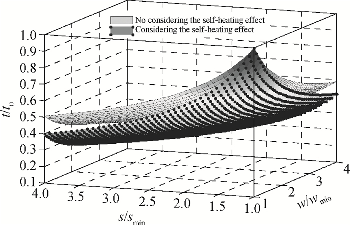
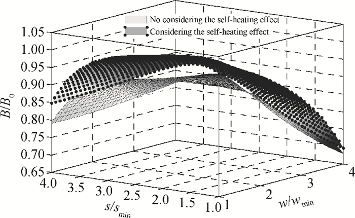
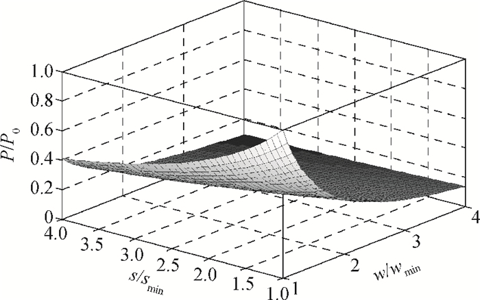
Table 1. The interconnection wire processing parameter and electric parameter of 40 nm[1].

|
Table 2. The interconnection parameters at 90 nm, 65 nm and 40nm CMOS technologies[1].

|
Table 3. Comparison of interconnect dimension parameters between two kinds of optimization results.

|
Table 4. Comparison of interconnect delay, power dissipation and bandwidth between two kinds of optimization results.

|
| [1] |
Semiconductor Industry Association 2012 International Technology Roadmap for Semiconductors 2012(ITRS 2012)
|
| [2] |
Chen G Q, Friedman E G. Low-power repeaters driving RC and RLC interconnects with delay and bandwidth constraints. IEEE Trans Very Large Scale Integr Syst, 2006, 14(2):161 doi: 10.1109/TVLSI.2005.863750
|
| [3] |
Abinash R, Chowdhury M H. Global interconnect optimization in the presence of on-chip inductance. IEEE International Symposium on Circuits and Systems, 2007:885 http://ieeexplore.ieee.org/document/4252777/?arnumber=4252777&contentType=Conference%20Publications
|
| [4] |
Faiz-ul-Hassan, Fernando R, Vanderbauwhede W A. Optimization of on-chip link performance under area, power and variability constraints. 22nd International Conference on Microelectronics, 2010:48 http://ieeexplore.ieee.org/document/5696196/?arnumber=5696196&punumber%3D5686267
|
| [5] |
Zhu Z M, Wan D J, Yang Y T. An interconnect width and spacing optimization model considering scattering effect. Chin Phys B, 2010, 19(9):097803 doi: 10.1088/1674-1056/19/9/097803
|
| [6] |
Vinita V D, Jeffrey A D. Optimal voltage scaling, repeater insertion, and wire sizing for wave-pipelined global interconnects. IEEE Trans Circuits Syst Ⅰ:Fundamental Theory and Applications, 2008, 55(4):1023 doi: 10.1109/TCSI.2008.916506
|
| [7] |
Tang M, Mao J F. Wire sizing optimization for buffered global interconnects. International Conference on Microwave and Millimeter Wave Technology, 2008:431 http://ieeexplore.ieee.org/document/4540430/
|
| [8] |
Zhu Z M, Zhong B, He B T. A novel nanometer CMOS interconnect optimal model with target delay and bandwidth constraint. Acta Phys Sin, 2010, 59(3):1997
|
| [9] |
Ashok N, Ramalingam S. Variability aware low-power delay optimal buffer insertion for global interconnects. IEEE Trans Circuits Syst Ⅰ, Reg Pap, 2010, 57(12):3055 doi: 10.1109/TCSI.2010.2073790
|
| [10] |
Fargol H, Nasser M. Interconnect sizing and spacing with consideration of buffer insertion for simultaneous crosstalk-delay optimization. IEEE International Conference on Design and Test of Integrated Systems in Nanoscale Era, 2008:12008 http://ieeexplore.ieee.org/document/4540218/keywords
|
| [11] |
Renatas J, Friedman E G. Resource based optimization for simultaneous shield and repeater insertion. IEEE Trans Very Large Scale Integr Syst, 2010, 18(5):742 doi: 10.1109/TVLSI.2009.2015950
|
| [12] |
Mahmoud Z, Nasser M. Throughput optimization for interleaved repeater-inserted interconnects in VLSI design. IEEE 3rd International Nanoelectronics Conference, 2010:1 http://ieeexplore.ieee.org/document/5424802/?reload=true&arnumber=5424802&punumber%3D5416830
|
| [13] |
Houman Z, Asim A, Yvon S. Repeater insertion in power-managed VLSI systems. Proc ACM Great Lakes Symp VLSI GLSVLSI, 2011:395 http://dblp.uni-trier.de/db/conf/glvlsi/glvlsi2011.html
|
| [14] |
Massimo A, Stephane B, Yusuf L. Optimization of the wire grid size for differential routing:analysis and impact on the power-delay-area tradeoff. Microelectron J, 2010, 41:669 doi: 10.1016/j.mejo.2010.06.005
|
| [15] |
Sandeep S A, Mahesh K, Sreehari V. An Alternative approach to buffer insertion for delay and power reduction in VLSI interconnects. 23rd International Conference on VLSI Design, 2010:441 http://ieeexplore.ieee.org/document/5401211/?arnumber=5401211
|
| [16] |
Zhu Z M, Wan D J, Yang Y T. An optimization model of wire size for multi-objective constrain. Acta Phys Sin, 2009, 59(7):4838 http://d.wanfangdata.com.cn/Periodical_wlxb201007067.aspx
|
| [17] |
Liu J, Dong G, Xue M, et al. Performance optimization of global interconnect based on dual supply and dual threshold voltages. Acta Phys Sin, 2012, 60(4):046602
|
| [18] |
Zhu Z M, Qian L B, Yang Y T, et al. A novel interconnect-optimal repeater insertion model with a target delay constraint. Journal of Semiconductors, 2008, 20(4):1847 http://www.jos.ac.cn/bdtxbcn/ch/reader/view_abstract.aspx?file_no=08010601&flag=1
|
| [19] |
Banafsheh B Y K, Joshi S K. Interconnect joule heating under transient currents using the transmission line matrix method. J Electron Packaging, 2012, 139:011009 http://electronicpackaging.asmedigitalcollection.asme.org/article.aspx?articleid=1410141&resultClick=1
|
| [20] |
Yokogawa S, Kakuhara Y, Tsuchiya H. Joule heating effects on electromigration in Cu/low-k interconnects. IEEE International Reliability Physics Symposium Proceedings, 2009:837
|
| [21] |
Ni M, Memik S O M. Self-heating aware optimal wire sizing under Elmore delay model. Proc Des Autom Test Eur. DATE Nice Acropolis, 2007:1373 http://ieeexplore.ieee.org/document/4211999/
|
| [22] |
Ajami A H, Banerjee K, Pedram M. Modeling and analysis of nonuniform substrate temperature effects on global ULSI interconnects. IEEE Trans Comput Aided Des Integr Circuits Syst, 2005, 24(6):849 doi: 10.1109/TCAD.2005.847944
|


Article views: 2956 Times PDF downloads: 14 Times Cited by: 0 Times
Received: 29 March 2013 Revised: 09 June 2013 Online: Published: 01 November 2013
| Citation: |
Yan Zhang, Gang Dong, Yintang Yang, Ning Wang, Yaoshun Ding, Xiaoxian Liu, Fengjuan Wang. A novel interconnect optimal buffer insertion model considering the self-heating effect[J]. Journal of Semiconductors, 2013, 34(11): 115004. doi: 10.1088/1674-4926/34/11/115004
****
Y Zhang, G Dong, Y T Yang, N Wang, Y S Ding, X X Liu, F J Wang. A novel interconnect optimal buffer insertion model considering the self-heating effect[J]. J. Semicond., 2013, 34(11): 115004. doi: 10.1088/1674-4926/34/11/115004.

|
| [1] |
Semiconductor Industry Association 2012 International Technology Roadmap for Semiconductors 2012(ITRS 2012)
|
| [2] |
Chen G Q, Friedman E G. Low-power repeaters driving RC and RLC interconnects with delay and bandwidth constraints. IEEE Trans Very Large Scale Integr Syst, 2006, 14(2):161 doi: 10.1109/TVLSI.2005.863750
|
| [3] |
Abinash R, Chowdhury M H. Global interconnect optimization in the presence of on-chip inductance. IEEE International Symposium on Circuits and Systems, 2007:885 http://ieeexplore.ieee.org/document/4252777/?arnumber=4252777&contentType=Conference%20Publications
|
| [4] |
Faiz-ul-Hassan, Fernando R, Vanderbauwhede W A. Optimization of on-chip link performance under area, power and variability constraints. 22nd International Conference on Microelectronics, 2010:48 http://ieeexplore.ieee.org/document/5696196/?arnumber=5696196&punumber%3D5686267
|
| [5] |
Zhu Z M, Wan D J, Yang Y T. An interconnect width and spacing optimization model considering scattering effect. Chin Phys B, 2010, 19(9):097803 doi: 10.1088/1674-1056/19/9/097803
|
| [6] |
Vinita V D, Jeffrey A D. Optimal voltage scaling, repeater insertion, and wire sizing for wave-pipelined global interconnects. IEEE Trans Circuits Syst Ⅰ:Fundamental Theory and Applications, 2008, 55(4):1023 doi: 10.1109/TCSI.2008.916506
|
| [7] |
Tang M, Mao J F. Wire sizing optimization for buffered global interconnects. International Conference on Microwave and Millimeter Wave Technology, 2008:431 http://ieeexplore.ieee.org/document/4540430/
|
| [8] |
Zhu Z M, Zhong B, He B T. A novel nanometer CMOS interconnect optimal model with target delay and bandwidth constraint. Acta Phys Sin, 2010, 59(3):1997
|
| [9] |
Ashok N, Ramalingam S. Variability aware low-power delay optimal buffer insertion for global interconnects. IEEE Trans Circuits Syst Ⅰ, Reg Pap, 2010, 57(12):3055 doi: 10.1109/TCSI.2010.2073790
|
| [10] |
Fargol H, Nasser M. Interconnect sizing and spacing with consideration of buffer insertion for simultaneous crosstalk-delay optimization. IEEE International Conference on Design and Test of Integrated Systems in Nanoscale Era, 2008:12008 http://ieeexplore.ieee.org/document/4540218/keywords
|
| [11] |
Renatas J, Friedman E G. Resource based optimization for simultaneous shield and repeater insertion. IEEE Trans Very Large Scale Integr Syst, 2010, 18(5):742 doi: 10.1109/TVLSI.2009.2015950
|
| [12] |
Mahmoud Z, Nasser M. Throughput optimization for interleaved repeater-inserted interconnects in VLSI design. IEEE 3rd International Nanoelectronics Conference, 2010:1 http://ieeexplore.ieee.org/document/5424802/?reload=true&arnumber=5424802&punumber%3D5416830
|
| [13] |
Houman Z, Asim A, Yvon S. Repeater insertion in power-managed VLSI systems. Proc ACM Great Lakes Symp VLSI GLSVLSI, 2011:395 http://dblp.uni-trier.de/db/conf/glvlsi/glvlsi2011.html
|
| [14] |
Massimo A, Stephane B, Yusuf L. Optimization of the wire grid size for differential routing:analysis and impact on the power-delay-area tradeoff. Microelectron J, 2010, 41:669 doi: 10.1016/j.mejo.2010.06.005
|
| [15] |
Sandeep S A, Mahesh K, Sreehari V. An Alternative approach to buffer insertion for delay and power reduction in VLSI interconnects. 23rd International Conference on VLSI Design, 2010:441 http://ieeexplore.ieee.org/document/5401211/?arnumber=5401211
|
| [16] |
Zhu Z M, Wan D J, Yang Y T. An optimization model of wire size for multi-objective constrain. Acta Phys Sin, 2009, 59(7):4838 http://d.wanfangdata.com.cn/Periodical_wlxb201007067.aspx
|
| [17] |
Liu J, Dong G, Xue M, et al. Performance optimization of global interconnect based on dual supply and dual threshold voltages. Acta Phys Sin, 2012, 60(4):046602
|
| [18] |
Zhu Z M, Qian L B, Yang Y T, et al. A novel interconnect-optimal repeater insertion model with a target delay constraint. Journal of Semiconductors, 2008, 20(4):1847 http://www.jos.ac.cn/bdtxbcn/ch/reader/view_abstract.aspx?file_no=08010601&flag=1
|
| [19] |
Banafsheh B Y K, Joshi S K. Interconnect joule heating under transient currents using the transmission line matrix method. J Electron Packaging, 2012, 139:011009 http://electronicpackaging.asmedigitalcollection.asme.org/article.aspx?articleid=1410141&resultClick=1
|
| [20] |
Yokogawa S, Kakuhara Y, Tsuchiya H. Joule heating effects on electromigration in Cu/low-k interconnects. IEEE International Reliability Physics Symposium Proceedings, 2009:837
|
| [21] |
Ni M, Memik S O M. Self-heating aware optimal wire sizing under Elmore delay model. Proc Des Autom Test Eur. DATE Nice Acropolis, 2007:1373 http://ieeexplore.ieee.org/document/4211999/
|
| [22] |
Ajami A H, Banerjee K, Pedram M. Modeling and analysis of nonuniform substrate temperature effects on global ULSI interconnects. IEEE Trans Comput Aided Des Integr Circuits Syst, 2005, 24(6):849 doi: 10.1109/TCAD.2005.847944
|

 WeChat ID
Journal of Semiconductors © 2017 All Rights Reserved 京ICP备05085259号-2

 DownLoad: