| [1] |
Trivedi V, Fossum J G, Chowdhury M M, et al. Nanoscale FinFETs with gate source drain underlap. IEEE Trans Electron Devices, 2005, 52(1):56 doi: 10.1109/TED.2004.841333 |
| [2] |
Kim S, Fossum J G, Yang J, et al. Modeling and significance of fringe capacitance in nonclassical CMOS devices with G-S/drain underlap. IEEE Trans Electron Devices, 2006, 53(9):5 http://ieeexplore.ieee.org/document/1677847/ |
| [3] |
Yang J W, Zeitzoff P M, Tseng H H, et al. Highly manufacturable double-gate FinFET with G-S/drain underlap. IEEE Trans Electron Devices, 2007, 54(6):1464 doi: 10.1109/TED.2007.896387 |
| [4] |
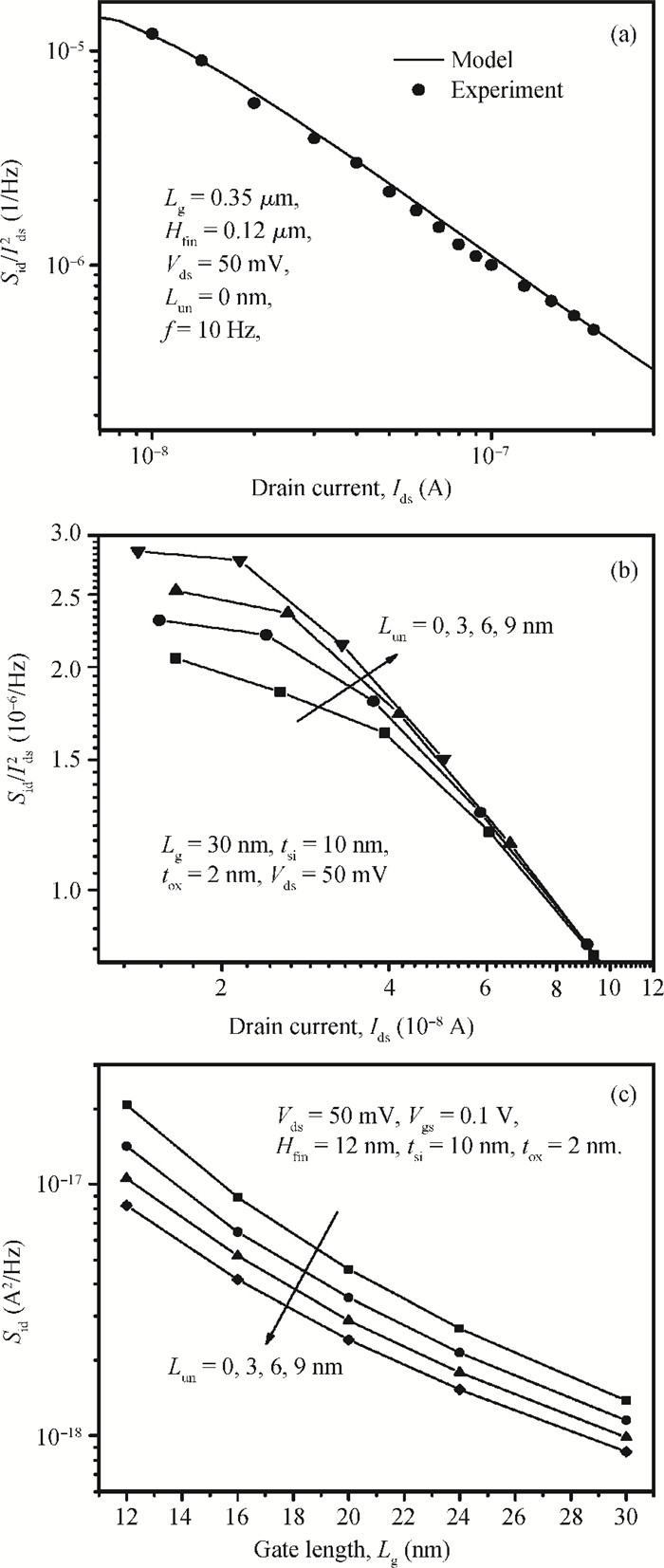
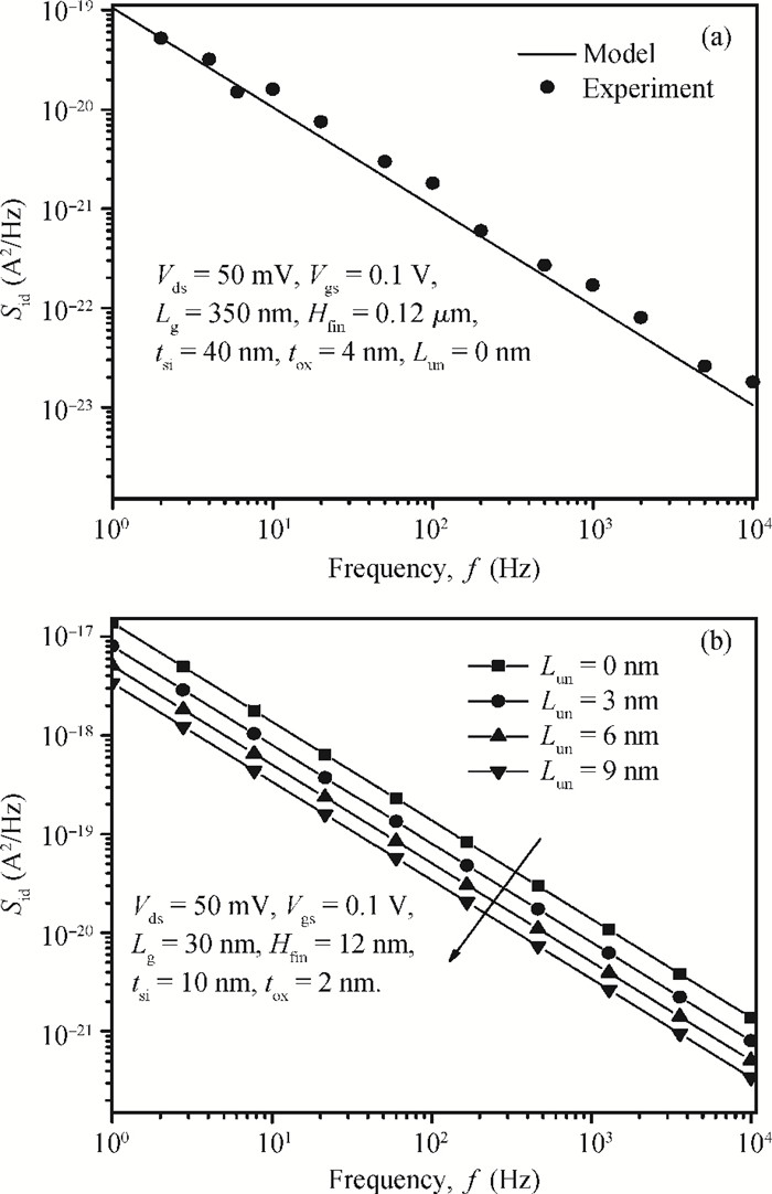
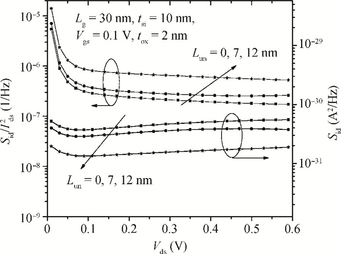
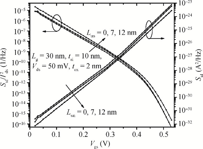
Pandit S, Syamal B, Sarkar C K, et al. Analytical modeling of flicker and thermal noise in n-channel DG FinFETs. Solid-State Electron, 2011, 63(1):177 doi: 10.1016/j.sse.2011.05.026 |
| [5] |
Hung K K, Ko P K, Hu C, et al. A unified model for the flicker noise in metal-oxide-semiconductor field-effect transistors. IEEE Trans Electron Devices, 1990, 37(3):654 doi: 10.1109/16.47770 |
| [6] |
Vandamme E P, Lode K, Vandamme J, et al. Critical discussion on unified 1/$f$ noise models for MOSFETs. IEEE Trans Electron Devices, 2000, 47(11):2146 doi: 10.1109/16.877177 |
| [7] |
Li Z, Ma J, Ye Y, et al. Compact channel noise models for deep-submicron MOSFETs. IEEE Trans Electron Devices, 2009, 56(6):1300 doi: 10.1109/TED.2009.2018160 |
| [8] |
|
| [9] |
|
| [10] |
|
| [11] |
Knoblinger G, Klein P, Tiebout M, et al. A new model for thermal channel noise of deep-submicron MOSFETS and its application in RF-CMOS design. IEEE J Solid-State Circuits, 2001, 36(5):831 doi: 10.1109/4.918922 |
| [12] |
Chen C H, Deen M J. Channel noise modeling of deep submicron MOSFETs. IEEE Trans Electron Devices, 2002, 49(8):1484 doi: 10.1109/TED.2002.801229 |
| [13] |
Teng H F, Jang S L, Juang M H, et al. A unified model for high-frequency current noise of MOSFETs. Solid-State Electron, 2003, 47(11):2043 doi: 10.1016/S0038-1101(03)00248-X |
| [14] |
Roy A S, Enz C C. Compact modeling of thermal noise in the MOS transistor. IEEE Trans Electron Devices, 2005, 52(4):611 doi: 10.1109/TED.2005.844735 |
| [15] |
Bansal A, Member S, Roy K, et al. Analytical subthreshold potential distribution model for gate underlap DG MOS transistors. IEEE Trans Electron Devices, 2007, 54(7):1793 doi: 10.1109/TED.2007.898042 |
| [16] |
Vaddi R, Agarwal R P, Dasgupta S, et al. Analytical modeling of subthreshold current and subthreshold swing of an underlap DGMOSFET with tied-independent gate and symmetric-asymmetric options. Microelectron J, 2011, 42(5):798 doi: 10.1016/j.mejo.2011.01.004 |
| [17] |
|
| [18] |
Dey A, Chakravorty A, Dasgupta N, et al. Analytical model of subthreshold current and slope for asymmetric 4-T and 3-T DG MOSFETs. IEEE Trans Electron Devices, 2008, 55(12):3442 doi: 10.1109/TED.2008.2006109 |
| [19] |
Moldovan O, Jiménez D, Guitart J R, et al. Explicit analytical charge and capacitance models of undoped DG MOSFETs. IEEE Trans Electron Devices, 2007, 54(7):1718 doi: 10.1109/TED.2007.899402 |
| [20] |
Roy A S, Enz C C, Sallese J M, et al. Noise modeling methodologies in the presence of mobility degradation and their equivalence. IEEE Trans Electron Devices, 2006, 53(2):348 doi: 10.1109/TED.2005.862703 |
| [21] |
Wei C, Xiong Y Z, Zhou X. Investigation of low-frequency noise in N-channel FinFETs from weak to strong inversion. IEEE Trans Electron Devices, 2009, 56(11):2800 doi: 10.1109/TED.2009.2030972 |
| [22] |
Chowdhury M M, Fossum J G. Physical insights on electron mobility in contemporary FinFETs. IEEE Trans Electron Devices, 2006, 27(6):482 doi: 10.1109/LED.2006.874214 |


 DownLoad: