


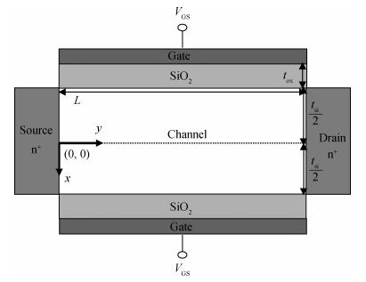
Fig. 1.
Schematic diagram of a DG MOSFET. $L$ , $t_{\rm si}$ and $t_{\rm ox}$ are the channel length, channel thickness and oxide thickness, respectively.
SEMICONDUCTOR DEVICES
Sarvesh Dubey1, Kumar Tiwari2 and S. Jit1,
Corresponding author: S. Jit, Email:sjit.ece@itbhu.ac.in
Abstract: An analytic drain current model is presented for doped short-channel double-gate MOSFETs with a Gaussian-like doping profile in the vertical direction of the channel. The present model is valid in linear and saturation regions of device operation. The drain current variation with various device parameters has been demonstrated. The model is made more physical by incorporating the channel length modulation effect. Parameters like transconductance and drain conductance that are important in assessing the analog performance of the device have also been formulated. The model results are validated by numerical simulation results obtained by using the commercially available ATLASTM, a two dimensional device simulator from SILVACO.
Keywords: drain current, DG MOSFET, transconductance, drain conductance
| [1] |
I. T. R. S. , 2008
|
| [2] |
Wong H S P. Beyond the conventional transistor. IBM J Res Devices, 2002, 46:133 doi: 10.1147/rd.462.0133
|
| [3] |
Wong H S P, Frank D J, Solomon P M. Device design considerations for double-gate, ground-plane, and single-gated ultra-thin SOI MOSFET's at the 25 nm channel length generation. IEDM Tech Dig, 1998:407
|
| [4] |
Kolberg S. Modeling of electrostatics and drain current in nanoscale double-gate MOSFETs. PhD Thesis, Norwegian University of Science and Technology, 2007
|
| [5] |
Suzuki K, Sugii T. Analytical models for n+-p+ double-gate SOI MOSFET's. IEEE Trans Electron Devices, 1995, 42:1940 doi: 10.1109/16.469401
|
| [6] |
Taur Y, Liang X, Wang W, et al. A continuous, analytic drain-current model for DG MOSFETs. IEEE Electron Device Lett, 2004, 25:107 doi: 10.1109/LED.2003.822661
|
| [7] |
Hariharan V, Vasi J, Rao V R. Drain current model including velocity saturation for symmetric double-gate MOSFETs. IEEE Trans Electron Devices, 2008, 55:2173 doi: 10.1109/TED.2008.926745
|
| [8] |
Reyboz M, Martin P, Poiroux T, et al. Continuous model for independent double gate MOSFET. Solid-State Electron, 2009, 53:504 doi: 10.1016/j.sse.2009.02.005
|
| [9] |
Mohammadi S, Afzali-Kusha A. Modeling of drain current, capacitance and transconductance in thin film undoped symmetric DG MOSFETs including quantum effects. Microelectron Reliab, 2010, 50:338 doi: 10.1016/j.microrel.2009.12.002
|
| [10] |
Ioannidis E G, Theodorou C G, Tsormpatzoglou A, et al. Analytical low-frequency noise model in the linear region of lightly doped nanoscale double-gate metal-oxide-semiconductor field-effect transistors. J Appl Phys, 2010, 108:064512 doi: 10.1063/1.3483279
|
| [11] |
Papathanasiou K, Theodorou C G, Tsormpatzoglou A, et al. Symmetrical unified compact model of short-channel double-gate MOSFETs. Solid-State Electron, 2012, 69:55 doi: 10.1016/j.sse.2011.10.002
|
| [12] |
Dubey S, Tiwari P K, Jit S. A two-dimensional model for the potential distribution and threshold voltage of short-channel double-gate metal-oxide-semiconductor field-effect transistors with a vertical Gaussian-like doping profile. J Appl Phys, 2010, 108:034518 doi: 10.1063/1.3460796
|
| [13] |
Jin X, Liu X, Lee J H, et al. A continuous current model of fully-depleted symmetric double-gate MOSFETs considering a wide range of body doping concentrations. Semicond Sci Technol, 2010, 25:055018 doi: 10.1088/0268-1242/25/5/055018
|
| [14] |
Kranti A, Chung T M, Flandre D, et al. Laterally asymmetric channel engineering in fully depleted double gate SOI MOSFET for high performance analog applications. Solid-State Electron, 2004, 48:947 doi: 10.1016/j.sse.2003.12.014
|
| [15] |
Moldovan O, Cerdeira A, Jiménez D, et al. Compact model for highly-doped double-gate SOI MOSFETs targeting baseband analog applications. Solid-State Electron, 2007, 51:655 doi: 10.1016/j.sse.2007.02.039
|
| [16] |
Cerdeira A, Iñguez B, Estrada M. Compact model for short channel symmetric doped double-gate MOSFETs. Solid-State Electron, 2008, 52:1064 doi: 10.1016/j.sse.2008.03.009
|
| [17] |
Choi B K, Jeong M K, Kwon H I, et al. Compact current modeling of fully depleted double-gate MOSFETs with doped short-channel. Jpn J Appl Phys, 2008, 47:8253 doi: 10.1143/JJAP.47.8253
|
| [18] |
Sallese J M, Chevillon N, Prégaldiny F, et al. The equivalent-thickness concept for doped symmetric DG MOSFETs. IEEE Trans Electron Devices, 2010, 57:2917 doi: 10.1109/TED.2010.2071090
|
| [19] |
Dasgupta A, Lahiri S K. A two-dimensional analytical model of threshold voltages of short-channel MOSFETs with Gaussian-doped channels. IEEE Trans Electron Devices, 1988, 35:390 doi: 10.1109/16.2468
|
| [20] |
Dubey S, Tiwari P K, Jit S. A two-dimensional model for the surface potential and subthreshold current of doped double-gate (DG) MOSFETs with a vertical Gaussian-like doping profile. J Nanoelectron Optoelectron, 2010, 5:332 doi: 10.1166/jno.2010.1119
|
| [21] |
Dubey S, Tiwari P K, Jit S. A two-dimensional model for the subthreshold swing of short-channel double-gate metal-oxide-semiconductor field-effect transistors with a vertical Gaussian-like doping profile. J App Phys, 2011, 109:054508 doi: 10.1063/1.3552309
|
| [22] |
ATLAS manual: SILVACO Int. Santa Clara, 2008
|
| [23] |
Taur Y, Ning T H. Fundamentals of modern VLSI devices. Cambridge:Cambridge University Press, 1998
|
| [24] |
Hou D Q, Xia Z L, Du G, et al. Computational investigation of velocity overshoot effects in double gate MOSFETs. Proc IEEE, 2004:1015
|
| [25] |
Arora N D, Hauser J R, Roulston D J. Electron and hole mobilities in silicon as a function of concentration and temperature. IEEE Trans Electron Devices, 1982, 29:292 doi: 10.1109/T-ED.1982.20698
|
| [26] |
Kranti A, Haldar S, Gupta R S. An accurate 2D analytical model for short channel thin film fully depleted cylindrical/surrounding gate (CGT/SGT) MOSFET. Microelectron J, 2001, 32:305 doi: 10.1016/S0026-2692(01)00008-8
|
| [27] |
Rajendran K, Samudra G S. Modelling of transconductance-to-current ratio (gm/ID) analysis on double-gate SOI MOSFETs. Semicond Sci Technol, 2000, 15:139 doi: 10.1088/0268-1242/15/2/311
|
| [28] |
Jankovic N D, Armstrong G A. Comparative analysis of the DC performance of DG MOSFETs on highly-doped and near-intrinsic silicon layers. J Microelectron, 2004, 35:647 doi: 10.1016/j.mejo.2004.04.007
|
| [29] |
Trivedi V P, Armstrong G A. Quantum-mechanical effects on the threshold voltage of undoped double-gate MOSFET. IEEE Electron Device Lett, 2005, 26:579 doi: 10.1109/LED.2005.852741
|
| [30] |
Chiang M H, Lin C N, Lin G S. Threshold voltage sensitivity to doping density in extremely scaled MOSFETs. Semicond Sci Technol, 2006, 21:190 doi: 10.1088/0268-1242/21/2/017
|


Article views: 5086 Times PDF downloads: 20 Times Cited by: 0 Times
Received: 04 October 2012 Revised: 14 November 2012 Online: Published: 01 May 2013
| Citation: |
Sarvesh Dubey, Kumar Tiwari, S. Jit. On-current modeling of short-channel double-gate (DG) MOSFETs with a vertical Gaussian-like doping profile[J]. Journal of Semiconductors, 2013, 34(5): 054001. doi: 10.1088/1674-4926/34/5/054001
****
S Dubey, K Tiwari, S Jit. On-current modeling of short-channel double-gate (DG) MOSFETs with a vertical Gaussian-like doping profile[J]. J. Semicond., 2013, 34(5): 054001. doi: 10.1088/1674-4926/34/5/054001.

|
| [1] |
I. T. R. S. , 2008
|
| [2] |
Wong H S P. Beyond the conventional transistor. IBM J Res Devices, 2002, 46:133 doi: 10.1147/rd.462.0133
|
| [3] |
Wong H S P, Frank D J, Solomon P M. Device design considerations for double-gate, ground-plane, and single-gated ultra-thin SOI MOSFET's at the 25 nm channel length generation. IEDM Tech Dig, 1998:407
|
| [4] |
Kolberg S. Modeling of electrostatics and drain current in nanoscale double-gate MOSFETs. PhD Thesis, Norwegian University of Science and Technology, 2007
|
| [5] |
Suzuki K, Sugii T. Analytical models for n+-p+ double-gate SOI MOSFET's. IEEE Trans Electron Devices, 1995, 42:1940 doi: 10.1109/16.469401
|
| [6] |
Taur Y, Liang X, Wang W, et al. A continuous, analytic drain-current model for DG MOSFETs. IEEE Electron Device Lett, 2004, 25:107 doi: 10.1109/LED.2003.822661
|
| [7] |
Hariharan V, Vasi J, Rao V R. Drain current model including velocity saturation for symmetric double-gate MOSFETs. IEEE Trans Electron Devices, 2008, 55:2173 doi: 10.1109/TED.2008.926745
|
| [8] |
Reyboz M, Martin P, Poiroux T, et al. Continuous model for independent double gate MOSFET. Solid-State Electron, 2009, 53:504 doi: 10.1016/j.sse.2009.02.005
|
| [9] |
Mohammadi S, Afzali-Kusha A. Modeling of drain current, capacitance and transconductance in thin film undoped symmetric DG MOSFETs including quantum effects. Microelectron Reliab, 2010, 50:338 doi: 10.1016/j.microrel.2009.12.002
|
| [10] |
Ioannidis E G, Theodorou C G, Tsormpatzoglou A, et al. Analytical low-frequency noise model in the linear region of lightly doped nanoscale double-gate metal-oxide-semiconductor field-effect transistors. J Appl Phys, 2010, 108:064512 doi: 10.1063/1.3483279
|
| [11] |
Papathanasiou K, Theodorou C G, Tsormpatzoglou A, et al. Symmetrical unified compact model of short-channel double-gate MOSFETs. Solid-State Electron, 2012, 69:55 doi: 10.1016/j.sse.2011.10.002
|
| [12] |
Dubey S, Tiwari P K, Jit S. A two-dimensional model for the potential distribution and threshold voltage of short-channel double-gate metal-oxide-semiconductor field-effect transistors with a vertical Gaussian-like doping profile. J Appl Phys, 2010, 108:034518 doi: 10.1063/1.3460796
|
| [13] |
Jin X, Liu X, Lee J H, et al. A continuous current model of fully-depleted symmetric double-gate MOSFETs considering a wide range of body doping concentrations. Semicond Sci Technol, 2010, 25:055018 doi: 10.1088/0268-1242/25/5/055018
|
| [14] |
Kranti A, Chung T M, Flandre D, et al. Laterally asymmetric channel engineering in fully depleted double gate SOI MOSFET for high performance analog applications. Solid-State Electron, 2004, 48:947 doi: 10.1016/j.sse.2003.12.014
|
| [15] |
Moldovan O, Cerdeira A, Jiménez D, et al. Compact model for highly-doped double-gate SOI MOSFETs targeting baseband analog applications. Solid-State Electron, 2007, 51:655 doi: 10.1016/j.sse.2007.02.039
|
| [16] |
Cerdeira A, Iñguez B, Estrada M. Compact model for short channel symmetric doped double-gate MOSFETs. Solid-State Electron, 2008, 52:1064 doi: 10.1016/j.sse.2008.03.009
|
| [17] |
Choi B K, Jeong M K, Kwon H I, et al. Compact current modeling of fully depleted double-gate MOSFETs with doped short-channel. Jpn J Appl Phys, 2008, 47:8253 doi: 10.1143/JJAP.47.8253
|
| [18] |
Sallese J M, Chevillon N, Prégaldiny F, et al. The equivalent-thickness concept for doped symmetric DG MOSFETs. IEEE Trans Electron Devices, 2010, 57:2917 doi: 10.1109/TED.2010.2071090
|
| [19] |
Dasgupta A, Lahiri S K. A two-dimensional analytical model of threshold voltages of short-channel MOSFETs with Gaussian-doped channels. IEEE Trans Electron Devices, 1988, 35:390 doi: 10.1109/16.2468
|
| [20] |
Dubey S, Tiwari P K, Jit S. A two-dimensional model for the surface potential and subthreshold current of doped double-gate (DG) MOSFETs with a vertical Gaussian-like doping profile. J Nanoelectron Optoelectron, 2010, 5:332 doi: 10.1166/jno.2010.1119
|
| [21] |
Dubey S, Tiwari P K, Jit S. A two-dimensional model for the subthreshold swing of short-channel double-gate metal-oxide-semiconductor field-effect transistors with a vertical Gaussian-like doping profile. J App Phys, 2011, 109:054508 doi: 10.1063/1.3552309
|
| [22] |
ATLAS manual: SILVACO Int. Santa Clara, 2008
|
| [23] |
Taur Y, Ning T H. Fundamentals of modern VLSI devices. Cambridge:Cambridge University Press, 1998
|
| [24] |
Hou D Q, Xia Z L, Du G, et al. Computational investigation of velocity overshoot effects in double gate MOSFETs. Proc IEEE, 2004:1015
|
| [25] |
Arora N D, Hauser J R, Roulston D J. Electron and hole mobilities in silicon as a function of concentration and temperature. IEEE Trans Electron Devices, 1982, 29:292 doi: 10.1109/T-ED.1982.20698
|
| [26] |
Kranti A, Haldar S, Gupta R S. An accurate 2D analytical model for short channel thin film fully depleted cylindrical/surrounding gate (CGT/SGT) MOSFET. Microelectron J, 2001, 32:305 doi: 10.1016/S0026-2692(01)00008-8
|
| [27] |
Rajendran K, Samudra G S. Modelling of transconductance-to-current ratio (gm/ID) analysis on double-gate SOI MOSFETs. Semicond Sci Technol, 2000, 15:139 doi: 10.1088/0268-1242/15/2/311
|
| [28] |
Jankovic N D, Armstrong G A. Comparative analysis of the DC performance of DG MOSFETs on highly-doped and near-intrinsic silicon layers. J Microelectron, 2004, 35:647 doi: 10.1016/j.mejo.2004.04.007
|
| [29] |
Trivedi V P, Armstrong G A. Quantum-mechanical effects on the threshold voltage of undoped double-gate MOSFET. IEEE Electron Device Lett, 2005, 26:579 doi: 10.1109/LED.2005.852741
|
| [30] |
Chiang M H, Lin C N, Lin G S. Threshold voltage sensitivity to doping density in extremely scaled MOSFETs. Semicond Sci Technol, 2006, 21:190 doi: 10.1088/0268-1242/21/2/017
|

 WeChat ID
Journal of Semiconductors © 2017 All Rights Reserved 京ICP备05085259号-2

 DownLoad:

