


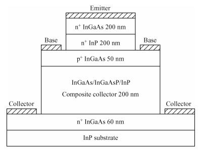
Fig. 1.
Layer structure of the InGaAs/InP DHBT.
SEMICONDUCTOR DEVICES
Wei Cheng, Yuan Wang, Yan Zhao, Haiyan Lu, Hanchao Gao and Naibin Yang
Corresponding author: Cheng Wei, Email:dspbuilder@yahoo.com.cn
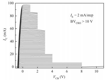
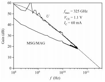
Abstract: A common-base four finger InGaAs/InP double heterostructure bipolar transistor (DHBT) has been designed and fabricated using triple mesa structure and planarization technology. All processes are on 3-inch wafers. The area of each emitter finger is 1×15 μm2. The maximum oscillation frequency (fmax) is 325 GHz and the breakdown voltage BVCBO is 10.6 V, which are to our knowledge both the highest fmax and BVCBO ever reported for InGaAs/InP DHBTs in China. The high speed InGaAs/InP DHBT with a high breakdown voltage is promising for submillimeter-wave and THz electronics.
Keywords: InP, DHBT, THz, high breakdown
| [1] |
Samoska S. Towards terahertz MMIC amplifiers: present status and trends. IEEE MTT-S International Microwave Symposium Digest, 2006: 333
|
| [2] |
Lai R, Mei X B, Deal W R, et al. Sub-50 nm InP HEMT device with fmax greater than 1 THz. IEEE International Electron Devices Meeting, 2007: 609
|
| [3] |
Urteaga M, Pierson R, Rowell P, et al. 130 nm InP DHBTs with ft > 0. 5 THz and fmax > 1. 1 THz. Device Research Conference, 2011: 281
|
| [4] |
Jin Z, Su Y, Cheng W, et al. Common-base multi-finger submicron InGaAs/InP double heterojunction bipolar transistor with fmax of 305 GHz. Solid-State Electron, 2008, 52:1825 doi: 10.1016/j.sse.2008.09.004
|
| [5] |
Tanaka S, Amamiya Y, Murakami S, et al. Common base HBTs for Ka band applications. International Topical Symposium on Millimeter Waves, 1997: 27
|
| [6] |
Cheng W, Jin Z, Yu J, et al. Design of InGaAsP composite collector for InP DHBT. Chinese Journal of Semiconductors, 2007, 28:943
|
| [7] |
Jin Z, Su Y, Cheng W, et al. High breakdown voltage submicron InGaAs/InP double heterojunction bipolar transistor with ft=170 GHz and fmax=253 GHz. Chin Phys Lett, 2008, 25:2686 doi: 10.1088/0256-307X/25/7/098
|
| [8] |
Zhou L, Jin Z, Su Y, et al. Ultra high speed InP/InGaAs SHBTs with ft and fmax of 185 GHz. Journal of Semiconductors, 2010, 31:094007 doi: 10.1088/1674-4926/31/9/094007
|
| [9] |
Cai D, Li X, Zhao Y, et al. Ultra high speed InP DHBTs with ft=140 GHz and fmax=200 GHz. Semiconductor Technology, 2011, 36:743
|
| [10] |
Dahlstrom M, Rodwell M. Current density limits in InP DHBTs:collector current spreading and effective electron velocity. IEEE International Conference on Indium Phosphide and Related Materials, 2004:761
|
| [11] |
Griffith Z. Ultra high speed InGaAs/InP DHBT devices and circuits. PhD Thesis, UC Santa Barbara, 2003
|


Article views: 3293 Times PDF downloads: 39 Times Cited by: 0 Times
Received: 25 August 2012 Revised: 22 October 2012 Online: Published: 01 May 2013
| Citation: |
Wei Cheng, Yuan Wang, Yan Zhao, Haiyan Lu, Hanchao Gao, Naibin Yang. A THz InGaAs/InP double heterojunction bipolar transistor with fmax=325 GHz and BVCBO=10.6 V[J]. Journal of Semiconductors, 2013, 34(5): 054006. doi: 10.1088/1674-4926/34/5/054006
****
W Cheng, Y Wang, Y Zhao, H Y Lu, H C Gao, N B Yang. A THz InGaAs/InP double heterojunction bipolar transistor with fmax=325 GHz and BVCBO=10.6 V[J]. J. Semicond., 2013, 34(5): 054006. doi: 10.1088/1674-4926/34/5/054006.

|
| [1] |
Samoska S. Towards terahertz MMIC amplifiers: present status and trends. IEEE MTT-S International Microwave Symposium Digest, 2006: 333
|
| [2] |
Lai R, Mei X B, Deal W R, et al. Sub-50 nm InP HEMT device with fmax greater than 1 THz. IEEE International Electron Devices Meeting, 2007: 609
|
| [3] |
Urteaga M, Pierson R, Rowell P, et al. 130 nm InP DHBTs with ft > 0. 5 THz and fmax > 1. 1 THz. Device Research Conference, 2011: 281
|
| [4] |
Jin Z, Su Y, Cheng W, et al. Common-base multi-finger submicron InGaAs/InP double heterojunction bipolar transistor with fmax of 305 GHz. Solid-State Electron, 2008, 52:1825 doi: 10.1016/j.sse.2008.09.004
|
| [5] |
Tanaka S, Amamiya Y, Murakami S, et al. Common base HBTs for Ka band applications. International Topical Symposium on Millimeter Waves, 1997: 27
|
| [6] |
Cheng W, Jin Z, Yu J, et al. Design of InGaAsP composite collector for InP DHBT. Chinese Journal of Semiconductors, 2007, 28:943
|
| [7] |
Jin Z, Su Y, Cheng W, et al. High breakdown voltage submicron InGaAs/InP double heterojunction bipolar transistor with ft=170 GHz and fmax=253 GHz. Chin Phys Lett, 2008, 25:2686 doi: 10.1088/0256-307X/25/7/098
|
| [8] |
Zhou L, Jin Z, Su Y, et al. Ultra high speed InP/InGaAs SHBTs with ft and fmax of 185 GHz. Journal of Semiconductors, 2010, 31:094007 doi: 10.1088/1674-4926/31/9/094007
|
| [9] |
Cai D, Li X, Zhao Y, et al. Ultra high speed InP DHBTs with ft=140 GHz and fmax=200 GHz. Semiconductor Technology, 2011, 36:743
|
| [10] |
Dahlstrom M, Rodwell M. Current density limits in InP DHBTs:collector current spreading and effective electron velocity. IEEE International Conference on Indium Phosphide and Related Materials, 2004:761
|
| [11] |
Griffith Z. Ultra high speed InGaAs/InP DHBT devices and circuits. PhD Thesis, UC Santa Barbara, 2003
|

 WeChat ID
Journal of Semiconductors © 2017 All Rights Reserved 京ICP备05085259号-2

 DownLoad:

