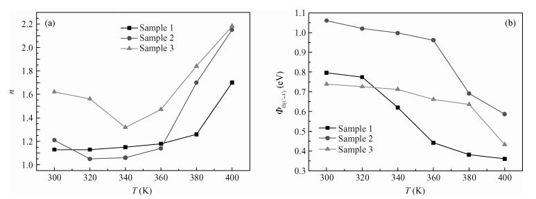
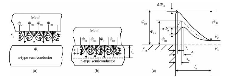
| [1] |
|
| [2] |
Mott N F. Note on the contact between a metal and an insulator or semiconductor. Proc Cambridge Philos Soc, 1938, 34:568 doi: 10.1017/S0305004100020570 |
| [3] |
Bardeen J. Surface states and rectification at a metal semiconductor contact. Phys Rev, 1947, 71:717 doi: 10.1103/PhysRev.71.717 |
| [4] |
Tung T. Electron transport of inhomogeneous Schottky barriers. Appl Phys Lett, 1991, 58(24):2821 doi: 10.1063/1.104747 |
| [5] |
Sullivan J P, Tung R T, Pinto M R, et al. Electron transport of inhomogeneous Schottky barriers:a numerical study. J Appl Phys, 1991, 70:7403 doi: 10.1063/1.349737 |
| [6] |
|
| [7] |
Tung R T, Brilson L J. Contacts to semiconductors. New Jersey:Noyes Publishers, 1993
|
| [8] |
Werner J H, Guttler H H. Barrier inhomogeneities at Schottky contacts. J Appl Phys, 1991, 69:1522 doi: 10.1063/1.347243 |
| [9] |
|
| [10] |
Monch W. Barrier heights of real Schottky contacts explained by metal-induced gap states and lateral in homogeneities. J Vac Sci Technol B, 1999, 17:1867 doi: 10.1116/1.590839 |
| [11] |
|
| [12] |
Sato T, Kasai S, Okada H, et al. Electrical properties of nanometer-sized Schottky contacts on n-GaAs and n-InP formed by in situ electrochemical process. Jpn J Appl Phys, 2000, 39:4609 doi: 10.1143/JJAP.39.4609 |
| [13] |
Ayyildiz E, Cetin H, Horvath Z J. Temperature dependent electrical characteristics of Sn/p-Si Schottky diodes. Appl Surf Sci, 2005, 252:1153 doi: 10.1016/j.apsusc.2005.02.044 |
| [14] |
Osvald J, Horvath Z J. Theoretical study of the temperature dependence of electrical characteristics of Schottky diodes with an inverse near-surface layer. Appl Surf Sci, 2004, 234:349 doi: 10.1016/j.apsusc.2004.05.046 |
| [15] |
Nuhoglu C, Ozerden E, Turut A. The dependence of I-V and C-V characteristics on temperature in the H-terminated Pb/p-Si (100) Schottky barrier diodes. Appl Surf Sci, 2005, 250:203 doi: 10.1016/j.apsusc.2004.12.047 |
| [16] |
Farag A A M, Ashery A, Ahmed E M A, et al. Effect of temperature, illumination and frequency on the electrical characteristics of Cu/p-Si Schottky diode prepared by liquid phase epitaxy. Journal of Alloys and Compounds, 2010, 495:116 doi: 10.1016/j.jallcom.2010.01.098 |
| [17] |
Karatas S, Altındal S, Turut A, et al. Electrical transport characteristics of Sn/p-Si Schottky contacts revealed from I- V- T and C- V- T measurements. Physica B, 2007, 392:43 doi: 10.1016/j.physb.2006.10.039 |
| [18] |
Shah M, Sayyad M H, Karimov K S, et al. Investigation of the electrical properties of a surface-type Al/NiPc/Ag Schottky diode using I-V and C-V characteristics. Physica B, 2010, 405:1188 doi: 10.1016/j.physb.2009.11.034 |
| [19] |
Reddy M B, Kumar A A, Janardhanam V, et al. Current-voltage-temperature ( I-V-T) characteristics of Pd/Au Schottky contacts on n-InP (111). Current Appl Phys, 2009, 9:972 doi: 10.1016/j.cap.2008.10.001 |
| [20] |
Yüksel Ö F. Temperature dependence of current-voltage characteristics of Al/p-Si (100) Schottky barrier diodes. Physica B, 2009, 404:1993 doi: 10.1016/j.physb.2009.03.026 |
| [21] |
Huang W C, Chen C C. Electrical characteristics and in homogeneous barrier analysis of Al/NPB/p-Si Schottky diodes. Microelectron Eng, 2011, 88:287 doi: 10.1016/j.mee.2010.11.023 |
| [22] |
Tunc T, Altindal S, Uslu I, et al. Temperature dependent current-voltage ( I-V) characteristics of Au/n-Si (111) Schottky barrier diodes with PVA (Ni, Zn-doped) interfacial layer. Materials Science in Semiconductor Processing, 2011, 14:139 doi: 10.1016/j.mssp.2011.01.018 |
| [23] |
Aydın M E, Gullu O, Yıldırım N. Temperature dependence of current-voltage characteristics of Sn/p-Si Schottky contacts. Physica B, 2008, 403:131 doi: 10.1016/j.physb.2007.08.089 |
| [24] |
Nuhoglu C, Gulen Y. The dependence of I-V and C-V characteristics on temperature in the H-terminated Pb/p-Si(100) Schottky barrier diodes. Vacuum, 2010, 84:812 doi: 10.1016/j.vacuum.2009.10.049 |
| [25] |
Osvald J. Temperature dependence of barrier height parameters of inhomogeneous Schottky diodes. Microelectron Eng, 2009, 86(1):117 doi: 10.1016/j.mee.2008.10.006 |
| [26] |
Maeda K. Nonideality of Au/Si and Au/GaAs Schottky barriers due to process-induced defects. Appl Surf Sci, 2006, 252:5659 doi: 10.1016/j.apsusc.2005.07.074 |
| [27] |
Naik S S, Reddy V R. Electrical transport characteristics and deep level transient spectroscopy of Ni/V/n-InP Schottky barrier diodes. J Nano-Electron Phys, 2011, 3(1):1048 http://www.oalib.com/paper/2847224 |
| [28] |
|
| [29] |
Al-Heniti S, Badran R I, Umar A, et al. Temperature dependant structural and electrical properties of ZnO nanowire networks. Journal of Nanoscience and Nanotechnology, 2011, 11:1 doi: 10.1166/jnn.2011.3839 |
| [30] |
Naik S S, Reddy V R. Temperature dependency and current transport mechanisms of Pd/V/n-type InP Schottky rectifiers. Adv Mat Lett, 2012, 3(3):188 doi: 10.5185/amlett |
| [31] |
Khannaa S, Neeleshwara S, Noorb A. Current-voltage-temperature ( I-V-T) characteristics of CR/4H-SIC Schottky diodes. Journal of Electron Devices, 2011, 9:382 http://www.jeldev.org/9Shaweta.pdf |
| [32] |
Mamedov R K. Contacts metal-semiconductor with electrical spots field. Baku State University Press, 2003:1 doi: 10.1134/S1063782611080227 |


 DownLoad: