


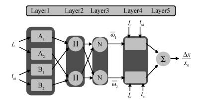
Fig. 1.
Illustrative representation of ANFIS with two input parameters and two MFs.
SEMICONDUCTOR DEVICES
T. Bentrcia1, F. Djeffal2, 3, and E. Chebaaki2
Corresponding author: F. Djeffal, Email:faycal.djeffal@univ-batna.dz, faycaldzdz@hotmail.com
Abstract: A fuzzy framework based on an adaptive network fuzzy inference system (ANFIS) is proposed to evaluate the relative degradation of the basic subthreshold parameters due to hot-carrier effects for nanoscale thin-film double-gate (DG) MOSFETs. The effect of the channel length and thickness on the resulting degradation is addressed, and 2-D numerical simulations are used for the elaboration of the training database. Several membership function shapes are developed, and the best one in terms of accuracy is selected. The predicted results agree well with the 2-D numerical simulations and can be efficiently used to investigate the impact of the interface fixed charges and quantum confinement on nanoscale DG MOSFET subthreshold behavior. Therefore, the proposed ANFIS-based approach offers a simple and accurate technique to study nanoscale devices, including the hot-carrier and quantum effects.
Keywords: hot-carrier degradation, ANFIS, fuzzy computation, subthreshold, quantum effects, thin film
| [1] |
Kaur H, Kabra S, Haldar S, et al. An analytical drain current model for graded channel cylindrical/surrounding gate MOSFET. Microelectron J, 2007, 38:352 doi: 10.1016/j.mejo.2007.01.003
|
| [2] |
Amat E, Rodrìguez R, Nafrìa M, et al. Channel hot-carrier degradation under AC stress in short channel nMOS devices with high-k gate stacks. Microelectron Eng, 2009, 86:1908 doi: 10.1016/j.mee.2009.03.031
|
| [3] |
Ghosh P, Haldar S, Gupta R S, et al. An analytical drain current model for dual material engineered cylindrical/surrounded gate MOSFET. Microelectron J, 2012, 43:17 doi: 10.1016/j.mejo.2011.10.001
|
| [4] |
International Technology Roadmap for Semiconductors (ITRS), Published online at http://public.itrs.net, 2009
|
| [5] |
Difrenza R, Linares P, Ghibaudo G. The impact of short channel and quantum effects on the MOS transistor mismatch. Solid-State Electron, 2003, 47:1161 doi: 10.1016/S0038-1101(03)00033-9
|
| [6] |
Bentrcia T, Djeffal F. Compact modeling of multi-gate MOSFET including hot-carrier effects. CMOS Technology:Electrical Engineering Developments Series, Vol. 1. Chap. 4. New York:Nova Publishers, 2011
|
| [7] |
Pagey M P. Hot-carrier reliability simulation in aggressively scaled MOS transistors. PhD Dissertation, Electrical Engineering Department, Vanderbilt University, Nashville, Tennessee, USA, 2003 http://etd.library.vanderbilt.edu/available/etd-12032003-100902/unrestricted/Thesis.pdf
|
| [8] |
Prégaldiny F, Lallement C, Mathiot D. Accounting for quantum mechanical effects from accumulation to inversion, in a fully analytical surface-potential-based MOSFET model. Solid-State Electron, 2004, 48:781 doi: 10.1016/j.sse.2003.12.010
|
| [9] |
Ghoggali Z, Djeffal F, Lakhdar N. Analytical analysis of nanoscale double-gate MOSFETs including the hot-carrier degradation effects. Int J Electron, 2010, 97:119 doi: 10.1080/00207210902894746
|
| [10] |
Bendib T, Djeffal F. Electrical performance optimization of nanoscale double-gate MOSFETs using multi-objective genetic algorithms. IEEE Trans Electron Devices, 2011, 58:3743 doi: 10.1109/TED.2011.2163820
|
| [11] |
Bentrcia T, Djeffal F, Benhaya A. Continuous analytic Ⅳ model for GS DG MOSFETs including hot-carrier degradation effects. Journal of Semiconductors, 2012, 33:014001 doi: 10.1088/1674-4926/33/1/014001
|
| [12] |
Djeffal F, Bentrcia T, Abdi M A, et al. Drain current model for undoped gate stack double gate (GSDG) MOSFETs including the hot-carrier degradation effects. Microelectron Reliab, 2011, 51:550 doi: 10.1016/j.microrel.2010.10.002
|
| [13] |
Djeffal F, Bentrcia T, Bendib T. An analytical drain current model for undoped GSDG MOSFETs including interfacial hot-carrier effects. Phys Status Solidi C, 2011, 8:907 doi: 10.1002/pssc.201000158
|
| [14] |
Tyaginov S E, Starkov I A, Triebl O, et al. Interface traps density-of-states as a vital component for hot-carrier degradation modeling. Microelectron Reliab, 2010, 50:1267 doi: 10.1016/j.microrel.2010.07.030
|
| [15] |
Eisberg R, Renick R. Notes on modern physics. John Wiley and Sons, NY, 1969
|
| [16] |
Djeffal F, Bendib T, Abdi M A. A two-dimensional semi-analytical analysis of the subthreshold-swing behavior including free carriers and interfacial traps effects for nanoscale double-gate MOSFETs. Microelectron J, 2011, 42:1391 doi: 10.1016/j.mejo.2011.09.008
|
| [17] |
Ho C S, Huang K Y, Tang M, et al. An analytical threshold voltage model of NMOSFETs with hot-carrier induced interface charge effect. Microelectron Reliab, 2005, 45:1144 doi: 10.1016/j.microrel.2004.10.007
|
| [18] |
Mahapatra S, Parikh C D, Rao V R, et al. A Comprehensive study of hot-carrier induced interface and oxide trap distributions in MOSFET's using a novel charge pumping technique. IEEE Trans Electron Devices, 2000, 47:171 doi: 10.1109/16.817583
|
| [19] |
Singh A K. An analytical study of hot-carrier degradation effects in sub-micron MOS devices. The European Physical Journal Applied Physics, 2008, 42(2):87 doi: 10.1051/epjap:2008047
|
| [20] |
Naseh S, Deen M J, Chen C. Hot-carrier reliability of submicron nMOSFETs and integrated nMOS low noise amplifiers. Microelectron Reliab, 2006, 46:201 doi: 10.1016/j.microrel.2005.04.009
|
| [21] |
Zadeh L A. Outline of a new approach to the analysis of complex systems and decision processes. IEEE Trans Syst, Man, Cybernetics, 1973, 3:28 http://www.oalib.com/references/13118707
|
| [22] |
Jang J. ANFIS:adaptive-network-based fuzzy inference system. IEEE Trans Syst Man Cybernytics, 1993, 23:665 doi: 10.1109/21.256541
|
| [23] |
Lo S P. An adaptive-network based fuzzy inference system for prediction of work piece surface roughness in end milling. Journal of Materials Processing Technology, 2003, 142: 665
|
| [24] |
Ying L C, Pan M C. Using adaptive network based fuzzy inference system to forecast regional electricity loads. Energy Conversion and Management, 2008, 49:205 doi: 10.1016/j.enconman.2007.06.015
|
| [25] |
Akdemïr B, Günes S, Oran B, et al. Prediction of cardiac end-systolic and end-diastolic diameters in m-mode values using adaptive neural fuzzy inference system. Expert Systems with Applications, 2010, 37:5720 doi: 10.1016/j.eswa.2010.02.038
|
| [26] |
Singh M. Adaptive network-based fuzzy inference systems for sensorless control of PMSG based wind turbine with power quality improvement features. PhD Dissertation, University of Quebec, MONTREAL, 16 JULY 2010
|
| [27] |
Lawson C L, Hanson R J. Solving least squares problems. Englewood Cliffs, NJ: Prentice-Hall, 1974
|
| [28] |
Nariman-Zadeh N, Darvizeh A, Dadfarmai M H. Design of ANFIS networks using hybrid genetic and SVD methods for the modelling of explosive cutting process. Journal of Materials Processing Technology, 2004, 155:1415 doi: 10.1007/s12239-009-0020-6
|
| [29] |
Jiang H M, Kwong C K, Ip W H, et al. Modeling customer satisfaction for new product development using a PSO-based ANFIS approach. Applied Soft Computing, 2012, 12:726 doi: 10.1016/j.asoc.2011.10.020
|
| [30] |
Atlas User's Manual: Device Simulation Software, 2008
|
| [31] |
Djeffal F, Ghoggali Z, Dibi Z, et al. Analytical analysis of nanoscale multiple gate MOSFETs including effects of hot-carrier induced interface charges. Microelectron Reliab, 2009, 49:377 doi: 10.1016/j.microrel.2008.12.011
|
| [32] |
Bentrcia T, Djeffal F, Abdi M A, et al. An accurate two dimensional threshold voltage model for nanoscale GCGS DGMOSFET including traps effects. 3rd IEEE International Conference on Signals, Circuits and Systems, Djerba, Tunisia, 2009 doi: 10.1007/978-94-017-8832-8_25
|
| [33] |
Bentrcia T, Djeffal F, Arar D. An analytical two dimensional subthreshold current model for nanoscale GCGS DG MOSFET including interfacial traps effects. Rev Sci Technol, 2010, 1:103 doi: 10.1007%2Fs10825-010-0329-4.pdf
|
| [34] |
Djeffal F, Meguellati M, Benhaya A. A two-dimensional analytical analysis of subthreshold behavior to study the scaling capability of nanoscale graded channel gate stack DG MOSFETs. Physica E:Low-Dimensional Systems and Nanostructures, 2009, 41:1872 doi: 10.1016/j.physe.2009.08.002
|
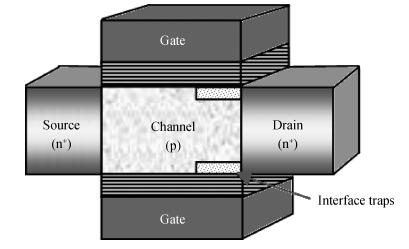
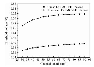
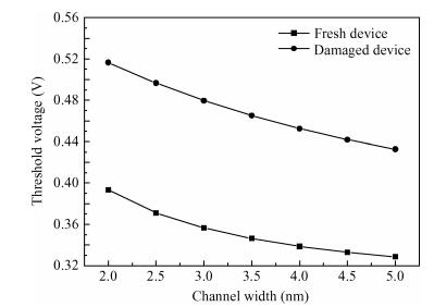
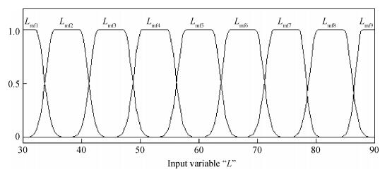
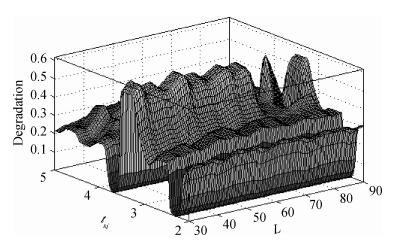
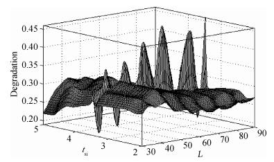
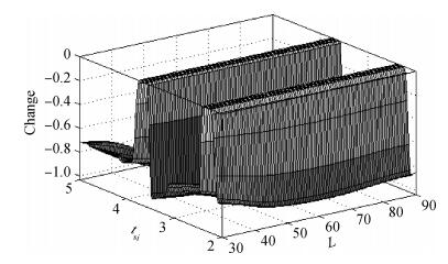
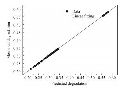
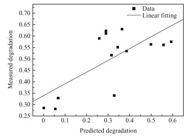
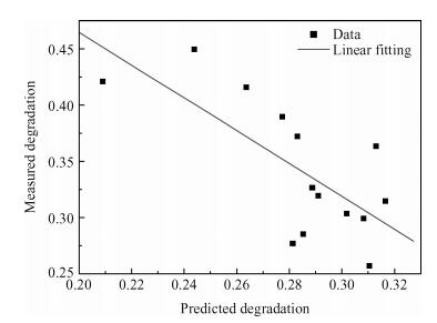
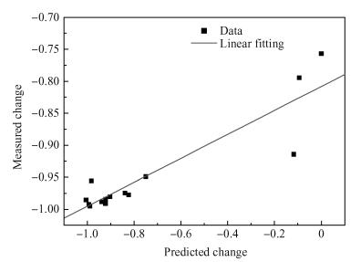
Table 1. Device design and simulation parameters.

|
Table 2. Summary of the main obtained results.

|
| [1] |
Kaur H, Kabra S, Haldar S, et al. An analytical drain current model for graded channel cylindrical/surrounding gate MOSFET. Microelectron J, 2007, 38:352 doi: 10.1016/j.mejo.2007.01.003
|
| [2] |
Amat E, Rodrìguez R, Nafrìa M, et al. Channel hot-carrier degradation under AC stress in short channel nMOS devices with high-k gate stacks. Microelectron Eng, 2009, 86:1908 doi: 10.1016/j.mee.2009.03.031
|
| [3] |
Ghosh P, Haldar S, Gupta R S, et al. An analytical drain current model for dual material engineered cylindrical/surrounded gate MOSFET. Microelectron J, 2012, 43:17 doi: 10.1016/j.mejo.2011.10.001
|
| [4] |
International Technology Roadmap for Semiconductors (ITRS), Published online at http://public.itrs.net, 2009
|
| [5] |
Difrenza R, Linares P, Ghibaudo G. The impact of short channel and quantum effects on the MOS transistor mismatch. Solid-State Electron, 2003, 47:1161 doi: 10.1016/S0038-1101(03)00033-9
|
| [6] |
Bentrcia T, Djeffal F. Compact modeling of multi-gate MOSFET including hot-carrier effects. CMOS Technology:Electrical Engineering Developments Series, Vol. 1. Chap. 4. New York:Nova Publishers, 2011
|
| [7] |
Pagey M P. Hot-carrier reliability simulation in aggressively scaled MOS transistors. PhD Dissertation, Electrical Engineering Department, Vanderbilt University, Nashville, Tennessee, USA, 2003 http://etd.library.vanderbilt.edu/available/etd-12032003-100902/unrestricted/Thesis.pdf
|
| [8] |
Prégaldiny F, Lallement C, Mathiot D. Accounting for quantum mechanical effects from accumulation to inversion, in a fully analytical surface-potential-based MOSFET model. Solid-State Electron, 2004, 48:781 doi: 10.1016/j.sse.2003.12.010
|
| [9] |
Ghoggali Z, Djeffal F, Lakhdar N. Analytical analysis of nanoscale double-gate MOSFETs including the hot-carrier degradation effects. Int J Electron, 2010, 97:119 doi: 10.1080/00207210902894746
|
| [10] |
Bendib T, Djeffal F. Electrical performance optimization of nanoscale double-gate MOSFETs using multi-objective genetic algorithms. IEEE Trans Electron Devices, 2011, 58:3743 doi: 10.1109/TED.2011.2163820
|
| [11] |
Bentrcia T, Djeffal F, Benhaya A. Continuous analytic Ⅳ model for GS DG MOSFETs including hot-carrier degradation effects. Journal of Semiconductors, 2012, 33:014001 doi: 10.1088/1674-4926/33/1/014001
|
| [12] |
Djeffal F, Bentrcia T, Abdi M A, et al. Drain current model for undoped gate stack double gate (GSDG) MOSFETs including the hot-carrier degradation effects. Microelectron Reliab, 2011, 51:550 doi: 10.1016/j.microrel.2010.10.002
|
| [13] |
Djeffal F, Bentrcia T, Bendib T. An analytical drain current model for undoped GSDG MOSFETs including interfacial hot-carrier effects. Phys Status Solidi C, 2011, 8:907 doi: 10.1002/pssc.201000158
|
| [14] |
Tyaginov S E, Starkov I A, Triebl O, et al. Interface traps density-of-states as a vital component for hot-carrier degradation modeling. Microelectron Reliab, 2010, 50:1267 doi: 10.1016/j.microrel.2010.07.030
|
| [15] |
Eisberg R, Renick R. Notes on modern physics. John Wiley and Sons, NY, 1969
|
| [16] |
Djeffal F, Bendib T, Abdi M A. A two-dimensional semi-analytical analysis of the subthreshold-swing behavior including free carriers and interfacial traps effects for nanoscale double-gate MOSFETs. Microelectron J, 2011, 42:1391 doi: 10.1016/j.mejo.2011.09.008
|
| [17] |
Ho C S, Huang K Y, Tang M, et al. An analytical threshold voltage model of NMOSFETs with hot-carrier induced interface charge effect. Microelectron Reliab, 2005, 45:1144 doi: 10.1016/j.microrel.2004.10.007
|
| [18] |
Mahapatra S, Parikh C D, Rao V R, et al. A Comprehensive study of hot-carrier induced interface and oxide trap distributions in MOSFET's using a novel charge pumping technique. IEEE Trans Electron Devices, 2000, 47:171 doi: 10.1109/16.817583
|
| [19] |
Singh A K. An analytical study of hot-carrier degradation effects in sub-micron MOS devices. The European Physical Journal Applied Physics, 2008, 42(2):87 doi: 10.1051/epjap:2008047
|
| [20] |
Naseh S, Deen M J, Chen C. Hot-carrier reliability of submicron nMOSFETs and integrated nMOS low noise amplifiers. Microelectron Reliab, 2006, 46:201 doi: 10.1016/j.microrel.2005.04.009
|
| [21] |
Zadeh L A. Outline of a new approach to the analysis of complex systems and decision processes. IEEE Trans Syst, Man, Cybernetics, 1973, 3:28 http://www.oalib.com/references/13118707
|
| [22] |
Jang J. ANFIS:adaptive-network-based fuzzy inference system. IEEE Trans Syst Man Cybernytics, 1993, 23:665 doi: 10.1109/21.256541
|
| [23] |
Lo S P. An adaptive-network based fuzzy inference system for prediction of work piece surface roughness in end milling. Journal of Materials Processing Technology, 2003, 142: 665
|
| [24] |
Ying L C, Pan M C. Using adaptive network based fuzzy inference system to forecast regional electricity loads. Energy Conversion and Management, 2008, 49:205 doi: 10.1016/j.enconman.2007.06.015
|
| [25] |
Akdemïr B, Günes S, Oran B, et al. Prediction of cardiac end-systolic and end-diastolic diameters in m-mode values using adaptive neural fuzzy inference system. Expert Systems with Applications, 2010, 37:5720 doi: 10.1016/j.eswa.2010.02.038
|
| [26] |
Singh M. Adaptive network-based fuzzy inference systems for sensorless control of PMSG based wind turbine with power quality improvement features. PhD Dissertation, University of Quebec, MONTREAL, 16 JULY 2010
|
| [27] |
Lawson C L, Hanson R J. Solving least squares problems. Englewood Cliffs, NJ: Prentice-Hall, 1974
|
| [28] |
Nariman-Zadeh N, Darvizeh A, Dadfarmai M H. Design of ANFIS networks using hybrid genetic and SVD methods for the modelling of explosive cutting process. Journal of Materials Processing Technology, 2004, 155:1415 doi: 10.1007/s12239-009-0020-6
|
| [29] |
Jiang H M, Kwong C K, Ip W H, et al. Modeling customer satisfaction for new product development using a PSO-based ANFIS approach. Applied Soft Computing, 2012, 12:726 doi: 10.1016/j.asoc.2011.10.020
|
| [30] |
Atlas User's Manual: Device Simulation Software, 2008
|
| [31] |
Djeffal F, Ghoggali Z, Dibi Z, et al. Analytical analysis of nanoscale multiple gate MOSFETs including effects of hot-carrier induced interface charges. Microelectron Reliab, 2009, 49:377 doi: 10.1016/j.microrel.2008.12.011
|
| [32] |
Bentrcia T, Djeffal F, Abdi M A, et al. An accurate two dimensional threshold voltage model for nanoscale GCGS DGMOSFET including traps effects. 3rd IEEE International Conference on Signals, Circuits and Systems, Djerba, Tunisia, 2009 doi: 10.1007/978-94-017-8832-8_25
|
| [33] |
Bentrcia T, Djeffal F, Arar D. An analytical two dimensional subthreshold current model for nanoscale GCGS DG MOSFET including interfacial traps effects. Rev Sci Technol, 2010, 1:103 doi: 10.1007%2Fs10825-010-0329-4.pdf
|
| [34] |
Djeffal F, Meguellati M, Benhaya A. A two-dimensional analytical analysis of subthreshold behavior to study the scaling capability of nanoscale graded channel gate stack DG MOSFETs. Physica E:Low-Dimensional Systems and Nanostructures, 2009, 41:1872 doi: 10.1016/j.physe.2009.08.002
|


Article views: 3186 Times PDF downloads: 18 Times Cited by: 0 Times
Received: 11 January 2013 Revised: 10 February 2013 Online: Published: 01 August 2013
| Citation: |
T. Bentrcia, F. Djeffal, E. Chebaaki. ANFIS-based approach to studying subthreshold behavior including the traps effect for nanoscale thin-film DG MOSFETs[J]. Journal of Semiconductors, 2013, 34(8): 084001. doi: 10.1088/1674-4926/34/8/084001
****
T. Bentrcia, F. Djeffal, E. Chebaaki. ANFIS-based approach to studying subthreshold behavior including the traps effect for nanoscale thin-film DG MOSFETs[J]. J. Semicond., 2013, 34(8): 084001. doi: 10.1088/1674-4926/34/8/084001.

|
| [1] |
Kaur H, Kabra S, Haldar S, et al. An analytical drain current model for graded channel cylindrical/surrounding gate MOSFET. Microelectron J, 2007, 38:352 doi: 10.1016/j.mejo.2007.01.003
|
| [2] |
Amat E, Rodrìguez R, Nafrìa M, et al. Channel hot-carrier degradation under AC stress in short channel nMOS devices with high-k gate stacks. Microelectron Eng, 2009, 86:1908 doi: 10.1016/j.mee.2009.03.031
|
| [3] |
Ghosh P, Haldar S, Gupta R S, et al. An analytical drain current model for dual material engineered cylindrical/surrounded gate MOSFET. Microelectron J, 2012, 43:17 doi: 10.1016/j.mejo.2011.10.001
|
| [4] |
International Technology Roadmap for Semiconductors (ITRS), Published online at http://public.itrs.net, 2009
|
| [5] |
Difrenza R, Linares P, Ghibaudo G. The impact of short channel and quantum effects on the MOS transistor mismatch. Solid-State Electron, 2003, 47:1161 doi: 10.1016/S0038-1101(03)00033-9
|
| [6] |
Bentrcia T, Djeffal F. Compact modeling of multi-gate MOSFET including hot-carrier effects. CMOS Technology:Electrical Engineering Developments Series, Vol. 1. Chap. 4. New York:Nova Publishers, 2011
|
| [7] |
Pagey M P. Hot-carrier reliability simulation in aggressively scaled MOS transistors. PhD Dissertation, Electrical Engineering Department, Vanderbilt University, Nashville, Tennessee, USA, 2003 http://etd.library.vanderbilt.edu/available/etd-12032003-100902/unrestricted/Thesis.pdf
|
| [8] |
Prégaldiny F, Lallement C, Mathiot D. Accounting for quantum mechanical effects from accumulation to inversion, in a fully analytical surface-potential-based MOSFET model. Solid-State Electron, 2004, 48:781 doi: 10.1016/j.sse.2003.12.010
|
| [9] |
Ghoggali Z, Djeffal F, Lakhdar N. Analytical analysis of nanoscale double-gate MOSFETs including the hot-carrier degradation effects. Int J Electron, 2010, 97:119 doi: 10.1080/00207210902894746
|
| [10] |
Bendib T, Djeffal F. Electrical performance optimization of nanoscale double-gate MOSFETs using multi-objective genetic algorithms. IEEE Trans Electron Devices, 2011, 58:3743 doi: 10.1109/TED.2011.2163820
|
| [11] |
Bentrcia T, Djeffal F, Benhaya A. Continuous analytic Ⅳ model for GS DG MOSFETs including hot-carrier degradation effects. Journal of Semiconductors, 2012, 33:014001 doi: 10.1088/1674-4926/33/1/014001
|
| [12] |
Djeffal F, Bentrcia T, Abdi M A, et al. Drain current model for undoped gate stack double gate (GSDG) MOSFETs including the hot-carrier degradation effects. Microelectron Reliab, 2011, 51:550 doi: 10.1016/j.microrel.2010.10.002
|
| [13] |
Djeffal F, Bentrcia T, Bendib T. An analytical drain current model for undoped GSDG MOSFETs including interfacial hot-carrier effects. Phys Status Solidi C, 2011, 8:907 doi: 10.1002/pssc.201000158
|
| [14] |
Tyaginov S E, Starkov I A, Triebl O, et al. Interface traps density-of-states as a vital component for hot-carrier degradation modeling. Microelectron Reliab, 2010, 50:1267 doi: 10.1016/j.microrel.2010.07.030
|
| [15] |
Eisberg R, Renick R. Notes on modern physics. John Wiley and Sons, NY, 1969
|
| [16] |
Djeffal F, Bendib T, Abdi M A. A two-dimensional semi-analytical analysis of the subthreshold-swing behavior including free carriers and interfacial traps effects for nanoscale double-gate MOSFETs. Microelectron J, 2011, 42:1391 doi: 10.1016/j.mejo.2011.09.008
|
| [17] |
Ho C S, Huang K Y, Tang M, et al. An analytical threshold voltage model of NMOSFETs with hot-carrier induced interface charge effect. Microelectron Reliab, 2005, 45:1144 doi: 10.1016/j.microrel.2004.10.007
|
| [18] |
Mahapatra S, Parikh C D, Rao V R, et al. A Comprehensive study of hot-carrier induced interface and oxide trap distributions in MOSFET's using a novel charge pumping technique. IEEE Trans Electron Devices, 2000, 47:171 doi: 10.1109/16.817583
|
| [19] |
Singh A K. An analytical study of hot-carrier degradation effects in sub-micron MOS devices. The European Physical Journal Applied Physics, 2008, 42(2):87 doi: 10.1051/epjap:2008047
|
| [20] |
Naseh S, Deen M J, Chen C. Hot-carrier reliability of submicron nMOSFETs and integrated nMOS low noise amplifiers. Microelectron Reliab, 2006, 46:201 doi: 10.1016/j.microrel.2005.04.009
|
| [21] |
Zadeh L A. Outline of a new approach to the analysis of complex systems and decision processes. IEEE Trans Syst, Man, Cybernetics, 1973, 3:28 http://www.oalib.com/references/13118707
|
| [22] |
Jang J. ANFIS:adaptive-network-based fuzzy inference system. IEEE Trans Syst Man Cybernytics, 1993, 23:665 doi: 10.1109/21.256541
|
| [23] |
Lo S P. An adaptive-network based fuzzy inference system for prediction of work piece surface roughness in end milling. Journal of Materials Processing Technology, 2003, 142: 665
|
| [24] |
Ying L C, Pan M C. Using adaptive network based fuzzy inference system to forecast regional electricity loads. Energy Conversion and Management, 2008, 49:205 doi: 10.1016/j.enconman.2007.06.015
|
| [25] |
Akdemïr B, Günes S, Oran B, et al. Prediction of cardiac end-systolic and end-diastolic diameters in m-mode values using adaptive neural fuzzy inference system. Expert Systems with Applications, 2010, 37:5720 doi: 10.1016/j.eswa.2010.02.038
|
| [26] |
Singh M. Adaptive network-based fuzzy inference systems for sensorless control of PMSG based wind turbine with power quality improvement features. PhD Dissertation, University of Quebec, MONTREAL, 16 JULY 2010
|
| [27] |
Lawson C L, Hanson R J. Solving least squares problems. Englewood Cliffs, NJ: Prentice-Hall, 1974
|
| [28] |
Nariman-Zadeh N, Darvizeh A, Dadfarmai M H. Design of ANFIS networks using hybrid genetic and SVD methods for the modelling of explosive cutting process. Journal of Materials Processing Technology, 2004, 155:1415 doi: 10.1007/s12239-009-0020-6
|
| [29] |
Jiang H M, Kwong C K, Ip W H, et al. Modeling customer satisfaction for new product development using a PSO-based ANFIS approach. Applied Soft Computing, 2012, 12:726 doi: 10.1016/j.asoc.2011.10.020
|
| [30] |
Atlas User's Manual: Device Simulation Software, 2008
|
| [31] |
Djeffal F, Ghoggali Z, Dibi Z, et al. Analytical analysis of nanoscale multiple gate MOSFETs including effects of hot-carrier induced interface charges. Microelectron Reliab, 2009, 49:377 doi: 10.1016/j.microrel.2008.12.011
|
| [32] |
Bentrcia T, Djeffal F, Abdi M A, et al. An accurate two dimensional threshold voltage model for nanoscale GCGS DGMOSFET including traps effects. 3rd IEEE International Conference on Signals, Circuits and Systems, Djerba, Tunisia, 2009 doi: 10.1007/978-94-017-8832-8_25
|
| [33] |
Bentrcia T, Djeffal F, Arar D. An analytical two dimensional subthreshold current model for nanoscale GCGS DG MOSFET including interfacial traps effects. Rev Sci Technol, 2010, 1:103 doi: 10.1007%2Fs10825-010-0329-4.pdf
|
| [34] |
Djeffal F, Meguellati M, Benhaya A. A two-dimensional analytical analysis of subthreshold behavior to study the scaling capability of nanoscale graded channel gate stack DG MOSFETs. Physica E:Low-Dimensional Systems and Nanostructures, 2009, 41:1872 doi: 10.1016/j.physe.2009.08.002
|

 WeChat ID
Journal of Semiconductors © 2017 All Rights Reserved 京ICP备05085259号-2

 DownLoad:

