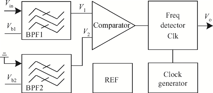
Fig. 1.
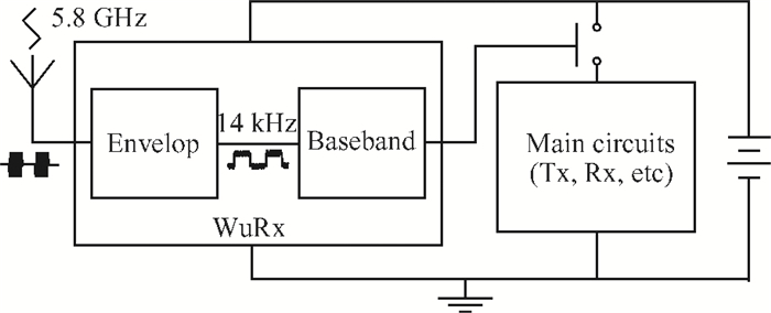
Block diagram of a typical OBU.
SEMICONDUCTOR INTEGRATED CIRCUITS
Wenrui Zhu1, 2, Haigang Yang1, , Tongqiang Gao1, Fei Liu1, Xiaoyan Cheng1, 2 and Dandan Zhang1, 2
Corresponding author: Yang Haigang, Email:yanghg@mail.ie.ac.cn
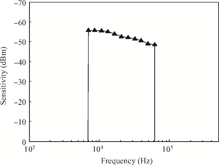
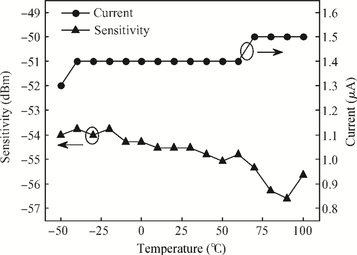
Abstract: This paper proposes a baseband circuit for wake-up receivers with double-mode detection and enhanced sensitivity robustness for use in the electronic toll collection system. A double-mode detection method, including amplitude detection and frequency detection, is proposed to reject interference and reduce false wake-ups. An improved closed-loop band-pass filter and a DC offset cancellation technique are also newly introduced to enhance the sensitivity robustness. The circuit is fabricated in TSMC 0.18 μm 3.3 V CMOS technology with an area of 0.12 mm2. Measurement results show that the sensitivity is -54.5 dBm with only a ±0.95 dBm variation from the 1.8 to 3.3 V power supply, and that the temperature variation of the sensitivity is ±1.4 dBm from -50 to 100℃. The current consumption is 1.4 to 1.7 μA under a 1.8 to 3.3 V power supply.
Keywords: wake-up receiver, double-mode detection, DC offset cancellation
| [1] |
Yoon D Y, Jeong C J, Cartwright J, et al. A new approach to low-power and low-latency wake-up receiver system for wireless sensor nodes. IEEE J Solid-State Circuits, 2012, 47:2405 doi: 10.1109/JSSC.2012.2209778
|
| [2] |
Marinkovic S, Popovici E. Nano-power wake-up radio circuit for wireless body area networks. IEEE Radio and Wireless Symposium (RWS), 2011:398 http://ieeexplore.ieee.org/document/5725447/?tp=&arnumber=5725447&contentType=Conference%20Publications&sortType%3Ddesc_p_Publication_Year%26searchField%3DSearch_All%26queryText%3DNano-power%20Circuit
|
| [3] |
Milosiu H, Meier F, Preiss H, et al. A novel concept for a long lifetime wireless geofencing system with an integrated sub-10μA wake-up receiver. RFID SysTech 2011; Proceedings of 7th European Workshop on Smart Objects:Systems, Technologies and Applications, 2011:1
|
| [4] |
Zou J, Zhu S, Feng K, et al. Design of low power wake-up circuits applied to OBU system chip. International Conference on Microwave and Millimeter Wave Technology (ICMMT), 2012 http://ieeexplore.ieee.org/document/6229898/authors
|
| [5] |
Choi J, Lee K, Yun S O, et al. An interference-aware 5.8 GHz wake-up radio for ETCS. IEEE International Solid-State Circuits Conference Digest of Technical Papers (ISSCC), 2012:446 http://ieeexplore.ieee.org/document/6177084/authors
|
| [6] |
Chen W, Che W Y, Wang X, et al. A two-stage wake-up circuit for semi-passive RFID tag. IEEE 8th International Conference on ASIC, 2009:553 http://ieeexplore.ieee.org/document/5351345/
|
| [7] |
Che W Y, Meng D C, Chang X G, et al. A semi-passive UHF RFID tag with on-chip temperature sensor. IEEE Custom Integrated Circuits Conference (CICC), 2010:1 http://ieeexplore.ieee.org/document/5617397/?arnumber=5617397&filter%3DAND(p_IS_Number:5617377)
|
| [8] |
Zhang W, Wang Z, Zhang C. A 6.93μW wake-up circuit for active RFID tags. Asia Pacific Conference on Microelectronics & Electronics, 2009:452
|
| [9] |
Hambeck C, Mahlknecht S, Herndl T. A 2.4μA wake-up receiver for wireless sensor nodes with -71 dBm sensitivity. IEEE International Symposium on Circuits and Systems (ISCAS), 2011:534
|
| [10] |
Pletcher N, Gambini S, Rabaey J. A 65μW, 1.9 GHz RF to digital baseband wakeup receiver for wireless sensor nodes. IEEE Custom Integrated Circuits Conference, 2007:539
|
| [11] |
Kuduck K, Jaeyoung C, Jeongki C, et al. A 5.8 GHz integrated CMOS dedicated short range communication transceiver for the Korea/Japan electronic toll collection system. IEEE Trans Microw Theory Tech, 2010, 58:2751 doi: 10.1109/TMTT.2010.2077891
|
| [12] |
CITA. Chinese DSRC standard for ETC. GB/T 20851-2007, ed. Beijing, 2007
|
| [13] |
Lemmerhirt D F, Wise K D. Chip-scale integration of data-gathering microsystems. Proc IEEE, 2006, 94:1138 doi: 10.1109/JPROC.2006.873619
|
| [14] |
Barnett R, Jin L. A 0.8 V 1.52 MHz MSVC relaxation oscillator with inverted mirror feedback reference for UHF RFID. IEEE Custom Integrated Circuits Conference, 2006:769 http://ieeexplore.ieee.org/document/4115067/keywords
|
| [15] |
Zhang Y, Chen S J, Kiyani N F, et al. A 3.72μ W ultra-low power digital baseband for wake-up radios. International Symposium on VLSI Design, Automation and Test (VLSI-DAT), 2011:1
|
| [16] |
A. Company, "ATA5283 Preliminary, " Datasheet
|
Table 1. Comparison of the proposed circuit with previous designs.

|
| [1] |
Yoon D Y, Jeong C J, Cartwright J, et al. A new approach to low-power and low-latency wake-up receiver system for wireless sensor nodes. IEEE J Solid-State Circuits, 2012, 47:2405 doi: 10.1109/JSSC.2012.2209778
|
| [2] |
Marinkovic S, Popovici E. Nano-power wake-up radio circuit for wireless body area networks. IEEE Radio and Wireless Symposium (RWS), 2011:398 http://ieeexplore.ieee.org/document/5725447/?tp=&arnumber=5725447&contentType=Conference%20Publications&sortType%3Ddesc_p_Publication_Year%26searchField%3DSearch_All%26queryText%3DNano-power%20Circuit
|
| [3] |
Milosiu H, Meier F, Preiss H, et al. A novel concept for a long lifetime wireless geofencing system with an integrated sub-10μA wake-up receiver. RFID SysTech 2011; Proceedings of 7th European Workshop on Smart Objects:Systems, Technologies and Applications, 2011:1
|
| [4] |
Zou J, Zhu S, Feng K, et al. Design of low power wake-up circuits applied to OBU system chip. International Conference on Microwave and Millimeter Wave Technology (ICMMT), 2012 http://ieeexplore.ieee.org/document/6229898/authors
|
| [5] |
Choi J, Lee K, Yun S O, et al. An interference-aware 5.8 GHz wake-up radio for ETCS. IEEE International Solid-State Circuits Conference Digest of Technical Papers (ISSCC), 2012:446 http://ieeexplore.ieee.org/document/6177084/authors
|
| [6] |
Chen W, Che W Y, Wang X, et al. A two-stage wake-up circuit for semi-passive RFID tag. IEEE 8th International Conference on ASIC, 2009:553 http://ieeexplore.ieee.org/document/5351345/
|
| [7] |
Che W Y, Meng D C, Chang X G, et al. A semi-passive UHF RFID tag with on-chip temperature sensor. IEEE Custom Integrated Circuits Conference (CICC), 2010:1 http://ieeexplore.ieee.org/document/5617397/?arnumber=5617397&filter%3DAND(p_IS_Number:5617377)
|
| [8] |
Zhang W, Wang Z, Zhang C. A 6.93μW wake-up circuit for active RFID tags. Asia Pacific Conference on Microelectronics & Electronics, 2009:452
|
| [9] |
Hambeck C, Mahlknecht S, Herndl T. A 2.4μA wake-up receiver for wireless sensor nodes with -71 dBm sensitivity. IEEE International Symposium on Circuits and Systems (ISCAS), 2011:534
|
| [10] |
Pletcher N, Gambini S, Rabaey J. A 65μW, 1.9 GHz RF to digital baseband wakeup receiver for wireless sensor nodes. IEEE Custom Integrated Circuits Conference, 2007:539
|
| [11] |
Kuduck K, Jaeyoung C, Jeongki C, et al. A 5.8 GHz integrated CMOS dedicated short range communication transceiver for the Korea/Japan electronic toll collection system. IEEE Trans Microw Theory Tech, 2010, 58:2751 doi: 10.1109/TMTT.2010.2077891
|
| [12] |
CITA. Chinese DSRC standard for ETC. GB/T 20851-2007, ed. Beijing, 2007
|
| [13] |
Lemmerhirt D F, Wise K D. Chip-scale integration of data-gathering microsystems. Proc IEEE, 2006, 94:1138 doi: 10.1109/JPROC.2006.873619
|
| [14] |
Barnett R, Jin L. A 0.8 V 1.52 MHz MSVC relaxation oscillator with inverted mirror feedback reference for UHF RFID. IEEE Custom Integrated Circuits Conference, 2006:769 http://ieeexplore.ieee.org/document/4115067/keywords
|
| [15] |
Zhang Y, Chen S J, Kiyani N F, et al. A 3.72μ W ultra-low power digital baseband for wake-up radios. International Symposium on VLSI Design, Automation and Test (VLSI-DAT), 2011:1
|
| [16] |
A. Company, "ATA5283 Preliminary, " Datasheet
|


Article views: 3467 Times PDF downloads: 15 Times Cited by: 0 Times
Received: 03 January 2013 Revised: 26 February 2013 Online: Published: 01 August 2013
| Citation: |
Wenrui Zhu, Haigang Yang, Tongqiang Gao, Fei Liu, Xiaoyan Cheng, Dandan Zhang. A baseband circuit for wake-up receivers with double-mode detection and enhanced sensitivity robustness[J]. Journal of Semiconductors, 2013, 34(8): 085011. doi: 10.1088/1674-4926/34/8/085011
****
W R Zhu, H G Yang, T Q Gao, F Liu, X Y Cheng, Dandan Zhang and A Zhang. A baseband circuit for wake-up receivers with double-mode detection and enhanced sensitivity robustness[J]. J. Semicond., 2013, 34(8): 085011. doi: 10.1088/1674-4926/34/8/085011.

|
| [1] |
Yoon D Y, Jeong C J, Cartwright J, et al. A new approach to low-power and low-latency wake-up receiver system for wireless sensor nodes. IEEE J Solid-State Circuits, 2012, 47:2405 doi: 10.1109/JSSC.2012.2209778
|
| [2] |
Marinkovic S, Popovici E. Nano-power wake-up radio circuit for wireless body area networks. IEEE Radio and Wireless Symposium (RWS), 2011:398 http://ieeexplore.ieee.org/document/5725447/?tp=&arnumber=5725447&contentType=Conference%20Publications&sortType%3Ddesc_p_Publication_Year%26searchField%3DSearch_All%26queryText%3DNano-power%20Circuit
|
| [3] |
Milosiu H, Meier F, Preiss H, et al. A novel concept for a long lifetime wireless geofencing system with an integrated sub-10μA wake-up receiver. RFID SysTech 2011; Proceedings of 7th European Workshop on Smart Objects:Systems, Technologies and Applications, 2011:1
|
| [4] |
Zou J, Zhu S, Feng K, et al. Design of low power wake-up circuits applied to OBU system chip. International Conference on Microwave and Millimeter Wave Technology (ICMMT), 2012 http://ieeexplore.ieee.org/document/6229898/authors
|
| [5] |
Choi J, Lee K, Yun S O, et al. An interference-aware 5.8 GHz wake-up radio for ETCS. IEEE International Solid-State Circuits Conference Digest of Technical Papers (ISSCC), 2012:446 http://ieeexplore.ieee.org/document/6177084/authors
|
| [6] |
Chen W, Che W Y, Wang X, et al. A two-stage wake-up circuit for semi-passive RFID tag. IEEE 8th International Conference on ASIC, 2009:553 http://ieeexplore.ieee.org/document/5351345/
|
| [7] |
Che W Y, Meng D C, Chang X G, et al. A semi-passive UHF RFID tag with on-chip temperature sensor. IEEE Custom Integrated Circuits Conference (CICC), 2010:1 http://ieeexplore.ieee.org/document/5617397/?arnumber=5617397&filter%3DAND(p_IS_Number:5617377)
|
| [8] |
Zhang W, Wang Z, Zhang C. A 6.93μW wake-up circuit for active RFID tags. Asia Pacific Conference on Microelectronics & Electronics, 2009:452
|
| [9] |
Hambeck C, Mahlknecht S, Herndl T. A 2.4μA wake-up receiver for wireless sensor nodes with -71 dBm sensitivity. IEEE International Symposium on Circuits and Systems (ISCAS), 2011:534
|
| [10] |
Pletcher N, Gambini S, Rabaey J. A 65μW, 1.9 GHz RF to digital baseband wakeup receiver for wireless sensor nodes. IEEE Custom Integrated Circuits Conference, 2007:539
|
| [11] |
Kuduck K, Jaeyoung C, Jeongki C, et al. A 5.8 GHz integrated CMOS dedicated short range communication transceiver for the Korea/Japan electronic toll collection system. IEEE Trans Microw Theory Tech, 2010, 58:2751 doi: 10.1109/TMTT.2010.2077891
|
| [12] |
CITA. Chinese DSRC standard for ETC. GB/T 20851-2007, ed. Beijing, 2007
|
| [13] |
Lemmerhirt D F, Wise K D. Chip-scale integration of data-gathering microsystems. Proc IEEE, 2006, 94:1138 doi: 10.1109/JPROC.2006.873619
|
| [14] |
Barnett R, Jin L. A 0.8 V 1.52 MHz MSVC relaxation oscillator with inverted mirror feedback reference for UHF RFID. IEEE Custom Integrated Circuits Conference, 2006:769 http://ieeexplore.ieee.org/document/4115067/keywords
|
| [15] |
Zhang Y, Chen S J, Kiyani N F, et al. A 3.72μ W ultra-low power digital baseband for wake-up radios. International Symposium on VLSI Design, Automation and Test (VLSI-DAT), 2011:1
|
| [16] |
A. Company, "ATA5283 Preliminary, " Datasheet
|

 WeChat ID
Journal of Semiconductors © 2017 All Rights Reserved 京ICP备05085259号-2

 DownLoad: