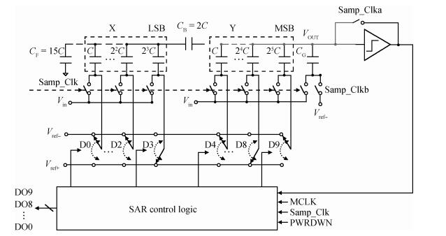
Fig. 1.
Functional block diagram of the proposed charge redistribution SAR ADC
SEMICONDUCTOR INTEGRATED CIRCUITS
Hongming Chen1, 2, , Yueguo Hao1, 2, Long Zhao1, 2 and Yuhua Cheng1, 2
Corresponding author: Chen Hongming, Email:chenhongming@shrime-pku.org.cn
Abstract: An area-efficient CMOS 1-MS/s 10-bit charge-redistribution SAR ADC for battery voltage measurement in a SoC chip is proposed. A new DAC architecture presents the benefits of a low power approach without applying the common mode voltage. The threshold inverter quantizer (TIQ)-based CMOS Inverter is used as a comparator in the ADC to avoid static power consumption which is attractive in battery-supply application. Sixteen level-up shifters aim at converting the ultra low core voltage control signals to the higher voltage level analog circuit in a 55 nm CMOS process. The whole ADC power consumption is 2.5 mW with a maximum input capacitance of 12 pF in the sampling mode. The active area of the proposed ADC is 0.0462 mm2 and it achieves the SFDR and ENOB of 65.6917 dB and 9.8726 bits respectively with an input frequency of 200 kHz at 1 MS/s sampling rate.
Keywords: successive approximation register, analog-to-digital converter, charge redistribution, threshold inverter quantizer
| [1] |
Kamalinejad P, Mirabbasi S, Leung V C M. An ultra-low-power SAR ADC with an area-efficient DAC architecture. IEEE International Symposium on Circuits and Systems (ISCAS), 2011:13 http://ieeexplore.ieee.org/document/5937489/?arnumber=5937489
|
| [2] |
Guo W, Mirabbasi S. A low-power 10-bit 50-MS/s SAR ADC using a parasitic-compensated split-capacitor DAC. IEEE International Symposium on Circuits and Systems (ISCAS), 2012:1275 http://ieeexplore.ieee.org/document/6271470/keywords
|
| [3] |
Kuo C H, Hsieh C E. A high energy-efficiency SAR ADC based on partial floating capacitor switching technique. ESSCIRC, 2011 http://ieeexplore.ieee.org/document/6045010/
|
| [4] |
Van Elzakker M, van Tuijl E, Geraedts P, et al. A 10-bit charge-redistribution ADC consuming 1.9μ W at 1 MS/s. IEEE J Solid-State Circuits, 2010, 45(5):1007 doi: 10.1109/JSSC.2010.2043893
|
| [5] |
Zhong L, Yang H, Zhang C. Design of an embedded CMOS CR SAR ADC for low power applications in bio-sensor SOC. ASICON, 2007:668 http://ieeexplore.ieee.org/document/4415719/?reload=true&arnumber=4415719&sortType%3Dasc_p_Sequence%26filter%3DAND(p_IS_Number:4415536)%26pageNumber%3D2%26rowsPerPage%3D100
|
| [6] |
Ginsburg B P, Chandrakasan A P. Highly interleaved 5-bit, 250-MSample/s, 1.2-mW ADC with redundant channels in 65-nm CMOS. IEEE J Solid-State Circuits, 2008, 43(12):2641 doi: 10.1109/JSSC.2008.2006334
|
| [7] |
McCreary J L, Gray P R. LL-MOS charge redistribution analog-to-digital conversion techniques. Part I. IEEE J Solid-State Circuits, 1975, 10(6):371 doi: 10.1109/JSSC.1975.1050629
|
| [8] |
Agnes A, Bonizzoni E, Maloberti F. Design of an ultra-low power SA-ADC with medium/high resolution and speed. IEEE International Symposium on Circuits and Systems (ISCAS), 2008
|
| [9] |
Chen Y, Zhu X, Tamura H, et al. Split capacitor DAC mismatch calibration in successive approximation ADC. IEEE Custom Integrated Circuits Conference, 2009:279
|
| [10] |
Zhu Y, Chan C H, Chio U F, et al. A voltage feedback charge compensation technique for split DAC architecture in SAR ADC. IEEE International Symposium on Circuits and Systems (ISCAS), 2010:4061
|
| [11] |
Tangel A, Choi K. The CMOS inverter as a comparator in ADC design. Analog Integrated Circuits and Signal Processing, 2003:147
|
| [12] |
Tangel A. VLSI implementation of the threshold inverter quantization (TIQ) technique for CMOS flash A/D converter applications. PhD Dissertation, The Pennsylvania State University, 1999:243
|
| [13] |
Segura J, Rossello J L, Morra J, et al. A variable threshold voltage inverter for CMOS programmable logic circuits. IEEE J Solid-State Circuits, 1998, 33(8):1262 doi: 10.1109/4.705367
|
| [14] |
Koo K H, Seo J H, Ko M L, et al. A new level-up shifter for high speed and wide range interface in ultra deep sub-micron. IEEE International Symposium on Circuits and Systems (ISCAS), 2005:1063
|
| [15] |
Tong Xingyuan, Chen Jianming, Zhu Zhangming, et al. A high performance 90 nm CMOS SAR ADC with hybrid architecture. Journal of Semiconductors, 2010, 31(1):015002 doi: 10.1088/1674-4926/31/1/015002
|
| [16] |
Zeng Z, Dong C S, Tan X. A 10-bit 1 MS/s low power SAR ADC for RSSI application. IEEE ICSICT, 2010:569
|
| [17] |
Abdelhalim K, MacEachern L, Mahmoud S. A nanowatt successive approximation ADC with offset correction for implantable sensor applications. IEEE International Symposium on Circuits and Systems (ISCAS), 2007:2351
|
| [18] |
Yang Siyu, Zhang Hui, Fu Wenhui, et al. A low power 12-bit 200-kS/s SAR ADC with a differential time domain comparator. Journal of Semiconductors, 2011, 32(3):035002 doi: 10.1088/1674-4926/32/3/035002
|
| [19] |
Wu H, Li B, Zou M, et al. An 1.2V 8-bit 1-MS/s single-input res-cap segment SAR ADC for temperature sensor in LTE. International Conference of Electron Devices and Solid-State Circuits (EDSSC), 2011
|
| [20] |
Trakimas M, Hancock T, Sonkusale S. A compressed sensing analog-to-information converter with edge-triggered SAR ADC core. IEEE International Symposium on Circuits and Systems (ISCAS), 2012:3162
|
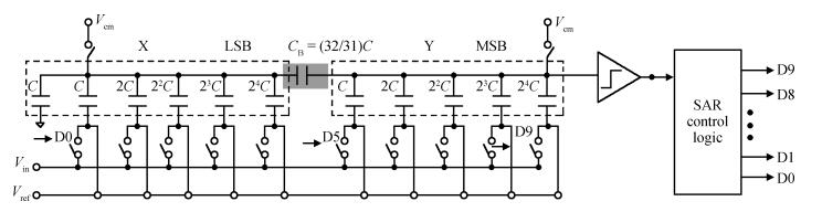
Table 1. ADC performance summary

|
Table 2. Performance comparison with previous works

|
| [1] |
Kamalinejad P, Mirabbasi S, Leung V C M. An ultra-low-power SAR ADC with an area-efficient DAC architecture. IEEE International Symposium on Circuits and Systems (ISCAS), 2011:13 http://ieeexplore.ieee.org/document/5937489/?arnumber=5937489
|
| [2] |
Guo W, Mirabbasi S. A low-power 10-bit 50-MS/s SAR ADC using a parasitic-compensated split-capacitor DAC. IEEE International Symposium on Circuits and Systems (ISCAS), 2012:1275 http://ieeexplore.ieee.org/document/6271470/keywords
|
| [3] |
Kuo C H, Hsieh C E. A high energy-efficiency SAR ADC based on partial floating capacitor switching technique. ESSCIRC, 2011 http://ieeexplore.ieee.org/document/6045010/
|
| [4] |
Van Elzakker M, van Tuijl E, Geraedts P, et al. A 10-bit charge-redistribution ADC consuming 1.9μ W at 1 MS/s. IEEE J Solid-State Circuits, 2010, 45(5):1007 doi: 10.1109/JSSC.2010.2043893
|
| [5] |
Zhong L, Yang H, Zhang C. Design of an embedded CMOS CR SAR ADC for low power applications in bio-sensor SOC. ASICON, 2007:668 http://ieeexplore.ieee.org/document/4415719/?reload=true&arnumber=4415719&sortType%3Dasc_p_Sequence%26filter%3DAND(p_IS_Number:4415536)%26pageNumber%3D2%26rowsPerPage%3D100
|
| [6] |
Ginsburg B P, Chandrakasan A P. Highly interleaved 5-bit, 250-MSample/s, 1.2-mW ADC with redundant channels in 65-nm CMOS. IEEE J Solid-State Circuits, 2008, 43(12):2641 doi: 10.1109/JSSC.2008.2006334
|
| [7] |
McCreary J L, Gray P R. LL-MOS charge redistribution analog-to-digital conversion techniques. Part I. IEEE J Solid-State Circuits, 1975, 10(6):371 doi: 10.1109/JSSC.1975.1050629
|
| [8] |
Agnes A, Bonizzoni E, Maloberti F. Design of an ultra-low power SA-ADC with medium/high resolution and speed. IEEE International Symposium on Circuits and Systems (ISCAS), 2008
|
| [9] |
Chen Y, Zhu X, Tamura H, et al. Split capacitor DAC mismatch calibration in successive approximation ADC. IEEE Custom Integrated Circuits Conference, 2009:279
|
| [10] |
Zhu Y, Chan C H, Chio U F, et al. A voltage feedback charge compensation technique for split DAC architecture in SAR ADC. IEEE International Symposium on Circuits and Systems (ISCAS), 2010:4061
|
| [11] |
Tangel A, Choi K. The CMOS inverter as a comparator in ADC design. Analog Integrated Circuits and Signal Processing, 2003:147
|
| [12] |
Tangel A. VLSI implementation of the threshold inverter quantization (TIQ) technique for CMOS flash A/D converter applications. PhD Dissertation, The Pennsylvania State University, 1999:243
|
| [13] |
Segura J, Rossello J L, Morra J, et al. A variable threshold voltage inverter for CMOS programmable logic circuits. IEEE J Solid-State Circuits, 1998, 33(8):1262 doi: 10.1109/4.705367
|
| [14] |
Koo K H, Seo J H, Ko M L, et al. A new level-up shifter for high speed and wide range interface in ultra deep sub-micron. IEEE International Symposium on Circuits and Systems (ISCAS), 2005:1063
|
| [15] |
Tong Xingyuan, Chen Jianming, Zhu Zhangming, et al. A high performance 90 nm CMOS SAR ADC with hybrid architecture. Journal of Semiconductors, 2010, 31(1):015002 doi: 10.1088/1674-4926/31/1/015002
|
| [16] |
Zeng Z, Dong C S, Tan X. A 10-bit 1 MS/s low power SAR ADC for RSSI application. IEEE ICSICT, 2010:569
|
| [17] |
Abdelhalim K, MacEachern L, Mahmoud S. A nanowatt successive approximation ADC with offset correction for implantable sensor applications. IEEE International Symposium on Circuits and Systems (ISCAS), 2007:2351
|
| [18] |
Yang Siyu, Zhang Hui, Fu Wenhui, et al. A low power 12-bit 200-kS/s SAR ADC with a differential time domain comparator. Journal of Semiconductors, 2011, 32(3):035002 doi: 10.1088/1674-4926/32/3/035002
|
| [19] |
Wu H, Li B, Zou M, et al. An 1.2V 8-bit 1-MS/s single-input res-cap segment SAR ADC for temperature sensor in LTE. International Conference of Electron Devices and Solid-State Circuits (EDSSC), 2011
|
| [20] |
Trakimas M, Hancock T, Sonkusale S. A compressed sensing analog-to-information converter with edge-triggered SAR ADC core. IEEE International Symposium on Circuits and Systems (ISCAS), 2012:3162
|


Article views: 4056 Times PDF downloads: 43 Times Cited by: 0 Times
Received: 09 February 2013 Revised: 17 April 2013 Online: Published: 01 September 2013
| Citation: |
Hongming Chen, Yueguo Hao, Long Zhao, Yuhua Cheng. An area-efficient 55 nm 10-bit 1-MS/s SAR ADC for battery voltage measurement[J]. Journal of Semiconductors, 2013, 34(9): 095013. doi: 10.1088/1674-4926/34/9/095013
****
H M Chen, Y G Hao, L Zhao, Y H Cheng. An area-efficient 55 nm 10-bit 1-MS/s SAR ADC for battery voltage measurement[J]. J. Semicond., 2013, 34(9): 095013. doi: 10.1088/1674-4926/34/9/095013.

|
| [1] |
Kamalinejad P, Mirabbasi S, Leung V C M. An ultra-low-power SAR ADC with an area-efficient DAC architecture. IEEE International Symposium on Circuits and Systems (ISCAS), 2011:13 http://ieeexplore.ieee.org/document/5937489/?arnumber=5937489
|
| [2] |
Guo W, Mirabbasi S. A low-power 10-bit 50-MS/s SAR ADC using a parasitic-compensated split-capacitor DAC. IEEE International Symposium on Circuits and Systems (ISCAS), 2012:1275 http://ieeexplore.ieee.org/document/6271470/keywords
|
| [3] |
Kuo C H, Hsieh C E. A high energy-efficiency SAR ADC based on partial floating capacitor switching technique. ESSCIRC, 2011 http://ieeexplore.ieee.org/document/6045010/
|
| [4] |
Van Elzakker M, van Tuijl E, Geraedts P, et al. A 10-bit charge-redistribution ADC consuming 1.9μ W at 1 MS/s. IEEE J Solid-State Circuits, 2010, 45(5):1007 doi: 10.1109/JSSC.2010.2043893
|
| [5] |
Zhong L, Yang H, Zhang C. Design of an embedded CMOS CR SAR ADC for low power applications in bio-sensor SOC. ASICON, 2007:668 http://ieeexplore.ieee.org/document/4415719/?reload=true&arnumber=4415719&sortType%3Dasc_p_Sequence%26filter%3DAND(p_IS_Number:4415536)%26pageNumber%3D2%26rowsPerPage%3D100
|
| [6] |
Ginsburg B P, Chandrakasan A P. Highly interleaved 5-bit, 250-MSample/s, 1.2-mW ADC with redundant channels in 65-nm CMOS. IEEE J Solid-State Circuits, 2008, 43(12):2641 doi: 10.1109/JSSC.2008.2006334
|
| [7] |
McCreary J L, Gray P R. LL-MOS charge redistribution analog-to-digital conversion techniques. Part I. IEEE J Solid-State Circuits, 1975, 10(6):371 doi: 10.1109/JSSC.1975.1050629
|
| [8] |
Agnes A, Bonizzoni E, Maloberti F. Design of an ultra-low power SA-ADC with medium/high resolution and speed. IEEE International Symposium on Circuits and Systems (ISCAS), 2008
|
| [9] |
Chen Y, Zhu X, Tamura H, et al. Split capacitor DAC mismatch calibration in successive approximation ADC. IEEE Custom Integrated Circuits Conference, 2009:279
|
| [10] |
Zhu Y, Chan C H, Chio U F, et al. A voltage feedback charge compensation technique for split DAC architecture in SAR ADC. IEEE International Symposium on Circuits and Systems (ISCAS), 2010:4061
|
| [11] |
Tangel A, Choi K. The CMOS inverter as a comparator in ADC design. Analog Integrated Circuits and Signal Processing, 2003:147
|
| [12] |
Tangel A. VLSI implementation of the threshold inverter quantization (TIQ) technique for CMOS flash A/D converter applications. PhD Dissertation, The Pennsylvania State University, 1999:243
|
| [13] |
Segura J, Rossello J L, Morra J, et al. A variable threshold voltage inverter for CMOS programmable logic circuits. IEEE J Solid-State Circuits, 1998, 33(8):1262 doi: 10.1109/4.705367
|
| [14] |
Koo K H, Seo J H, Ko M L, et al. A new level-up shifter for high speed and wide range interface in ultra deep sub-micron. IEEE International Symposium on Circuits and Systems (ISCAS), 2005:1063
|
| [15] |
Tong Xingyuan, Chen Jianming, Zhu Zhangming, et al. A high performance 90 nm CMOS SAR ADC with hybrid architecture. Journal of Semiconductors, 2010, 31(1):015002 doi: 10.1088/1674-4926/31/1/015002
|
| [16] |
Zeng Z, Dong C S, Tan X. A 10-bit 1 MS/s low power SAR ADC for RSSI application. IEEE ICSICT, 2010:569
|
| [17] |
Abdelhalim K, MacEachern L, Mahmoud S. A nanowatt successive approximation ADC with offset correction for implantable sensor applications. IEEE International Symposium on Circuits and Systems (ISCAS), 2007:2351
|
| [18] |
Yang Siyu, Zhang Hui, Fu Wenhui, et al. A low power 12-bit 200-kS/s SAR ADC with a differential time domain comparator. Journal of Semiconductors, 2011, 32(3):035002 doi: 10.1088/1674-4926/32/3/035002
|
| [19] |
Wu H, Li B, Zou M, et al. An 1.2V 8-bit 1-MS/s single-input res-cap segment SAR ADC for temperature sensor in LTE. International Conference of Electron Devices and Solid-State Circuits (EDSSC), 2011
|
| [20] |
Trakimas M, Hancock T, Sonkusale S. A compressed sensing analog-to-information converter with edge-triggered SAR ADC core. IEEE International Symposium on Circuits and Systems (ISCAS), 2012:3162
|

 WeChat ID
Journal of Semiconductors © 2017 All Rights Reserved 京ICP备05085259号-2

 DownLoad: