


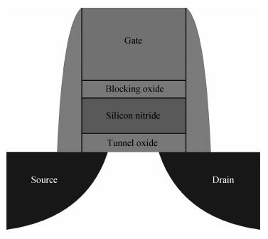
Fig. 1.
Schematic map of a SONOS device. Electrons or holes tunnel through the tunnel oxide layer into the trapping layer of silicon nitride under proper bias voltage, and then become trapped in the silicon nitride trapping layer.
SEMICONDUCTOR DEVICES
Jing Luo1, Jinlong Lu1, Hongpeng Zhao1, Yuehua Dai1, , Qi Liu2, Jin Yang1, Xianwei Jiang1 and Huifang Xu1
Corresponding author: Dai Yuehua, Email:daiyuehua2013@163.com
Abstract: Based on first principle calculations, a comprehensive study of substitutional oxygen defects in hexagonal silicon nitride (β-Si3N4) has been carried out. Firstly, it is found that substitutional oxygen is most likely to form clusters at three sites in Si3N4 due to the intense attractive interaction between oxygen defects. Then, by using three analytical tools (trap energy, modified Bader analysis and charge density difference), we discuss the trap abilities of the three clusters. The result shows that each kind of cluster at the three specific sites presents very different abilities to trap charge carriers (electrons or holes):two of the three clusters can trap both kinds of charge carriers, confirming their amphoteric property; While the last remaining one is only able to trap hole carriers. Moreover, our studies reveal that the three clusters differ from each other in terms of endurance during the program/erase progress. Taking full account of capturing properties for the three oxygen clusters, including trap ability and endurance, we deem holes rather than electrons to be optimal to act as operational charge carriers for the oxygen defects in Si3N4-based charge trapping memories.
Keywords: charge trapping memory, silicon nitride, substitutional oxygen, capturing property, first-principle
| [1] |
Kim K. Technology for sub-50 nm DRAM and NAND flash manufacturing. Electron Devices Meeting, 2005, 5(5):323
|
| [2] |
Lu C Y, Liu R. Future challenges of flash memory technologies. Microelectron Eng, 2009, 86(3):283 doi: 10.1016/j.mee.2008.08.007
|
| [3] |
Robertson J, Powell M. Gap states in silicon nitride. Appl Phys Lett, 1984, 44(4):415 doi: 10.1063/1.94794
|
| [4] |
Gritsenko V A, Nekrashevich S S, Vasilev V V, et al. Electronic structure of memory traps in silicon nitride. Microelectron Eng, 2009, 86:1866 doi: 10.1016/j.mee.2009.03.093
|
| [5] |
Vianello E, Driussi F, Perniola L, et al. Explanation of the charge-trapping properties of silicon nitride storage layers for NVM devices. Part Ⅰ: experimental evidences from physical and electrical characterizations. IEEE Trans Electron Devices, 2011, 58(8): 2483
|
| [6] |
Vianello E, Driussi F, Blaise P, et al. Explanation of the charge trapping properties of silicon nitride storage layers for NVMs. Part Ⅱ: atomistic and electrical modeling. IEEE Trans Electron Devices, 2011, 58(8): 2490
|
| [7] |
Valentin C D, Palma G, Pacchioni G. Ab initio study of transition levels for intrinsic defects in silicon nitride. J Phys Chem C, 2011, 115(2):561 doi: 10.1021/jp106756f
|
| [8] |
Kresse G, Joubert D. From ultrasoft pseudopotentials to the projector augmented-wave method. Phys Rev B, 1999, 59(3):1758 doi: 10.1103/PhysRevB.59.1758
|
| [9] |
Kresse G, Furthmüller J. Efficient iterative schemes for ab initio total-energy calculations using a plane-wave basis set. Canadian Metallurgical Quarterly, 1996, 54(16):11169
|
| [10] |
Perdew J P, Burke K, Ernzerhof M. Generalized gradient approximation made simple. Phys Rev Lett, 1997, 77(18):3865
|
| [11] |
Zhang W, Hou Z F. Interaction and electronic structures of oxygen divacancy in HfO2. Phys Status Solidi B, 2012, 250(2):352
|
| [12] |
Tang W, Sanville E, Henkelman G. A grid-based Bader analysis algorithm without lattice bias. J Phys:Condensed Matter, 2009, 21:084204 doi: 10.1088/0953-8984/21/8/084204
|
| [13] |
Edward S, Kenny S D, Smith R, et al. Improved grid-based algorithm for Bader charge allocation. Journal of Computational Chemistry, 2007, 28(5):899 doi: 10.1002/(ISSN)1096-987X
|
| [14] |
Henkelman G, Arnaldsson A, Jónsson H. A fast and robust algorithm for Bader decomposition of charge density. Computer Science Masters, 2006, 36:354 doi: 10.1016/j.commatsci.2005.04.010
|
| [15] |
Otake A, Yamaguchi K, Kmiya K, et al. An atomistic study on hydrogenation effects toward quality improvement of program/erase cycle of MONOS-type memory. IEICE Trans Electron, 2011, E94-C:693
|
| [16] |
Queisser H J, Haller E E. Defects in semiconductors:some fatal, some vital. Science (New York), 1998, 281(5379):945 doi: 10.1126/science.281.5379.945
|
| [17] |
Van de Walle, Chris G, Neugebauer J. First-principles calculations for defects and impurities:applications to Ⅲ-nitrides. J Appl Phys, 2004, 95(8):3851 doi: 10.1063/1.1682673
|
| [18] |
Henkelman G, Jónsson H. Improved tangent estimate in the nudged elastic band method for finding minimum energy paths and saddle points. J Chem Phys, 2000, 113(22):9978 doi: 10.1063/1.1323224
|
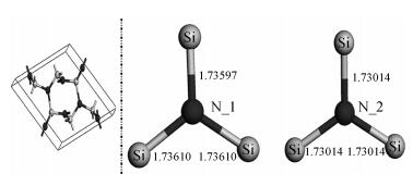
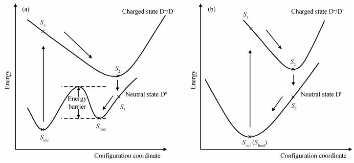
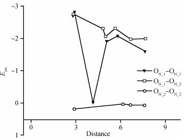
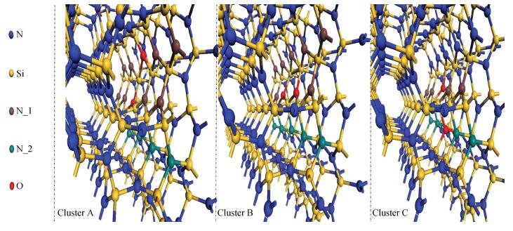
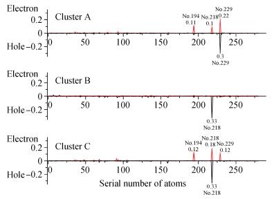
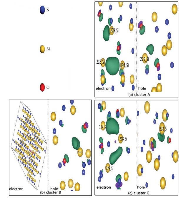
Table 1.
The calculated values for the interaction energy

|
Table 2. Calculated trap energy for charge carriers. (eV)

|
Table 3.
Result of comparison between

|
| [1] |
Kim K. Technology for sub-50 nm DRAM and NAND flash manufacturing. Electron Devices Meeting, 2005, 5(5):323
|
| [2] |
Lu C Y, Liu R. Future challenges of flash memory technologies. Microelectron Eng, 2009, 86(3):283 doi: 10.1016/j.mee.2008.08.007
|
| [3] |
Robertson J, Powell M. Gap states in silicon nitride. Appl Phys Lett, 1984, 44(4):415 doi: 10.1063/1.94794
|
| [4] |
Gritsenko V A, Nekrashevich S S, Vasilev V V, et al. Electronic structure of memory traps in silicon nitride. Microelectron Eng, 2009, 86:1866 doi: 10.1016/j.mee.2009.03.093
|
| [5] |
Vianello E, Driussi F, Perniola L, et al. Explanation of the charge-trapping properties of silicon nitride storage layers for NVM devices. Part Ⅰ: experimental evidences from physical and electrical characterizations. IEEE Trans Electron Devices, 2011, 58(8): 2483
|
| [6] |
Vianello E, Driussi F, Blaise P, et al. Explanation of the charge trapping properties of silicon nitride storage layers for NVMs. Part Ⅱ: atomistic and electrical modeling. IEEE Trans Electron Devices, 2011, 58(8): 2490
|
| [7] |
Valentin C D, Palma G, Pacchioni G. Ab initio study of transition levels for intrinsic defects in silicon nitride. J Phys Chem C, 2011, 115(2):561 doi: 10.1021/jp106756f
|
| [8] |
Kresse G, Joubert D. From ultrasoft pseudopotentials to the projector augmented-wave method. Phys Rev B, 1999, 59(3):1758 doi: 10.1103/PhysRevB.59.1758
|
| [9] |
Kresse G, Furthmüller J. Efficient iterative schemes for ab initio total-energy calculations using a plane-wave basis set. Canadian Metallurgical Quarterly, 1996, 54(16):11169
|
| [10] |
Perdew J P, Burke K, Ernzerhof M. Generalized gradient approximation made simple. Phys Rev Lett, 1997, 77(18):3865
|
| [11] |
Zhang W, Hou Z F. Interaction and electronic structures of oxygen divacancy in HfO2. Phys Status Solidi B, 2012, 250(2):352
|
| [12] |
Tang W, Sanville E, Henkelman G. A grid-based Bader analysis algorithm without lattice bias. J Phys:Condensed Matter, 2009, 21:084204 doi: 10.1088/0953-8984/21/8/084204
|
| [13] |
Edward S, Kenny S D, Smith R, et al. Improved grid-based algorithm for Bader charge allocation. Journal of Computational Chemistry, 2007, 28(5):899 doi: 10.1002/(ISSN)1096-987X
|
| [14] |
Henkelman G, Arnaldsson A, Jónsson H. A fast and robust algorithm for Bader decomposition of charge density. Computer Science Masters, 2006, 36:354 doi: 10.1016/j.commatsci.2005.04.010
|
| [15] |
Otake A, Yamaguchi K, Kmiya K, et al. An atomistic study on hydrogenation effects toward quality improvement of program/erase cycle of MONOS-type memory. IEICE Trans Electron, 2011, E94-C:693
|
| [16] |
Queisser H J, Haller E E. Defects in semiconductors:some fatal, some vital. Science (New York), 1998, 281(5379):945 doi: 10.1126/science.281.5379.945
|
| [17] |
Van de Walle, Chris G, Neugebauer J. First-principles calculations for defects and impurities:applications to Ⅲ-nitrides. J Appl Phys, 2004, 95(8):3851 doi: 10.1063/1.1682673
|
| [18] |
Henkelman G, Jónsson H. Improved tangent estimate in the nudged elastic band method for finding minimum energy paths and saddle points. J Chem Phys, 2000, 113(22):9978 doi: 10.1063/1.1323224
|


Article views: 3146 Times PDF downloads: 31 Times Cited by: 0 Times
Received: 26 June 2013 Revised: 25 July 2013 Online: Published: 01 January 2014
| Citation: |
Jing Luo, Jinlong Lu, Hongpeng Zhao, Yuehua Dai, Qi Liu, Jin Yang, Xianwei Jiang, Huifang Xu. A first-principle investigation of the oxygen defects in Si3N4-based charge trapping memories[J]. Journal of Semiconductors, 2014, 35(1): 014004. doi: 10.1088/1674-4926/35/1/014004
****
J Luo, J L Lu, H P Zhao, Y H Dai, Q Liu, J Yang, X W Jiang, H F Xu. A first-principle investigation of the oxygen defects in Si3N4-based charge trapping memories[J]. J. Semicond., 2014, 35(1): 014004. doi: 10.1088/1674-4926/35/1/014004.

|
| [1] |
Kim K. Technology for sub-50 nm DRAM and NAND flash manufacturing. Electron Devices Meeting, 2005, 5(5):323
|
| [2] |
Lu C Y, Liu R. Future challenges of flash memory technologies. Microelectron Eng, 2009, 86(3):283 doi: 10.1016/j.mee.2008.08.007
|
| [3] |
Robertson J, Powell M. Gap states in silicon nitride. Appl Phys Lett, 1984, 44(4):415 doi: 10.1063/1.94794
|
| [4] |
Gritsenko V A, Nekrashevich S S, Vasilev V V, et al. Electronic structure of memory traps in silicon nitride. Microelectron Eng, 2009, 86:1866 doi: 10.1016/j.mee.2009.03.093
|
| [5] |
Vianello E, Driussi F, Perniola L, et al. Explanation of the charge-trapping properties of silicon nitride storage layers for NVM devices. Part Ⅰ: experimental evidences from physical and electrical characterizations. IEEE Trans Electron Devices, 2011, 58(8): 2483
|
| [6] |
Vianello E, Driussi F, Blaise P, et al. Explanation of the charge trapping properties of silicon nitride storage layers for NVMs. Part Ⅱ: atomistic and electrical modeling. IEEE Trans Electron Devices, 2011, 58(8): 2490
|
| [7] |
Valentin C D, Palma G, Pacchioni G. Ab initio study of transition levels for intrinsic defects in silicon nitride. J Phys Chem C, 2011, 115(2):561 doi: 10.1021/jp106756f
|
| [8] |
Kresse G, Joubert D. From ultrasoft pseudopotentials to the projector augmented-wave method. Phys Rev B, 1999, 59(3):1758 doi: 10.1103/PhysRevB.59.1758
|
| [9] |
Kresse G, Furthmüller J. Efficient iterative schemes for ab initio total-energy calculations using a plane-wave basis set. Canadian Metallurgical Quarterly, 1996, 54(16):11169
|
| [10] |
Perdew J P, Burke K, Ernzerhof M. Generalized gradient approximation made simple. Phys Rev Lett, 1997, 77(18):3865
|
| [11] |
Zhang W, Hou Z F. Interaction and electronic structures of oxygen divacancy in HfO2. Phys Status Solidi B, 2012, 250(2):352
|
| [12] |
Tang W, Sanville E, Henkelman G. A grid-based Bader analysis algorithm without lattice bias. J Phys:Condensed Matter, 2009, 21:084204 doi: 10.1088/0953-8984/21/8/084204
|
| [13] |
Edward S, Kenny S D, Smith R, et al. Improved grid-based algorithm for Bader charge allocation. Journal of Computational Chemistry, 2007, 28(5):899 doi: 10.1002/(ISSN)1096-987X
|
| [14] |
Henkelman G, Arnaldsson A, Jónsson H. A fast and robust algorithm for Bader decomposition of charge density. Computer Science Masters, 2006, 36:354 doi: 10.1016/j.commatsci.2005.04.010
|
| [15] |
Otake A, Yamaguchi K, Kmiya K, et al. An atomistic study on hydrogenation effects toward quality improvement of program/erase cycle of MONOS-type memory. IEICE Trans Electron, 2011, E94-C:693
|
| [16] |
Queisser H J, Haller E E. Defects in semiconductors:some fatal, some vital. Science (New York), 1998, 281(5379):945 doi: 10.1126/science.281.5379.945
|
| [17] |
Van de Walle, Chris G, Neugebauer J. First-principles calculations for defects and impurities:applications to Ⅲ-nitrides. J Appl Phys, 2004, 95(8):3851 doi: 10.1063/1.1682673
|
| [18] |
Henkelman G, Jónsson H. Improved tangent estimate in the nudged elastic band method for finding minimum energy paths and saddle points. J Chem Phys, 2000, 113(22):9978 doi: 10.1063/1.1323224
|

 WeChat ID
Journal of Semiconductors © 2017 All Rights Reserved 京ICP备05085259号-2

 DownLoad:

