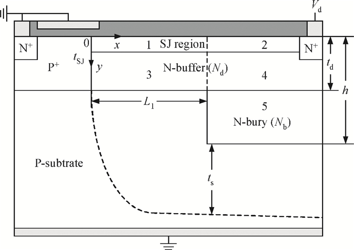
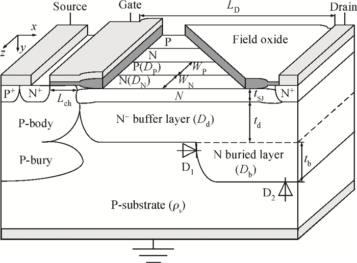
State Key Laboratory of Electronic Thin Films and Integrated Devices, University of Electronic Science and Technology of China, Chengdu 610054, ChinaState Key Laboratory of Electronic Thin Films and Integrated Devices, University of Electronic Science and Technology of China, Chengdu 610054, China
Abstract: A novel buffer super-junction (SJ) lateral double-diffused MOSFET (LDMOS) with an N-type buried layer (NB) is proposed. An N- buffer layer is implemented under the SJ region and an N-type layer is buried in the P substrate. Firstly, the new electric field peak introduced by the p-n junction of the P substrate and the N-type buried layer modulates the surface electric field distribution. Secondly, the N- buffer layer suppresses the substrate assisted depletion effect. Both of them improve the breakdown voltage (BV). Finally, because of the shallow depth of the SJ region, the NB buffer SJ-LDMOS is compatible with Bi-CMOS technology. Simulation results indicate that the average value of the surface lateral electric field strength of the NB buffer SJ-LDMOS reaches 23 V/μm at 15 μm drift length which results in a BV of 350 V and a specific on-resistance of 21 mΩ · cm2.
Lateral double-diffusion MOSFETs (LDMOS) act as an important component in power electronics applications for its facility integration. One of the main issues is the trade-off between breakdown voltage (BV) capability and specific on-resistance (Ron,sp). The super-junction (SJ) concept[1,2] used in LDMOS[3,4] further improves the trade-off between BV and Ron,sp. Unfortunately, the N pillars of the conventional SJ-LDMOST are depleted by neighboring P pillars as well as by the P substrate, while the P pillars are depleted by neighboring N pillars only, which is called the substrate-assisted depletion (SAD) effect. This effect causes a charge imbalance and results in the decrease of the BV. To alleviate the SAD effect, several new structures have been developed[5-13]. In particular, with the development of the smart power integrated circuit (SPIC), it is very crucial to design an SJ-LDMOS integrated in SPICs implementing in a CMOS-compatible process[14].
In this letter, we propose a buffer SJ-LDMOS with an N-type buried (NB) layer. The N− buffer layer suppresses the SAD effect and a more uniform surface electric field distribution is obtained due to the electric field modulation effect produced by an additional electric field peak between the P substrate and N-buried layer. The higher BV can be therefore achieved. In addition, this device is compatible with Bi-CMOS technology which can be facilely integrated in SPICs.
2.
Device structure and mechanism
The NB buffer SJ-LDMOS is illustrated in Fig. 1. An N− buffer layer is implemented under the SJ region and an N-type layer is embedded in the P substrate. Firstly, the N− buffer layer compensates the lack of charge in the N pillars caused by the depletion between the N pillars and P substrate. The N− buffer layer therefore ensures the charge balance and suppresses the SAD effect. It also enables the NB buffer SJ-LDMOS to use shallow SJ pillars. Secondly, since the N-type layer is buried in the P substrate, a new electric field peak occurs at the p-n junction of the P substrate and the N-buried layer (i.e. D1 junction in Fig. 1). This new electric field peak modulates the electric field distribution which causes a more uniform distribution of the surface electric field. It results in an improvement in BV. tSJ, td, and tb are the thickness of SJ region, N− buffer layer, and N-buried layer, respectively. WN and WP are the width of the N pillar and the P pillar. Lch and LD are the length of the channel and the drift length. DN, DP, Dd, and Db are the implantation doses of the N pillar, the P pillar, the N-buffer layer, and the N-buried layer, respectively. In this brief, tSJ= 1 μm, td=tb= 4.5 μm, h= 9 μm, WN=WP= 1 μm, Lch= 5 μm, LD= 15 μm and ρs= 65 Ω⋅cm are used, and DN=DP= 2 × 1012 cm−2 is used in Figs. 3 and 4.
Figure
1.
Three-dimensional (3D) view of the NB buffer SJ-LDMOS.
Figure
3.
Process flows of manufacture of the buried SJ layer. (a) Formation of N-buried layer. (b) Epitaxial growth and ions implantation to form N-buffer layer. (c) Gate oxide growth. (d) Ion implantation to form the SJ region.
Figure 2 illustrates the schematic cross section of the NB buffer SJ-LDMOS. The whole drift region is divided into five parts and their boundary positions are given by x=0,x=L1, x=LD and y=0,y=tSJ, y=td, y=h. When the device is biased in the off-state configuration and the drift region is fully depleted, the potential function in the silicon film must be satisfied by the 2D Poisson equation, yielding:
∂2ϕi(x,y)∂x2+∂2ϕi(x,y)∂y2=−qNiεsi,i=1,2,3,4,5,
(1)
Figure
2.
Cross-section of the NB buffer SJ-LDMOS.
Substituting Eqs. (7)-(9) into Eq. (1) under the boundary conditions (2)-(5) leads to a equation for the surface potential distribution function as follows,
∂2ϕi(x,0)∂x2−ϕi(x,0)t2i=−qNi,effεsi,i=1,2,
(10)
where N1,eff=Nd, N2,eff=Nb+(Nb−Nd)[t2d−(2h+ts)td]/2t22, t1= [(t2d+tdts)/2]1/2, t2= [(h2+hts)/2]1/2. Solving Eq. (10) with the boundary condition (6) yields the surface electric distribution as follows,
where L0= 0, L2=LD. According to Eq. (11), it is easy to find that the surface electric field distribution can be modulated by parameters Ni,eff and ti. It shows the theoretical explanation of the NB buffer SJ-LDMOS.
The key steps in the Bi-CMOS process are the formations of the N-buried layer and the surface shallow SJ pillars. The N-buried layer is realized by masked implantation of phosphorus in the P substrate before the epitaxial layer is formed on substrate. And the surface shallow SJ pillars are formed by ion implantation after field oxide formation. The main steps of one feasible fabrication method for the NB buffer SJ-LDMOS are given in Fig. 3 as follows: phosphorus ion implantation is implemented to form the N-buried layer. Lb is the length of the masking opening; epitaxial growth and phosphorus ions implantation are implemented to form an N-buffer layer; during high temperature processes in field oxide formation, the device is masked to prevent the formation of thick oxide above the N− drift region and a thick N-buffer layer is formed. Then a uniform, thin gate oxide is employed, which has a typical thickness of 200-1000 Å. One advantage of using such thin oxide is that it reduces the required energy for the ion implantation used to form the buried SJ layer; then phosphorus ions and boron ions are implanted to form the N pillar and the P pillar, respectively. The reason for forming the SJ region after field oxide formation is to avoid high temperature processes during the long time of the field oxide formation. It reduces thermal diffusion of impurities in the SJ region and suppresses dopant inter-diffusion between the P pillar and the N pillar effectively; and finally, deposit thick oxide and form the P+ contact, the N+ source/drain regions, and electrodes.
3.
Result and discussion
The three-dimensional (3D) device simulations carried out by Sentaurus[15] were performed in order to demonstrate the performances of the NB buffer SJ-LDMOS. In Fig. 4 the potential distribution for the NB buffer SJ-LDMOS, buffer SJ-LDMOS and the conventional SJ-LDMOS are compared. It is clear that the equipotential contours of the NB buffer SJ-LDMOS are evenly spaced and the depletion area extends deeper into the substrate, in comparison with those of buffer SJ-LDMOS and the conventional SJ-LDMOS. The BV of the NB buffer SJ-LDMOS reaches 350 V compared with 120 V of the conventional SJ-LDMOS, which is increased by about 190%.
Figure 5(a) shows the lateral electric field profiles at the silicon surface and at the top surface of the N-buried layer. A fair accordance between the analytical and numerical results may generally be found except the place near junctions due to the neglect of curvature of junctions in this model. The N-buffer layer suppresses the SAD effect. The surface lateral electric field distribution of the buffer SJ-LDMOS is therefore much more uniform than that of the conventional SJ-LDMOS. There is another electric field peak PK at D1 junction. Due to the electric field modulation effect of this new electric field peak, the surface lateral electric field strength of the NB buffer SJ-LDMOS in the middle of drift region is higher than that of the buffer SJ-LDMOS. Figure 5(b) shows vertical electric field distribution near the drain end. A new electric field peak (EC) is brought at the NB/substrate junction (i.e. D2 junction). Thus the D2 junction sustains a higher blocking voltage and BV can be improved.
Figure
5.
(a) Lateral electronic field distributions, (b) vertical electronic field distributions and the charge density around the drain (x= 25 μm) for the NB buffer SJ-LDMOS (350 V), buffer SJ-LDMOS (280 V), and the conventional SJ-LDMOS (130 V) at breakdown (NB buffer SJ-LDMOS: Lb= 5 μm, Dd= 7 × 1011 cm−2, Db= 2.7 × 1012 cm−2; Buffer SJ-LDMOS: Dd= 1.6 × 1012 cm−2, tSJ= 1 μm, td= 4.5 μm).
The thickness of the N− buffer layer and the N-buried layer are limited by the thermal budget of the process. The doping doses of the N− buffer layer and the N-buried layer must ensure charge balance among the N pillar, the P pillar, the N-buffer layer, the N-buried layer, and the P substrate that is
Dt=Dd+LbLDDb≈const,
(12)
where Dt is the total implantation dose, const is a constant which is equal to 1.6 × 1012 cm−2 in this brief (see Fig. 5(a)).
The influences of Dt and Lb on BV are shown in Fig. 6(a). It can be observed that the charge balance among the N pillar, the P pillar, the N-buffer layer, the N-buried layer, and the P substrate is achieved when Dt= 1.6 × 1012 cm−2. And maximum BV is obtained at Lb=LD/3. Hence, in the discussion below, the values of the Dt and the Lb are fixed at 1.6 × 1012 cm−2 and 13LD respectively. The BV as a function of Db is shown in Fig. 6(b). A well-designed Db makes the modulation effect obvious but prevents the premature breakdown at D1 or D2 junction. According to Eq. (1), the Dd decreases with the increase of the Db which leads to an increase in Ron,sp. To obtain the trade-off between BV and Ron,sp, the optimal range of the Db is 2.1 × 10¹²⩽Db⩽ 2.7 × 1012 cm−2. In Fig. 6(c) the influences of the charge imbalance of the SJ region on the BV for the NB buffer SJ-LDMOS and the conventional SJ-LDMOS are compared. The NB buffer SJ-LDMOS shows a charge balance at maximum BV, while the conventional SJ-LDMOS shows a charge imbalance of 80%. The maximum BV of the NB buffer SJ-LDMOS increases ΔV (ΔV= 120 V) compared with that of the conventional SJ-LDMOS.
Figure
6.
(a) BV versus Lb and Dt (DN=DP= 2 × 1012 cm−2). (b) BV and Ron,sp versus Db (Lb= 5 μm, Dt= 1.6 × 1012 cm−2, DN=DP= 2 × 1012 cm−2). (c) BV as a function of charge imbalance in the N pillars of the SJ region. (DP= 2 × 1012 cm−2, Lb= 5 μm, Dd= 7 × 1011 cm−2, Db= 2.7 × 1012 cm−2.)
The dependences of BV and Ron,sp on LD for the NB buffer SJ-LDMOS, the buffer SJ-LDMOS, and the conventional SJ-LDMOS are shown in Fig. 7. The values of the power figure of merit (FOM; FOM = BV2/Ron,sp) for the devices above are given in Table 1. It is found that the BV of the NB buffer SJ-LDMOS increases faster and saturates at a longer LD with the increase of LD (BV > 700 V at LD= 55 μm). And the Ron,sp of the NB buffer SJ-LDMOS is much lower than that of the conventional SJ-LDMOS. Although the Ron,sp of the NB buffer SJ-LDMOS is higher than that of the buffer SJ-LDMOS due to the lower doping concentration of N-buffer layer in the NB buffer SJ-LDMOS, the FOM value of the NB buffer SJ-LDMOS is the highest which means the performance of the NB buffer SJ-LDMOS is superior to the other bulk Si devices.
Figure
7.
Dependences of BV and Ron,sp on LD for an NB buffer SJ-LDMOS, a buffer SJ-LDMOS, and a conventional SJ-LDMOS.
A novel buffer SJ-LDMOS with an N-type buried layer is proposed and investigated by simulation. The N-buffer layer suppresses the SAD effect and the new electric field peaks caused by the N-buried layer modulates the surface electric field. The higher off-state BV is obtained. In addition, because of the shallow depth of the SJ pillars, the structure is compatible with Bi-CMOS technology. The NB buffer SJ-LDMOS exhibits an Ron,sp of 21 mΩ⋅cm2 and a BV of 350 V, yielding an FOM of 5.8 mW/cm2.
References
[1]
Chen X B, Mawby P A, Salama T. Theory of a novel voltage-sustaining layer for power devices. J Microelectron, 1998, 29(12):1005 doi: 10.1016/S0026-2692(98)00065-2
[2]
Chen X B, Wang X, Sin J K O. A novel high-voltage sustaining structure with buried oppositely doped regions. IEEE Trans Electron Devices, 2000, 47(6):1280 doi: 10.1109/16.842974
Udrea F, Popescu A, Miline W I. The 3D RESURF double-gate MOSFET:a revolutionary power device concept. Electron Lett, 1998, 34(8):808 doi: 10.1049/el:19980504
[5]
Wu W, Zhang B, Fang J, et al. High-voltage super-junction lateral double-diffused metal oxide semiconductor with a partial lightly doped pillar. Chin Phys B, 2013, 22(6):068501 doi: 10.1088/1674-1056/22/6/068501
[6]
Nassif-Khalil S G, Ander C, Salama T. Super-junction LDMOST on a silicon-on-sapphire substrate. IEEE Trans Electron Devices, 2003, 50(5):1385 doi: 10.1109/TED^2003.813460
[7]
Zhang B, Wang W, Chen W J, et al. High-voltage LDMOS with charge-balanced surface low on-resistance path layer. IEEE Electron Device Lett, 2009, 30(8):849 doi: 10.1109/LED^2009^2023541
[8]
Park I Y, Salama T. New superjunction LDMOST with n-buffer layer. IEEE Trans Electron Devices, 2006, 53(8):1909 doi: 10.1109/TED^2006.877007
[9]
Duan B X, Yang Y T, Zhang B. New superjunction LDMOS with N-type charges' compensation layer. IEEE Electron Device Lett, 2009, 30(3):305 doi: 10.1109/LED^2009^2012396
Rub M, Bar M, Deml G, et al. A 600 V 8.7Ω·mm2 lateral super-junction transistor Proc IEEE ISPSD, 2006:305
[12]
Chen W J, Zhang B, Li Z J. Optimization of super-junction SOI-LDMOS with a step doping surface-implanted layer. Semicond Sci Technol, 2007, 22(5):464 doi: 10.1088/0268-1242/22/5/002
Udrea F. State-of-the-art technologies and devices for high-voltage integrated circuits. IET Circuits Devices Syst, 2007, 1(5):357 doi: 10.1049/iet-cds:20070025
[15]
TCAD Sentaurus Manuals 2010 Version D-2010. 03
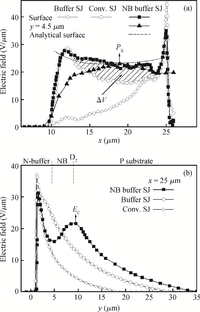
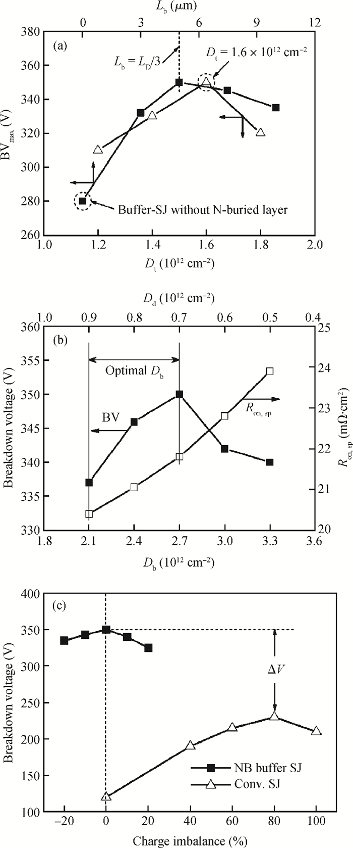
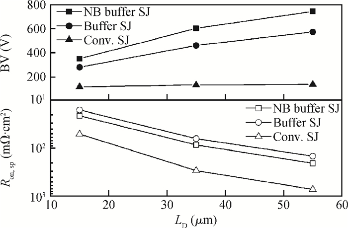
Fig. 1.
Three-dimensional (3D) view of the NB buffer SJ-LDMOS.
Fig. 3.
Process flows of manufacture of the buried SJ layer. (a) Formation of N-buried layer. (b) Epitaxial growth and ions implantation to form N-buffer layer. (c) Gate oxide growth. (d) Ion implantation to form the SJ region.
Fig. 6.
(a) BV versus Lb and Dt (DN=DP= 2 × 1012 cm−2). (b) BV and Ron,sp versus Db (Lb= 5 μm, Dt= 1.6 × 1012 cm−2, DN=DP= 2 × 1012 cm−2). (c) BV as a function of charge imbalance in the N pillars of the SJ region. (DP= 2 × 1012 cm−2, Lb= 5 μm, Dd= 7 × 1011 cm−2, Db= 2.7 × 1012 cm−2.)
Chen X B, Mawby P A, Salama T. Theory of a novel voltage-sustaining layer for power devices. J Microelectron, 1998, 29(12):1005 doi: 10.1016/S0026-2692(98)00065-2
[2]
Chen X B, Wang X, Sin J K O. A novel high-voltage sustaining structure with buried oppositely doped regions. IEEE Trans Electron Devices, 2000, 47(6):1280 doi: 10.1109/16.842974
Udrea F, Popescu A, Miline W I. The 3D RESURF double-gate MOSFET:a revolutionary power device concept. Electron Lett, 1998, 34(8):808 doi: 10.1049/el:19980504
[5]
Wu W, Zhang B, Fang J, et al. High-voltage super-junction lateral double-diffused metal oxide semiconductor with a partial lightly doped pillar. Chin Phys B, 2013, 22(6):068501 doi: 10.1088/1674-1056/22/6/068501
[6]
Nassif-Khalil S G, Ander C, Salama T. Super-junction LDMOST on a silicon-on-sapphire substrate. IEEE Trans Electron Devices, 2003, 50(5):1385 doi: 10.1109/TED^2003.813460
[7]
Zhang B, Wang W, Chen W J, et al. High-voltage LDMOS with charge-balanced surface low on-resistance path layer. IEEE Electron Device Lett, 2009, 30(8):849 doi: 10.1109/LED^2009^2023541
[8]
Park I Y, Salama T. New superjunction LDMOST with n-buffer layer. IEEE Trans Electron Devices, 2006, 53(8):1909 doi: 10.1109/TED^2006.877007
[9]
Duan B X, Yang Y T, Zhang B. New superjunction LDMOS with N-type charges' compensation layer. IEEE Electron Device Lett, 2009, 30(3):305 doi: 10.1109/LED^2009^2012396
Rub M, Bar M, Deml G, et al. A 600 V 8.7Ω·mm2 lateral super-junction transistor Proc IEEE ISPSD, 2006:305
[12]
Chen W J, Zhang B, Li Z J. Optimization of super-junction SOI-LDMOS with a step doping surface-implanted layer. Semicond Sci Technol, 2007, 22(5):464 doi: 10.1088/0268-1242/22/5/002
Udrea F. State-of-the-art technologies and devices for high-voltage integrated circuits. IET Circuits Devices Syst, 2007, 1(5):357 doi: 10.1049/iet-cds:20070025
Chinese Journal of Semiconductors , 2005, 26(12): 2286-2289.
Search
GET CITATION
Wei Wu, Bo Zhang, Jian Fang, Xiaorong Luo, Zhaoji Li. A high voltage Bi-CMOS compatible buffer super-junction LDMOS with an N-type buried layer[J]. Journal of Semiconductors, 2014, 35(1): 014009. doi: 10.1088/1674-4926/35/1/014009
W Wu, B Zhang, J Fang, X R Luo, Z J Li. A high voltage Bi-CMOS compatible buffer super-junction LDMOS with an N-type buried layer[J]. J. Semicond., 2014, 35(1): 014009. doi: 10.1088/1674-4926/35/1/014009.
Export: BibTexEndNote
Share:
Article Metrics
Article views: 3655 TimesPDF downloads: 28 TimesCited by: 0 Times
History
Received: 24 June 2013Revised: 07 September 2013Online:Published: 01 January 2014
Wei Wu, Bo Zhang, Jian Fang, Xiaorong Luo, Zhaoji Li. A high voltage Bi-CMOS compatible buffer super-junction LDMOS with an N-type buried layer[J]. Journal of Semiconductors, 2014, 35(1): 014009. doi: 10.1088/1674-4926/35/1/014009 ****W Wu, B Zhang, J Fang, X R Luo, Z J Li. A high voltage Bi-CMOS compatible buffer super-junction LDMOS with an N-type buried layer[J]. J. Semicond., 2014, 35(1): 014009. doi: 10.1088/1674-4926/35/1/014009.
Citation:
Wei Wu, Bo Zhang, Jian Fang, Xiaorong Luo, Zhaoji Li. A high voltage Bi-CMOS compatible buffer super-junction LDMOS with an N-type buried layer[J]. Journal of Semiconductors, 2014, 35(1): 014009. doi: 10.1088/1674-4926/35/1/014009
****
W Wu, B Zhang, J Fang, X R Luo, Z J Li. A high voltage Bi-CMOS compatible buffer super-junction LDMOS with an N-type buried layer[J]. J. Semicond., 2014, 35(1): 014009. doi: 10.1088/1674-4926/35/1/014009.
State Key Laboratory of Electronic Thin Films and Integrated Devices, University of Electronic Science and Technology of China, Chengdu 610054, China
Funds:
the National Defense Pre-Research of China51308020304
Project supported by the National Science and Technology Major Project of the Ministry of Science and Technology of China (No. 2010ZX02201), the National Natural Science Foundation of China (No. 61176069), and the National Defense Pre-Research of China (No. 51308020304)
the National Science and Technology Major Project of the Ministry of Science and Technology of China2010ZX02201
the National Natural Science Foundation of China61176069
A novel buffer super-junction (SJ) lateral double-diffused MOSFET (LDMOS) with an N-type buried layer (NB) is proposed. An N- buffer layer is implemented under the SJ region and an N-type layer is buried in the P substrate. Firstly, the new electric field peak introduced by the p-n junction of the P substrate and the N-type buried layer modulates the surface electric field distribution. Secondly, the N- buffer layer suppresses the substrate assisted depletion effect. Both of them improve the breakdown voltage (BV). Finally, because of the shallow depth of the SJ region, the NB buffer SJ-LDMOS is compatible with Bi-CMOS technology. Simulation results indicate that the average value of the surface lateral electric field strength of the NB buffer SJ-LDMOS reaches 23 V/μm at 15 μm drift length which results in a BV of 350 V and a specific on-resistance of 21 mΩ · cm2.
Lateral double-diffusion MOSFETs (LDMOS) act as an important component in power electronics applications for its facility integration. One of the main issues is the trade-off between breakdown voltage (BV) capability and specific on-resistance (Ron,sp). The super-junction (SJ) concept[1,2] used in LDMOS[3,4] further improves the trade-off between BV and Ron,sp. Unfortunately, the N pillars of the conventional SJ-LDMOST are depleted by neighboring P pillars as well as by the P substrate, while the P pillars are depleted by neighboring N pillars only, which is called the substrate-assisted depletion (SAD) effect. This effect causes a charge imbalance and results in the decrease of the BV. To alleviate the SAD effect, several new structures have been developed[5-13]. In particular, with the development of the smart power integrated circuit (SPIC), it is very crucial to design an SJ-LDMOS integrated in SPICs implementing in a CMOS-compatible process[14].
In this letter, we propose a buffer SJ-LDMOS with an N-type buried (NB) layer. The N− buffer layer suppresses the SAD effect and a more uniform surface electric field distribution is obtained due to the electric field modulation effect produced by an additional electric field peak between the P substrate and N-buried layer. The higher BV can be therefore achieved. In addition, this device is compatible with Bi-CMOS technology which can be facilely integrated in SPICs.
2.
Device structure and mechanism
The NB buffer SJ-LDMOS is illustrated in Fig. 1. An N− buffer layer is implemented under the SJ region and an N-type layer is embedded in the P substrate. Firstly, the N− buffer layer compensates the lack of charge in the N pillars caused by the depletion between the N pillars and P substrate. The N− buffer layer therefore ensures the charge balance and suppresses the SAD effect. It also enables the NB buffer SJ-LDMOS to use shallow SJ pillars. Secondly, since the N-type layer is buried in the P substrate, a new electric field peak occurs at the p-n junction of the P substrate and the N-buried layer (i.e. D1 junction in Fig. 1). This new electric field peak modulates the electric field distribution which causes a more uniform distribution of the surface electric field. It results in an improvement in BV. tSJ, td, and tb are the thickness of SJ region, N− buffer layer, and N-buried layer, respectively. WN and WP are the width of the N pillar and the P pillar. Lch and LD are the length of the channel and the drift length. DN, DP, Dd, and Db are the implantation doses of the N pillar, the P pillar, the N-buffer layer, and the N-buried layer, respectively. In this brief, tSJ= 1 μm, td=tb= 4.5 μm, h= 9 μm, WN=WP= 1 μm, Lch= 5 μm, LD= 15 μm and ρs= 65 Ω⋅cm are used, and DN=DP= 2 × 1012 cm−2 is used in Figs. 3 and 4.
Figure
1.
Three-dimensional (3D) view of the NB buffer SJ-LDMOS.
Figure
3.
Process flows of manufacture of the buried SJ layer. (a) Formation of N-buried layer. (b) Epitaxial growth and ions implantation to form N-buffer layer. (c) Gate oxide growth. (d) Ion implantation to form the SJ region.
Figure 2 illustrates the schematic cross section of the NB buffer SJ-LDMOS. The whole drift region is divided into five parts and their boundary positions are given by x=0,x=L1, x=LD and y=0,y=tSJ, y=td, y=h. When the device is biased in the off-state configuration and the drift region is fully depleted, the potential function in the silicon film must be satisfied by the 2D Poisson equation, yielding:
Substituting Eqs. (7)-(9) into Eq. (1) under the boundary conditions (2)-(5) leads to a equation for the surface potential distribution function as follows,
where N1,eff=Nd, N2,eff=Nb+(Nb−Nd)[t2d−(2h+ts)td]/2t22, t1= [(t2d+tdts)/2]1/2, t2= [(h2+hts)/2]1/2. Solving Eq. (10) with the boundary condition (6) yields the surface electric distribution as follows,
where L0= 0, L2=LD. According to Eq. (11), it is easy to find that the surface electric field distribution can be modulated by parameters Ni,eff and ti. It shows the theoretical explanation of the NB buffer SJ-LDMOS.
The key steps in the Bi-CMOS process are the formations of the N-buried layer and the surface shallow SJ pillars. The N-buried layer is realized by masked implantation of phosphorus in the P substrate before the epitaxial layer is formed on substrate. And the surface shallow SJ pillars are formed by ion implantation after field oxide formation. The main steps of one feasible fabrication method for the NB buffer SJ-LDMOS are given in Fig. 3 as follows: phosphorus ion implantation is implemented to form the N-buried layer. Lb is the length of the masking opening; epitaxial growth and phosphorus ions implantation are implemented to form an N-buffer layer; during high temperature processes in field oxide formation, the device is masked to prevent the formation of thick oxide above the N− drift region and a thick N-buffer layer is formed. Then a uniform, thin gate oxide is employed, which has a typical thickness of 200-1000 Å. One advantage of using such thin oxide is that it reduces the required energy for the ion implantation used to form the buried SJ layer; then phosphorus ions and boron ions are implanted to form the N pillar and the P pillar, respectively. The reason for forming the SJ region after field oxide formation is to avoid high temperature processes during the long time of the field oxide formation. It reduces thermal diffusion of impurities in the SJ region and suppresses dopant inter-diffusion between the P pillar and the N pillar effectively; and finally, deposit thick oxide and form the P+ contact, the N+ source/drain regions, and electrodes.
3.
Result and discussion
The three-dimensional (3D) device simulations carried out by Sentaurus[15] were performed in order to demonstrate the performances of the NB buffer SJ-LDMOS. In Fig. 4 the potential distribution for the NB buffer SJ-LDMOS, buffer SJ-LDMOS and the conventional SJ-LDMOS are compared. It is clear that the equipotential contours of the NB buffer SJ-LDMOS are evenly spaced and the depletion area extends deeper into the substrate, in comparison with those of buffer SJ-LDMOS and the conventional SJ-LDMOS. The BV of the NB buffer SJ-LDMOS reaches 350 V compared with 120 V of the conventional SJ-LDMOS, which is increased by about 190%.
Figure 5(a) shows the lateral electric field profiles at the silicon surface and at the top surface of the N-buried layer. A fair accordance between the analytical and numerical results may generally be found except the place near junctions due to the neglect of curvature of junctions in this model. The N-buffer layer suppresses the SAD effect. The surface lateral electric field distribution of the buffer SJ-LDMOS is therefore much more uniform than that of the conventional SJ-LDMOS. There is another electric field peak PK at D1 junction. Due to the electric field modulation effect of this new electric field peak, the surface lateral electric field strength of the NB buffer SJ-LDMOS in the middle of drift region is higher than that of the buffer SJ-LDMOS. Figure 5(b) shows vertical electric field distribution near the drain end. A new electric field peak (EC) is brought at the NB/substrate junction (i.e. D2 junction). Thus the D2 junction sustains a higher blocking voltage and BV can be improved.
Figure
5.
(a) Lateral electronic field distributions, (b) vertical electronic field distributions and the charge density around the drain (x= 25 μm) for the NB buffer SJ-LDMOS (350 V), buffer SJ-LDMOS (280 V), and the conventional SJ-LDMOS (130 V) at breakdown (NB buffer SJ-LDMOS: Lb= 5 μm, Dd= 7 × 1011 cm−2, Db= 2.7 × 1012 cm−2; Buffer SJ-LDMOS: Dd= 1.6 × 1012 cm−2, tSJ= 1 μm, td= 4.5 μm).
The thickness of the N− buffer layer and the N-buried layer are limited by the thermal budget of the process. The doping doses of the N− buffer layer and the N-buried layer must ensure charge balance among the N pillar, the P pillar, the N-buffer layer, the N-buried layer, and the P substrate that is
where Dt is the total implantation dose, const is a constant which is equal to 1.6 × 1012 cm−2 in this brief (see Fig. 5(a)).
The influences of Dt and Lb on BV are shown in Fig. 6(a). It can be observed that the charge balance among the N pillar, the P pillar, the N-buffer layer, the N-buried layer, and the P substrate is achieved when Dt= 1.6 × 1012 cm−2. And maximum BV is obtained at Lb=LD/3. Hence, in the discussion below, the values of the Dt and the Lb are fixed at 1.6 × 1012 cm−2 and 13LD respectively. The BV as a function of Db is shown in Fig. 6(b). A well-designed Db makes the modulation effect obvious but prevents the premature breakdown at D1 or D2 junction. According to Eq. (1), the Dd decreases with the increase of the Db which leads to an increase in Ron,sp. To obtain the trade-off between BV and Ron,sp, the optimal range of the Db is 2.1 × 10¹²⩽Db⩽ 2.7 × 1012 cm−2. In Fig. 6(c) the influences of the charge imbalance of the SJ region on the BV for the NB buffer SJ-LDMOS and the conventional SJ-LDMOS are compared. The NB buffer SJ-LDMOS shows a charge balance at maximum BV, while the conventional SJ-LDMOS shows a charge imbalance of 80%. The maximum BV of the NB buffer SJ-LDMOS increases ΔV (ΔV= 120 V) compared with that of the conventional SJ-LDMOS.
Figure
6.
(a) BV versus Lb and Dt (DN=DP= 2 × 1012 cm−2). (b) BV and Ron,sp versus Db (Lb= 5 μm, Dt= 1.6 × 1012 cm−2, DN=DP= 2 × 1012 cm−2). (c) BV as a function of charge imbalance in the N pillars of the SJ region. (DP= 2 × 1012 cm−2, Lb= 5 μm, Dd= 7 × 1011 cm−2, Db= 2.7 × 1012 cm−2.)
The dependences of BV and Ron,sp on LD for the NB buffer SJ-LDMOS, the buffer SJ-LDMOS, and the conventional SJ-LDMOS are shown in Fig. 7. The values of the power figure of merit (FOM; FOM = BV2/Ron,sp) for the devices above are given in Table 1. It is found that the BV of the NB buffer SJ-LDMOS increases faster and saturates at a longer LD with the increase of LD (BV > 700 V at LD= 55 μm). And the Ron,sp of the NB buffer SJ-LDMOS is much lower than that of the conventional SJ-LDMOS. Although the Ron,sp of the NB buffer SJ-LDMOS is higher than that of the buffer SJ-LDMOS due to the lower doping concentration of N-buffer layer in the NB buffer SJ-LDMOS, the FOM value of the NB buffer SJ-LDMOS is the highest which means the performance of the NB buffer SJ-LDMOS is superior to the other bulk Si devices.
Figure
7.
Dependences of BV and Ron,sp on LD for an NB buffer SJ-LDMOS, a buffer SJ-LDMOS, and a conventional SJ-LDMOS.
A novel buffer SJ-LDMOS with an N-type buried layer is proposed and investigated by simulation. The N-buffer layer suppresses the SAD effect and the new electric field peaks caused by the N-buried layer modulates the surface electric field. The higher off-state BV is obtained. In addition, because of the shallow depth of the SJ pillars, the structure is compatible with Bi-CMOS technology. The NB buffer SJ-LDMOS exhibits an Ron,sp of 21 mΩ⋅cm2 and a BV of 350 V, yielding an FOM of 5.8 mW/cm2.
Chen X B, Mawby P A, Salama T. Theory of a novel voltage-sustaining layer for power devices. J Microelectron, 1998, 29(12):1005 doi: 10.1016/S0026-2692(98)00065-2
[2]
Chen X B, Wang X, Sin J K O. A novel high-voltage sustaining structure with buried oppositely doped regions. IEEE Trans Electron Devices, 2000, 47(6):1280 doi: 10.1109/16.842974
Udrea F, Popescu A, Miline W I. The 3D RESURF double-gate MOSFET:a revolutionary power device concept. Electron Lett, 1998, 34(8):808 doi: 10.1049/el:19980504
[5]
Wu W, Zhang B, Fang J, et al. High-voltage super-junction lateral double-diffused metal oxide semiconductor with a partial lightly doped pillar. Chin Phys B, 2013, 22(6):068501 doi: 10.1088/1674-1056/22/6/068501
[6]
Nassif-Khalil S G, Ander C, Salama T. Super-junction LDMOST on a silicon-on-sapphire substrate. IEEE Trans Electron Devices, 2003, 50(5):1385 doi: 10.1109/TED^2003.813460
[7]
Zhang B, Wang W, Chen W J, et al. High-voltage LDMOS with charge-balanced surface low on-resistance path layer. IEEE Electron Device Lett, 2009, 30(8):849 doi: 10.1109/LED^2009^2023541
[8]
Park I Y, Salama T. New superjunction LDMOST with n-buffer layer. IEEE Trans Electron Devices, 2006, 53(8):1909 doi: 10.1109/TED^2006.877007
[9]
Duan B X, Yang Y T, Zhang B. New superjunction LDMOS with N-type charges' compensation layer. IEEE Electron Device Lett, 2009, 30(3):305 doi: 10.1109/LED^2009^2012396
Rub M, Bar M, Deml G, et al. A 600 V 8.7Ω·mm2 lateral super-junction transistor Proc IEEE ISPSD, 2006:305
[12]
Chen W J, Zhang B, Li Z J. Optimization of super-junction SOI-LDMOS with a step doping surface-implanted layer. Semicond Sci Technol, 2007, 22(5):464 doi: 10.1088/0268-1242/22/5/002
Udrea F. State-of-the-art technologies and devices for high-voltage integrated circuits. IET Circuits Devices Syst, 2007, 1(5):357 doi: 10.1049/iet-cds:20070025
Wei Wu, Bo Zhang, Jian Fang, Xiaorong Luo, Zhaoji Li. A high voltage Bi-CMOS compatible buffer super-junction LDMOS with an N-type buried layer[J]. Journal of Semiconductors, 2014, 35(1): 014009. doi: 10.1088/1674-4926/35/1/014009 ****W Wu, B Zhang, J Fang, X R Luo, Z J Li. A high voltage Bi-CMOS compatible buffer super-junction LDMOS with an N-type buried layer[J]. J. Semicond., 2014, 35(1): 014009. doi: 10.1088/1674-4926/35/1/014009.
Wei Wu, Bo Zhang, Jian Fang, Xiaorong Luo, Zhaoji Li. A high voltage Bi-CMOS compatible buffer super-junction LDMOS with an N-type buried layer[J]. Journal of Semiconductors, 2014, 35(1): 014009. doi: 10.1088/1674-4926/35/1/014009
****
W Wu, B Zhang, J Fang, X R Luo, Z J Li. A high voltage Bi-CMOS compatible buffer super-junction LDMOS with an N-type buried layer[J]. J. Semicond., 2014, 35(1): 014009. doi: 10.1088/1674-4926/35/1/014009.
Figure Fig. 1. Three-dimensional (3D) view of the NB buffer SJ-LDMOS.
Figure Fig. 3. Process flows of manufacture of the buried SJ layer. (a) Formation of N-buried layer. (b) Epitaxial growth and ions implantation to form N-buffer layer. (c) Gate oxide growth. (d) Ion implantation to form the SJ region.
Figure Fig. 4. The 3D equipotential contours for (a) the NB buffer SJ-LDMOS (350 V), (b) the buffer SJ-LDMOS (280 V), and (c) the conventional SJ-LDMOS (130 V) (12 V/contour. NB buffer SJ-LDMOS: Lb= 5 μm, Dd= 7 × 1011 cm−2, Db= 2.7 × 1012 cm−2; buffer SJ-LDMOS: Dd= 1.6 × 1012 cm−2, tSJ= 1 μm, td= 3.5 μm).
Figure Fig. 2. Cross-section of the NB buffer SJ-LDMOS.
Figure Fig. 5. (a) Lateral electronic field distributions, (b) vertical electronic field distributions and the charge density around the drain (x= 25 μm) for the NB buffer SJ-LDMOS (350 V), buffer SJ-LDMOS (280 V), and the conventional SJ-LDMOS (130 V) at breakdown (NB buffer SJ-LDMOS: Lb= 5 μm, Dd= 7 × 1011 cm−2, Db= 2.7 × 1012 cm−2; Buffer SJ-LDMOS: Dd= 1.6 × 1012 cm−2, tSJ= 1 μm, td= 4.5 μm).
Figure Fig. 6. (a) BV versus Lb and Dt (DN=DP= 2 × 1012 cm−2). (b) BV and Ron,sp versus Db (Lb= 5 μm, Dt= 1.6 × 1012 cm−2, DN=DP= 2 × 1012 cm−2). (c) BV as a function of charge imbalance in the N pillars of the SJ region. (DP= 2 × 1012 cm−2, Lb= 5 μm, Dd= 7 × 1011 cm−2, Db= 2.7 × 1012 cm−2.)
Figure Fig. 7. Dependences of BV and Ron,sp on LD for an NB buffer SJ-LDMOS, a buffer SJ-LDMOS, and a conventional SJ-LDMOS.