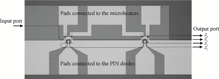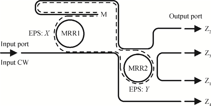
Fig. 1.
Schematic of the device. CW: continuous wave, EPS: electrical pulse signal, MRR: microring resonator.
SEMICONDUCTOR DEVICES
Fanfan Zhang, Ping Zhou, Qiaoshan Chen and Lin Yang
Corresponding author: Yang Lin, Email:oip@semi.ac.cn
Abstract: We demonstrate a directed optical decoder device consisting of two cascaded microring resonators, which are both modulated through the plasma dispersion effect. The inherent resonance wavelength mismatch between two microring resonators caused by fabrication errors is compensated for by using microheaters that are fabricated on top of the microring resonators. Two electrical signals generated by pulse pattern generators are used to modulate the PIN diodes that are embedded in the device, and the results are presented by optical signals detected at the four output ports of the device. The working wavelength and driving voltages of two MRRs are measured and analyzed by the static response spectra of the device. Dynamic experimental results show that the decoding operation is achieved at a speed of 100 Mbps.
Keywords: microring resonator, optical decoder, plasma dispersion effect
| [1] |
Hardy J, Shamir J. Optics inspired logic architecture. Opt Express, 2007, 15(1):150 doi: 10.1364/OE.15.000150
|
| [2] |
Dong P, Liao S, Feng D, et al. Low Vpp, ultralow-energy, compact, high-speed silicon electro-optic modulator. Opt Express, 2009, 17(25):22484 doi: 10.1364/OE.17.022484
|
| [3] |
Tian Y, Zhang L, Ji R, et al. Proof of concept of directed OR/NOR and AND/NAND logic circuit consisting of two parallel microring resonators. Opt Lett, 2011, 36(9):1650 doi: 10.1364/OL.36.001650
|
| [4] |
Zhang L, Ji R, Jia L, et al. Demonstration of directed XOR/XNOR logic gates using two cascaded microring resonators. Opt Lett, 2010, 35(10):1620 doi: 10.1364/OL.35.001620
|
| [5] |
Xu Q, Soref R. Reconfigurable optical directed-logic circuits using microresonator-based optical switches. Opt Express, 2011, 19(9):5244 http://cn.bing.com/academic/profile?id=aba78c7ac14036d270afdfe3e233c9bf&encoded=0&v=paper_preview&mkt=zh-cn
|
| [6] |
Xu Q, Fattal D, Beausoleil R G. Silicon microring resonators with 1.5-μm radius. Opt Express, 2008, 16(6):4309 doi: 10.1364/OE.16.004309
|
| [7] |
Zhou L, Poon A W. Electrically reconfigurable silicon microring resonator-based filter with waveguide-coupled feedback. Opt Express, 2007, 15(15):9194 doi: 10.1364/OE.15.009194
|
| [8] |
Li C, Zhou L, Poon A W. Silicon microring carrier-injection-based modulators/switches with tunable extinction ratios and OR-logic switching by using waveguide cross-coupling. Opt Express, 2007, 15(8):5069 doi: 10.1364/OE.15.005069
|
| [9] |
Soref R. Reconfigurable integrated optoelectronics. Advances in OptoElectronics, 2011, 2011:627802 http://cn.bing.com/academic/profile?id=8dda2c6759ef7142b81a2ca96bbeaa86&encoded=0&v=paper_preview&mkt=zh-cn
|
| [10] |
Cho S Y, Soref R. Interferometric microring-resonant 2×2 optical switches. Opt Express, 2008, 16(17):13304 doi: 10.1364/OE.16.013304
|
| [11] |
Shamir J. Half a century of optics in computing a personal perspective. Appl Opt, 2013, 52(4):600 doi: 10.1364/AO.52.000600
|
| [12] |
Tian Y, Zhang L, Ji R, et al. Demonstration of a directed optical decoder using two cascaded micoring resonantors. Opt Lett, 2011, 36(17):3314 doi: 10.1364/OL.36.003314
|
| [13] |
Ji R, Yang L, Zhang L, et al. Microring-resonator-based four-port optical router for photonic networks-on-chip. Opt Express, 2011, 19(20):18945 doi: 10.1364/OE.19.018945
|
| [14] |
Lu Y, Tian Y, Yang L. Integrated reconfigurable optical add-drop multiplexers based on cascaded microring resonators. Journal of Semiconductors, 2013, 34(9):094012 doi: 10.1088/1674-4926/34/9/094012
|
| [15] |
Wang Y, Qin Z, Wang C, et al. Analysis of characteristics of vertical coupling microring resonator. Journal of Semiconductors, 2012, 34(7):070412 http://www.jos.ac.cn/bdtxbcn/ch/reader/view_abstract.aspx?file_no=12120307&flag=1
|
| [16] |
Xu Q, Schmidt B, Pradhan S, et al. Micrometre-scale silicon electro-optic modulator. Nature, 2005, 435:325 doi: 10.1038/nature03569
|
| [17] |
Hu Y, Xiao X, Xu H, et al. High-speed silicon modulator based on cascaded microring resonators. Opt Express, 2012, 20(14):15079. doi: 10.1364/OE.20.015079
|
| [18] |
Ding J, Ji R, Zhang L, et al. Electro-optical response analysis of a 40 Gb/s silicon mach-zehnder optical modulator. J Lightwave Technol, 2013, 31(14):2434 doi: 10.1109/JLT.2013.2262522
|
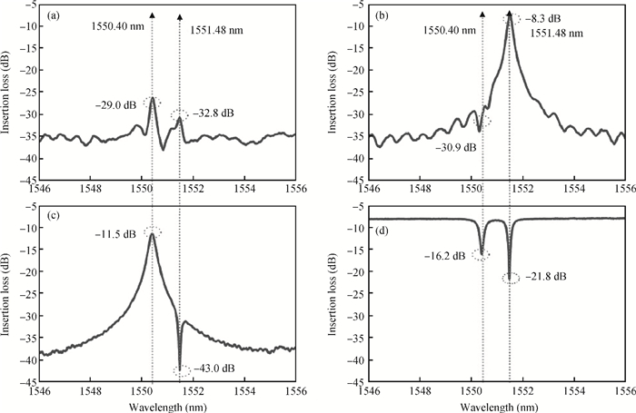
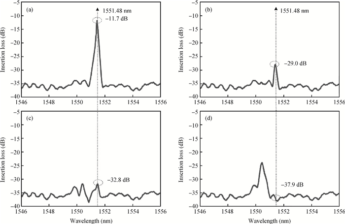
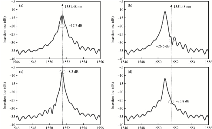
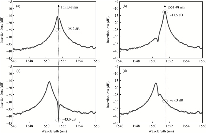
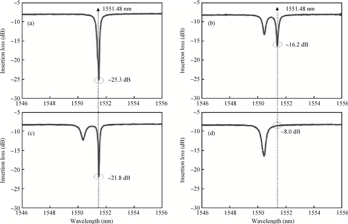
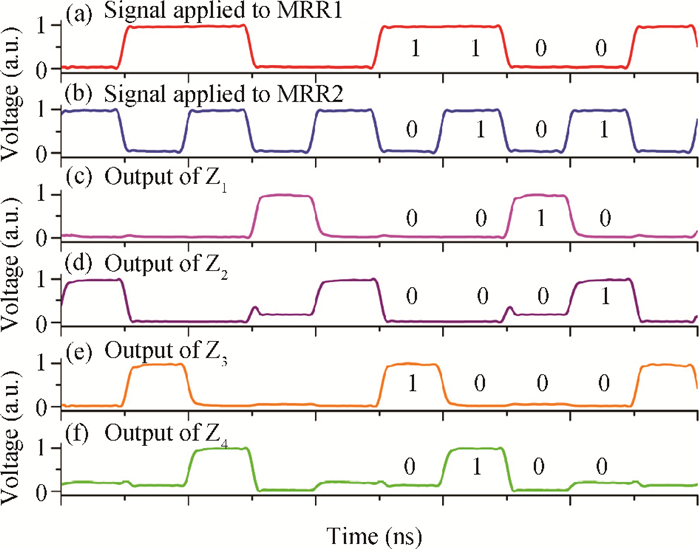
Table 1. Statuses of the device.

|
| [1] |
Hardy J, Shamir J. Optics inspired logic architecture. Opt Express, 2007, 15(1):150 doi: 10.1364/OE.15.000150
|
| [2] |
Dong P, Liao S, Feng D, et al. Low Vpp, ultralow-energy, compact, high-speed silicon electro-optic modulator. Opt Express, 2009, 17(25):22484 doi: 10.1364/OE.17.022484
|
| [3] |
Tian Y, Zhang L, Ji R, et al. Proof of concept of directed OR/NOR and AND/NAND logic circuit consisting of two parallel microring resonators. Opt Lett, 2011, 36(9):1650 doi: 10.1364/OL.36.001650
|
| [4] |
Zhang L, Ji R, Jia L, et al. Demonstration of directed XOR/XNOR logic gates using two cascaded microring resonators. Opt Lett, 2010, 35(10):1620 doi: 10.1364/OL.35.001620
|
| [5] |
Xu Q, Soref R. Reconfigurable optical directed-logic circuits using microresonator-based optical switches. Opt Express, 2011, 19(9):5244 http://cn.bing.com/academic/profile?id=aba78c7ac14036d270afdfe3e233c9bf&encoded=0&v=paper_preview&mkt=zh-cn
|
| [6] |
Xu Q, Fattal D, Beausoleil R G. Silicon microring resonators with 1.5-μm radius. Opt Express, 2008, 16(6):4309 doi: 10.1364/OE.16.004309
|
| [7] |
Zhou L, Poon A W. Electrically reconfigurable silicon microring resonator-based filter with waveguide-coupled feedback. Opt Express, 2007, 15(15):9194 doi: 10.1364/OE.15.009194
|
| [8] |
Li C, Zhou L, Poon A W. Silicon microring carrier-injection-based modulators/switches with tunable extinction ratios and OR-logic switching by using waveguide cross-coupling. Opt Express, 2007, 15(8):5069 doi: 10.1364/OE.15.005069
|
| [9] |
Soref R. Reconfigurable integrated optoelectronics. Advances in OptoElectronics, 2011, 2011:627802 http://cn.bing.com/academic/profile?id=8dda2c6759ef7142b81a2ca96bbeaa86&encoded=0&v=paper_preview&mkt=zh-cn
|
| [10] |
Cho S Y, Soref R. Interferometric microring-resonant 2×2 optical switches. Opt Express, 2008, 16(17):13304 doi: 10.1364/OE.16.013304
|
| [11] |
Shamir J. Half a century of optics in computing a personal perspective. Appl Opt, 2013, 52(4):600 doi: 10.1364/AO.52.000600
|
| [12] |
Tian Y, Zhang L, Ji R, et al. Demonstration of a directed optical decoder using two cascaded micoring resonantors. Opt Lett, 2011, 36(17):3314 doi: 10.1364/OL.36.003314
|
| [13] |
Ji R, Yang L, Zhang L, et al. Microring-resonator-based four-port optical router for photonic networks-on-chip. Opt Express, 2011, 19(20):18945 doi: 10.1364/OE.19.018945
|
| [14] |
Lu Y, Tian Y, Yang L. Integrated reconfigurable optical add-drop multiplexers based on cascaded microring resonators. Journal of Semiconductors, 2013, 34(9):094012 doi: 10.1088/1674-4926/34/9/094012
|
| [15] |
Wang Y, Qin Z, Wang C, et al. Analysis of characteristics of vertical coupling microring resonator. Journal of Semiconductors, 2012, 34(7):070412 http://www.jos.ac.cn/bdtxbcn/ch/reader/view_abstract.aspx?file_no=12120307&flag=1
|
| [16] |
Xu Q, Schmidt B, Pradhan S, et al. Micrometre-scale silicon electro-optic modulator. Nature, 2005, 435:325 doi: 10.1038/nature03569
|
| [17] |
Hu Y, Xiao X, Xu H, et al. High-speed silicon modulator based on cascaded microring resonators. Opt Express, 2012, 20(14):15079. doi: 10.1364/OE.20.015079
|
| [18] |
Ding J, Ji R, Zhang L, et al. Electro-optical response analysis of a 40 Gb/s silicon mach-zehnder optical modulator. J Lightwave Technol, 2013, 31(14):2434 doi: 10.1109/JLT.2013.2262522
|


Article views: 3033 Times PDF downloads: 9 Times Cited by: 0 Times
Received: 05 March 2014 Revised: 14 April 2014 Online: Published: 01 October 2014
| Citation: |
Fanfan Zhang, Ping Zhou, Qiaoshan Chen, Lin Yang. An electro-optic directed decoder based on two cascaded microring resonators[J]. Journal of Semiconductors, 2014, 35(10): 104011. doi: 10.1088/1674-4926/35/10/104011
****
F F Zhang, P Zhou, Q S Chen, L Yang. An electro-optic directed decoder based on two cascaded microring resonators[J]. J. Semicond., 2014, 35(10): 104011. doi: 10.1088/1674-4926/35/10/104011.

|
| [1] |
Hardy J, Shamir J. Optics inspired logic architecture. Opt Express, 2007, 15(1):150 doi: 10.1364/OE.15.000150
|
| [2] |
Dong P, Liao S, Feng D, et al. Low Vpp, ultralow-energy, compact, high-speed silicon electro-optic modulator. Opt Express, 2009, 17(25):22484 doi: 10.1364/OE.17.022484
|
| [3] |
Tian Y, Zhang L, Ji R, et al. Proof of concept of directed OR/NOR and AND/NAND logic circuit consisting of two parallel microring resonators. Opt Lett, 2011, 36(9):1650 doi: 10.1364/OL.36.001650
|
| [4] |
Zhang L, Ji R, Jia L, et al. Demonstration of directed XOR/XNOR logic gates using two cascaded microring resonators. Opt Lett, 2010, 35(10):1620 doi: 10.1364/OL.35.001620
|
| [5] |
Xu Q, Soref R. Reconfigurable optical directed-logic circuits using microresonator-based optical switches. Opt Express, 2011, 19(9):5244 http://cn.bing.com/academic/profile?id=aba78c7ac14036d270afdfe3e233c9bf&encoded=0&v=paper_preview&mkt=zh-cn
|
| [6] |
Xu Q, Fattal D, Beausoleil R G. Silicon microring resonators with 1.5-μm radius. Opt Express, 2008, 16(6):4309 doi: 10.1364/OE.16.004309
|
| [7] |
Zhou L, Poon A W. Electrically reconfigurable silicon microring resonator-based filter with waveguide-coupled feedback. Opt Express, 2007, 15(15):9194 doi: 10.1364/OE.15.009194
|
| [8] |
Li C, Zhou L, Poon A W. Silicon microring carrier-injection-based modulators/switches with tunable extinction ratios and OR-logic switching by using waveguide cross-coupling. Opt Express, 2007, 15(8):5069 doi: 10.1364/OE.15.005069
|
| [9] |
Soref R. Reconfigurable integrated optoelectronics. Advances in OptoElectronics, 2011, 2011:627802 http://cn.bing.com/academic/profile?id=8dda2c6759ef7142b81a2ca96bbeaa86&encoded=0&v=paper_preview&mkt=zh-cn
|
| [10] |
Cho S Y, Soref R. Interferometric microring-resonant 2×2 optical switches. Opt Express, 2008, 16(17):13304 doi: 10.1364/OE.16.013304
|
| [11] |
Shamir J. Half a century of optics in computing a personal perspective. Appl Opt, 2013, 52(4):600 doi: 10.1364/AO.52.000600
|
| [12] |
Tian Y, Zhang L, Ji R, et al. Demonstration of a directed optical decoder using two cascaded micoring resonantors. Opt Lett, 2011, 36(17):3314 doi: 10.1364/OL.36.003314
|
| [13] |
Ji R, Yang L, Zhang L, et al. Microring-resonator-based four-port optical router for photonic networks-on-chip. Opt Express, 2011, 19(20):18945 doi: 10.1364/OE.19.018945
|
| [14] |
Lu Y, Tian Y, Yang L. Integrated reconfigurable optical add-drop multiplexers based on cascaded microring resonators. Journal of Semiconductors, 2013, 34(9):094012 doi: 10.1088/1674-4926/34/9/094012
|
| [15] |
Wang Y, Qin Z, Wang C, et al. Analysis of characteristics of vertical coupling microring resonator. Journal of Semiconductors, 2012, 34(7):070412 http://www.jos.ac.cn/bdtxbcn/ch/reader/view_abstract.aspx?file_no=12120307&flag=1
|
| [16] |
Xu Q, Schmidt B, Pradhan S, et al. Micrometre-scale silicon electro-optic modulator. Nature, 2005, 435:325 doi: 10.1038/nature03569
|
| [17] |
Hu Y, Xiao X, Xu H, et al. High-speed silicon modulator based on cascaded microring resonators. Opt Express, 2012, 20(14):15079. doi: 10.1364/OE.20.015079
|
| [18] |
Ding J, Ji R, Zhang L, et al. Electro-optical response analysis of a 40 Gb/s silicon mach-zehnder optical modulator. J Lightwave Technol, 2013, 31(14):2434 doi: 10.1109/JLT.2013.2262522
|

 WeChat ID
Journal of Semiconductors © 2017 All Rights Reserved 京ICP备05085259号-2

 DownLoad: