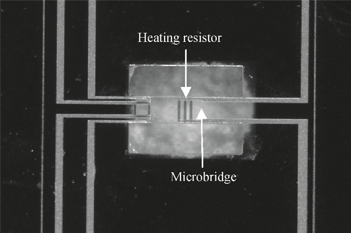
Fig. 1.
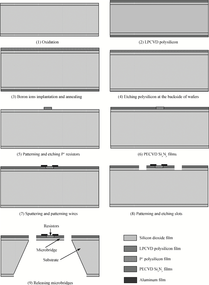
The fabrication process of a microbridge structure.
SEMICONDUCTOR TECHNOLOGY
Jianqiang Han, Yan Li, Senlin Li and Qing Li
Corresponding author: Han Jianqiang, Email:hjqsmx@sina.com
Abstract: In order to balance the compressive stress of a silicon dioxide film and compose a steady MEMS structure, a silicon-rich silicon nitride film with tensile stress is deposited by plasma enhanced chemical vapor deposition process. Accurately measuring the thermal conductivity of the film is highly desirable in order to design, simulate and optimize MEMS devices. In this paper, a SiO2/SixNy bimaterial microbridge structure is presented to measure the thermal conductivity of the silicon-rich silicon nitride film by single steady-state measurement. The thermal conductivity is extracted as 3.25 W/(m· K). Low thermal conductivity indicates that the silicon-rich silicon nitride film can still be utilized as thermally insulating material in thermal sensors although its thermal conductivity is slightly larger than the values reported in literature.
Keywords: MEMS, silicon nitride film, thermal conductivity, bimaterial microbridge
| [1] |
Chen Dapeng, Ye Tianchun, Xie Changqing, et al, Stress in SiNx film embedded with silicon nanocrystals preparing by LPCVD. Chinese Journal of Semiconductors, 2001, 22(12):1529 http://en.cnki.com.cn/Article_en/CJFDTotal-BDTX200112009.htm
|
| [2] |
Eriksson P, Andersson J Y, Stemme G. Thermal characterization of surface-micromachined silicon nitride membranes for thermal infrared detectors. J Microelectromechan Syst, 1997, 6(1):55 doi: 10.1109/84.557531
|
| [3] |
Von Arx M, Paul O, Baltes H. Process-dependent thin-film thermal conductivities for thermal CMOS MEMS. J Microelectromechan Syst, 2000, 9(1):136 doi: 10.1109/84.825788
|
| [4] |
Beigelbeck R, Kohl F, Keplinger F, et al. A novel characterization method for thermal thin-film properties applied to PECVD silicon nitride. IEEE Sensors Conference, 2007:938 http://ieeexplore.ieee.org/xpl/abstractAuthors.jsp?reload=true&arnumber=4388557
|
| [5] |
Stojanovic N, Yun J, Washington E B K, et al, Thin-film thermal conductivity measurement using microelectrothermal test structures and finite-element-model-based data analysis. J Microelectromechan Syst, 2007, 16(5):1269 doi: 10.1109/JMEMS.2007.900877
|
| [6] |
Kuntner J, Jachimowicz A, Kohl F, et al. Determining the thin-film thermal conductivity of low temperature PECVD silicon nitride. Proc Eurosensors XX, Ⅱ, 2006:388 https://www.researchgate.net/publication/229006939_Determining_the_thin_film_thermal_conductivity_of_low_temperature_pecvd_silicon_nitride
|
| [7] |
Sabat N, Santander J, Grhcia I, et al. Thermal conductivity determination of micromachined membranes. Spanish Conference on Electron Devices, 2005:229 http://ieeexplore.ieee.org/xpls/icp.jsp?arnumber=1504364
|
| [8] |
Ma Lianxiang, Duan Zhanli, He Yan, et al. The experimental study on none-equilibrium thermal conductivity of silicon nitride nano thin film. Cryo & Supercond, 2008, 36(8):92 http://en.cnki.com.cn/Article_en/CJFDTotal-DWYC200808019.htm
|
| [9] |
Shu B, Zhang H, Xuan R, et al, Fabrication of high compressive stress silicon nitride membrane in strained silicon technology. IEEE International Conference of Electron Devices and Solid-State Circuits, 2009:365 http://ieeexplore.ieee.org/document/5394243/
|
| [10] |
Nie Meng, Huang Qing'an, Li Weihua. An in-situ extracting method for residual stresses of a multilayer film by full-field optical measurement. Chinese Journal of Semiconductors, 2004, 25(5):1028 https://www.researchgate.net/publication/288438606_In-situ_extracting_method_for_residual_stresses_of_a_multilayer_film_by_full-field_optical_measurement
|
| [11] |
Xu Danqing, Yu Ying. Study on the silicon nitride film in MEMS switches. Journal of Fuzhou University (Natural Science Edition), 2009, 37(1):50 http://en.cnki.com.cn/article_en/cjfdtotal-fzdz200901011.htm
|
| [12] |
Mo Jinghui, Liu Liming, Tai Yunjian, et al. Preparation and properties of silicon nitride supporting membranes grown by plasma enhanced chemical vapor deposition. Semicond Optoelectron, 2007, 28(6):804 https://www.researchgate.net/publication/295376699_Preparation_and_properties_of_silicon_nitride_supporting_membranes_grown_by_plasma-enhanced_chemical_vapor_deposition
|
| [13] |
Ong P L, Wei J, Tay F E H, et al. A new fabrication method for low stress PECVD-SiNx layers. J Phys:Conference Series, 2006, 34:764 doi: 10.1088/1742-6596/34/1/126
|
| [14] |
Han J, Wang X, Liu Z, et al. Study on the stress of silicon nitride film deposited by PECVD. Journal of Functional Materials and Devices, 2011, 17(2):183 http://en.cnki.com.cn/Article_en/CJFDTOTAL-GNCQ201102012.htm
|
| [15] |
Xu Gaobin, Huang Qing'an. Design and simulation of on-line test structure for thermal conductivity of polysilicon thin films. Chinese Journal of Semiconductors, 2004, 25(4):430 http://en.cnki.com.cn/Article_en/CJFDTOTAL-BDTX200404013.htm
|
| [16] |
Han Jianqiang, Zhu Changchun, Liu Junhua, et al. Temperature distribution and resonance amplitude of thermally excited micromechanical beam resonators. Journal of Xi'an Jiaotong University, 2002, 36(6):592 http://en.cnki.com.cn/Article_en/CJFDTOTAL-XAJT200206010.htm
|
| [17] |
Lide D R. CRC handbook of chemistry and physics. 86th ed. New York: Taylor & Francis, 2005
|
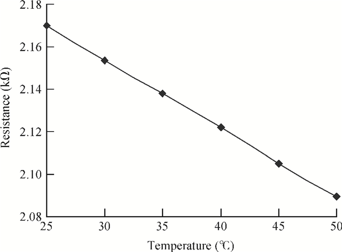
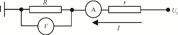
Table 1. The geometry of microbridge, measured voltage and current, calculated resistance of heating resistor.

|
| [1] |
Chen Dapeng, Ye Tianchun, Xie Changqing, et al, Stress in SiNx film embedded with silicon nanocrystals preparing by LPCVD. Chinese Journal of Semiconductors, 2001, 22(12):1529 http://en.cnki.com.cn/Article_en/CJFDTotal-BDTX200112009.htm
|
| [2] |
Eriksson P, Andersson J Y, Stemme G. Thermal characterization of surface-micromachined silicon nitride membranes for thermal infrared detectors. J Microelectromechan Syst, 1997, 6(1):55 doi: 10.1109/84.557531
|
| [3] |
Von Arx M, Paul O, Baltes H. Process-dependent thin-film thermal conductivities for thermal CMOS MEMS. J Microelectromechan Syst, 2000, 9(1):136 doi: 10.1109/84.825788
|
| [4] |
Beigelbeck R, Kohl F, Keplinger F, et al. A novel characterization method for thermal thin-film properties applied to PECVD silicon nitride. IEEE Sensors Conference, 2007:938 http://ieeexplore.ieee.org/xpl/abstractAuthors.jsp?reload=true&arnumber=4388557
|
| [5] |
Stojanovic N, Yun J, Washington E B K, et al, Thin-film thermal conductivity measurement using microelectrothermal test structures and finite-element-model-based data analysis. J Microelectromechan Syst, 2007, 16(5):1269 doi: 10.1109/JMEMS.2007.900877
|
| [6] |
Kuntner J, Jachimowicz A, Kohl F, et al. Determining the thin-film thermal conductivity of low temperature PECVD silicon nitride. Proc Eurosensors XX, Ⅱ, 2006:388 https://www.researchgate.net/publication/229006939_Determining_the_thin_film_thermal_conductivity_of_low_temperature_pecvd_silicon_nitride
|
| [7] |
Sabat N, Santander J, Grhcia I, et al. Thermal conductivity determination of micromachined membranes. Spanish Conference on Electron Devices, 2005:229 http://ieeexplore.ieee.org/xpls/icp.jsp?arnumber=1504364
|
| [8] |
Ma Lianxiang, Duan Zhanli, He Yan, et al. The experimental study on none-equilibrium thermal conductivity of silicon nitride nano thin film. Cryo & Supercond, 2008, 36(8):92 http://en.cnki.com.cn/Article_en/CJFDTotal-DWYC200808019.htm
|
| [9] |
Shu B, Zhang H, Xuan R, et al, Fabrication of high compressive stress silicon nitride membrane in strained silicon technology. IEEE International Conference of Electron Devices and Solid-State Circuits, 2009:365 http://ieeexplore.ieee.org/document/5394243/
|
| [10] |
Nie Meng, Huang Qing'an, Li Weihua. An in-situ extracting method for residual stresses of a multilayer film by full-field optical measurement. Chinese Journal of Semiconductors, 2004, 25(5):1028 https://www.researchgate.net/publication/288438606_In-situ_extracting_method_for_residual_stresses_of_a_multilayer_film_by_full-field_optical_measurement
|
| [11] |
Xu Danqing, Yu Ying. Study on the silicon nitride film in MEMS switches. Journal of Fuzhou University (Natural Science Edition), 2009, 37(1):50 http://en.cnki.com.cn/article_en/cjfdtotal-fzdz200901011.htm
|
| [12] |
Mo Jinghui, Liu Liming, Tai Yunjian, et al. Preparation and properties of silicon nitride supporting membranes grown by plasma enhanced chemical vapor deposition. Semicond Optoelectron, 2007, 28(6):804 https://www.researchgate.net/publication/295376699_Preparation_and_properties_of_silicon_nitride_supporting_membranes_grown_by_plasma-enhanced_chemical_vapor_deposition
|
| [13] |
Ong P L, Wei J, Tay F E H, et al. A new fabrication method for low stress PECVD-SiNx layers. J Phys:Conference Series, 2006, 34:764 doi: 10.1088/1742-6596/34/1/126
|
| [14] |
Han J, Wang X, Liu Z, et al. Study on the stress of silicon nitride film deposited by PECVD. Journal of Functional Materials and Devices, 2011, 17(2):183 http://en.cnki.com.cn/Article_en/CJFDTOTAL-GNCQ201102012.htm
|
| [15] |
Xu Gaobin, Huang Qing'an. Design and simulation of on-line test structure for thermal conductivity of polysilicon thin films. Chinese Journal of Semiconductors, 2004, 25(4):430 http://en.cnki.com.cn/Article_en/CJFDTOTAL-BDTX200404013.htm
|
| [16] |
Han Jianqiang, Zhu Changchun, Liu Junhua, et al. Temperature distribution and resonance amplitude of thermally excited micromechanical beam resonators. Journal of Xi'an Jiaotong University, 2002, 36(6):592 http://en.cnki.com.cn/Article_en/CJFDTOTAL-XAJT200206010.htm
|
| [17] |
Lide D R. CRC handbook of chemistry and physics. 86th ed. New York: Taylor & Francis, 2005
|


Article views: 4103 Times PDF downloads: 99 Times Cited by: 0 Times
Received: 04 September 2013 Revised: 19 November 2013 Online: Published: 01 April 2014
| Citation: |
Jianqiang Han, Yan Li, Senlin Li, Qing Li. Thermal conductivity of PECVD silicon-rich silicon nitride films measured with a SiO2/SixNy bimaterial microbridge test structure[J]. Journal of Semiconductors, 2014, 35(4): 046002. doi: 10.1088/1674-4926/35/4/046002
****
J Q Han, Y Li, S L Li, Q Li. Thermal conductivity of PECVD silicon-rich silicon nitride films measured with a SiO2/SixNy bimaterial microbridge test structure[J]. J. Semicond., 2014, 35(4): 046002. doi: 10.1088/1674-4926/35/4/046002.

|
| [1] |
Chen Dapeng, Ye Tianchun, Xie Changqing, et al, Stress in SiNx film embedded with silicon nanocrystals preparing by LPCVD. Chinese Journal of Semiconductors, 2001, 22(12):1529 http://en.cnki.com.cn/Article_en/CJFDTotal-BDTX200112009.htm
|
| [2] |
Eriksson P, Andersson J Y, Stemme G. Thermal characterization of surface-micromachined silicon nitride membranes for thermal infrared detectors. J Microelectromechan Syst, 1997, 6(1):55 doi: 10.1109/84.557531
|
| [3] |
Von Arx M, Paul O, Baltes H. Process-dependent thin-film thermal conductivities for thermal CMOS MEMS. J Microelectromechan Syst, 2000, 9(1):136 doi: 10.1109/84.825788
|
| [4] |
Beigelbeck R, Kohl F, Keplinger F, et al. A novel characterization method for thermal thin-film properties applied to PECVD silicon nitride. IEEE Sensors Conference, 2007:938 http://ieeexplore.ieee.org/xpl/abstractAuthors.jsp?reload=true&arnumber=4388557
|
| [5] |
Stojanovic N, Yun J, Washington E B K, et al, Thin-film thermal conductivity measurement using microelectrothermal test structures and finite-element-model-based data analysis. J Microelectromechan Syst, 2007, 16(5):1269 doi: 10.1109/JMEMS.2007.900877
|
| [6] |
Kuntner J, Jachimowicz A, Kohl F, et al. Determining the thin-film thermal conductivity of low temperature PECVD silicon nitride. Proc Eurosensors XX, Ⅱ, 2006:388 https://www.researchgate.net/publication/229006939_Determining_the_thin_film_thermal_conductivity_of_low_temperature_pecvd_silicon_nitride
|
| [7] |
Sabat N, Santander J, Grhcia I, et al. Thermal conductivity determination of micromachined membranes. Spanish Conference on Electron Devices, 2005:229 http://ieeexplore.ieee.org/xpls/icp.jsp?arnumber=1504364
|
| [8] |
Ma Lianxiang, Duan Zhanli, He Yan, et al. The experimental study on none-equilibrium thermal conductivity of silicon nitride nano thin film. Cryo & Supercond, 2008, 36(8):92 http://en.cnki.com.cn/Article_en/CJFDTotal-DWYC200808019.htm
|
| [9] |
Shu B, Zhang H, Xuan R, et al, Fabrication of high compressive stress silicon nitride membrane in strained silicon technology. IEEE International Conference of Electron Devices and Solid-State Circuits, 2009:365 http://ieeexplore.ieee.org/document/5394243/
|
| [10] |
Nie Meng, Huang Qing'an, Li Weihua. An in-situ extracting method for residual stresses of a multilayer film by full-field optical measurement. Chinese Journal of Semiconductors, 2004, 25(5):1028 https://www.researchgate.net/publication/288438606_In-situ_extracting_method_for_residual_stresses_of_a_multilayer_film_by_full-field_optical_measurement
|
| [11] |
Xu Danqing, Yu Ying. Study on the silicon nitride film in MEMS switches. Journal of Fuzhou University (Natural Science Edition), 2009, 37(1):50 http://en.cnki.com.cn/article_en/cjfdtotal-fzdz200901011.htm
|
| [12] |
Mo Jinghui, Liu Liming, Tai Yunjian, et al. Preparation and properties of silicon nitride supporting membranes grown by plasma enhanced chemical vapor deposition. Semicond Optoelectron, 2007, 28(6):804 https://www.researchgate.net/publication/295376699_Preparation_and_properties_of_silicon_nitride_supporting_membranes_grown_by_plasma-enhanced_chemical_vapor_deposition
|
| [13] |
Ong P L, Wei J, Tay F E H, et al. A new fabrication method for low stress PECVD-SiNx layers. J Phys:Conference Series, 2006, 34:764 doi: 10.1088/1742-6596/34/1/126
|
| [14] |
Han J, Wang X, Liu Z, et al. Study on the stress of silicon nitride film deposited by PECVD. Journal of Functional Materials and Devices, 2011, 17(2):183 http://en.cnki.com.cn/Article_en/CJFDTOTAL-GNCQ201102012.htm
|
| [15] |
Xu Gaobin, Huang Qing'an. Design and simulation of on-line test structure for thermal conductivity of polysilicon thin films. Chinese Journal of Semiconductors, 2004, 25(4):430 http://en.cnki.com.cn/Article_en/CJFDTOTAL-BDTX200404013.htm
|
| [16] |
Han Jianqiang, Zhu Changchun, Liu Junhua, et al. Temperature distribution and resonance amplitude of thermally excited micromechanical beam resonators. Journal of Xi'an Jiaotong University, 2002, 36(6):592 http://en.cnki.com.cn/Article_en/CJFDTOTAL-XAJT200206010.htm
|
| [17] |
Lide D R. CRC handbook of chemistry and physics. 86th ed. New York: Taylor & Francis, 2005
|

 WeChat ID
Journal of Semiconductors © 2017 All Rights Reserved 京ICP备05085259号-2

 DownLoad: