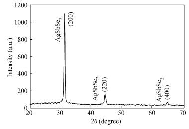
Fig. 1.
X-ray diffraction spectra of a typical silver antimony selenide thin film.
SEMICONDUCTOR PHYSICS
T Namitha Asokan1, , K S Urmila1, Rajani Jacob2, Rachel Reena Philip2, G S Okram3, V Ganesan3 and B Pradeep1
Corresponding author: T Namitha Asokan, Email:namithaasokan@gmail.com
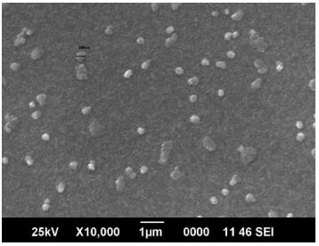
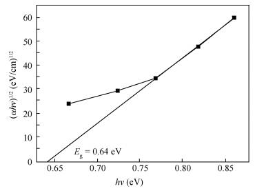
Abstract: Polycrystalline thin films of silver antimony selenide have been deposited using a reactive evaporation technique onto an ultrasonically cleaned glass substrate at a vacuum of 10-5 torr. The preparative parameters, like substrate temperature and incident fluxes, have been properly controlled in order to get stoichiometric, good quality and reproducible thin film samples. The samples are characterized by XRD, SEM, AFM and a UV-vis-NIR spectrophotometer. The prepared sample is found to be polycrystalline in nature. From the XRD pattern, the average particle size and lattice constant are calculated. The dislocation density, strain and number of crystallites per unit area are evaluated using the average particle size. The dependence of the electrical conductivity on the temperature has also been studied and the prepared AgSbSe2 samples are semiconducting in nature. The AgSbSe2 thin films exhibited an indirect allowed optical transition with a band gap of 0.64 eV. The compound exhibits promising thermoelectric properties, a large Seebeck coefficient of 30 mV/K at 48 K due to strong phonon electron interaction. It shows a strong temperature dependence on thermoelectric properties, including the inversion of a dominant carrier type from p to n over a low temperature range 9-300 K, which is explained on the basis of a phonon drag effect.
Keywords: silver antimony selenide, reactive evaporation, thermoelectric power, phonon drag effect
| [1] |
Kumar R S, Sekar A, Jaya N V, et al. Synthesis and high pressure studies of the semiconductor AgSbSe2. Journal of Alloys and Compounds, 1999, 285:48 doi: 10.1016/S0925-8388(99)00018-3
|
| [2] |
Soliman, Abdel-Hady D, Ibrahim E. Optical properties of thermally vacuum evaporated AgSbSe2 thin films. J Condens Matter, 1998, 10:847 doi: 10.1088/0953-8984/10/4/013
|
| [3] |
Patel A R, Lakshminarayana D. Effect of substrate temperature on the crystalliniy of AgSbSe2 films. Thin Solid Films, 1982, 98:59 doi: 10.1016/0040-6090(82)90627-7
|
| [4] |
El-Zahed H. Electrical and structural studies of AgSbSe2 thin films. Thin Sold Films, 1994, 238:104 doi: 10.1016/0040-6090(94)90657-2
|
| [5] |
Hamam M, El-Gendy Y, Selim M S, et al. Optical properties of thermally evaporated AgSbSe2 thin films. Journal of Applied Sciences Research, 2009, 5:2323
|
| [6] |
Garza J G, Shaji S, Arato A M, et al. Chemically deposited silver antimony selenide thin films for photovoltaic applications. Mater Res Soc Symp Proc, 2009, 1165:M08
|
| [7] |
Abdelghany A, Elsayed S N, Abdelwahab D M, et al. Electrical conductivity and thermoelectric power of AgSbSe2 in the solid and liquid states. Mater Chem Phys, 1996, 44:277 doi: 10.1016/0254-0584(96)80069-1
|
| [8] |
Bindu K, Campos J, Nair M T S, et al. Semiconducting AgSbSe2 thin film and its application in a photovoltaic structure. Semicond Sci Technol, 2005, 20:496 doi: 10.1088/0268-1242/20/6/004
|
| [9] |
Wojciechowski K, Tobola J, Schmidt M, et al. Crystal structure, electronic and transport properties of AgSbSe2 and AgSbTe2. J Phys Chem Solids, 2010, 69:2748
|
| [10] |
Schmidt M, Zybala R, Wojciechowski K T. Structural and thermoelectric properties of AgSbSe2-AgSbTe2 system. Materialy Ceramiczne/Ceramic Materials, 2010, 62:465
|
| [11] |
Günther K G. The use of thin films in physical investigation. Anderson J C, ed. London: Academic Press, 1996: 213
|
| [12] |
Soni A, Okram G S. Resistivity and thermopower measurement setups in the temperature range of 5-325 K. Rev Sci Instrum, 2008, 79:125103 doi: 10.1063/1.3048545
|
| [13] |
Powder Diffraction file. Joint Committee on Powder Diffraction Standards (JCPDS) (SwarthmorePA), ASTM card no. 12-379. 1948
|
| [14] |
Cullity B D. Elements of X-ray diffraction. USA:Addison-Wesley Publishing Company Inc, 1956:102
|
| [15] |
Dhanam M, Manoj P K, Prabhu R R. High-temperature conductivity in chemical bath deposited copper selenide thin films. J Crystal Growth, 2005, 280:425 doi: 10.1016/j.jcrysgro.2005.01.111
|
| [16] |
Patel A R, Lakshminarayana D, Rao K V. Growth and crystallization of AgSbSe2 films. Thin Solid Films, 1982, 94:51 doi: 10.1016/0040-6090(82)90029-3
|
| [17] |
Swanepoel R. Determination of the thickness and optical constants of amorphous silicon. J Phys E Sci Instrum, 1983, 16:1214 doi: 10.1088/0022-3735/16/12/023
|
| [18] |
Herring C. Theory of thermoelectric power of semiconductors. Phys Rev, 1954, 96:1163 doi: 10.1103/PhysRev.96.1163
|
| [19] |
Sergey V, Ovsyannikov, Shchennikov V V. Phase transitions investigation in ZnTe by thermoelectric power measurements at high pressure. Solid State Commun, 2004, 132:333 doi: 10.1016/j.ssc.2004.07.062
|
| [20] |
Lakhani A A, Jandl S. Thermoelectric power of TiSe2-xSx mixed crystals at low temperatures. Phys Rev B, 1983, 28:1978 doi: 10.1103/PhysRevB.28.1978
|
| [21] |
Mohanachandra K P, Uchil J. Thermoelectric power of CdS ans CdSe films deposited on vibrating substrates. Thin Solid Films, 1997, 305:124 doi: 10.1016/S0040-6090(97)00188-0
|
| [22] |
Wojciechowski K, Schmidt M, Tobola J, et al. Influence of doping on structural and thermoelectric properties of AgSbSe2. J Electron Mater, 2010, 39:2053 doi: 10.1007/s11664-009-1008-8
|
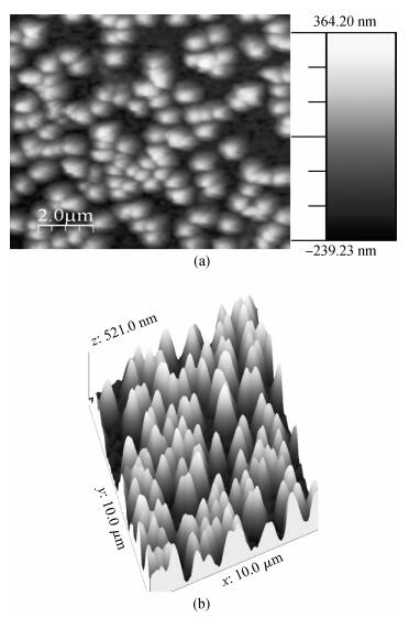
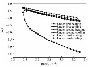
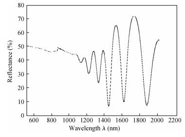
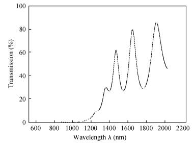

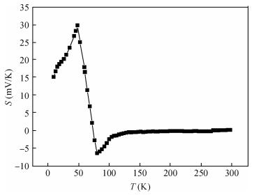
Table 1. The observed XRD data along with standard JCPDS data.

|
| [1] |
Kumar R S, Sekar A, Jaya N V, et al. Synthesis and high pressure studies of the semiconductor AgSbSe2. Journal of Alloys and Compounds, 1999, 285:48 doi: 10.1016/S0925-8388(99)00018-3
|
| [2] |
Soliman, Abdel-Hady D, Ibrahim E. Optical properties of thermally vacuum evaporated AgSbSe2 thin films. J Condens Matter, 1998, 10:847 doi: 10.1088/0953-8984/10/4/013
|
| [3] |
Patel A R, Lakshminarayana D. Effect of substrate temperature on the crystalliniy of AgSbSe2 films. Thin Solid Films, 1982, 98:59 doi: 10.1016/0040-6090(82)90627-7
|
| [4] |
El-Zahed H. Electrical and structural studies of AgSbSe2 thin films. Thin Sold Films, 1994, 238:104 doi: 10.1016/0040-6090(94)90657-2
|
| [5] |
Hamam M, El-Gendy Y, Selim M S, et al. Optical properties of thermally evaporated AgSbSe2 thin films. Journal of Applied Sciences Research, 2009, 5:2323
|
| [6] |
Garza J G, Shaji S, Arato A M, et al. Chemically deposited silver antimony selenide thin films for photovoltaic applications. Mater Res Soc Symp Proc, 2009, 1165:M08
|
| [7] |
Abdelghany A, Elsayed S N, Abdelwahab D M, et al. Electrical conductivity and thermoelectric power of AgSbSe2 in the solid and liquid states. Mater Chem Phys, 1996, 44:277 doi: 10.1016/0254-0584(96)80069-1
|
| [8] |
Bindu K, Campos J, Nair M T S, et al. Semiconducting AgSbSe2 thin film and its application in a photovoltaic structure. Semicond Sci Technol, 2005, 20:496 doi: 10.1088/0268-1242/20/6/004
|
| [9] |
Wojciechowski K, Tobola J, Schmidt M, et al. Crystal structure, electronic and transport properties of AgSbSe2 and AgSbTe2. J Phys Chem Solids, 2010, 69:2748
|
| [10] |
Schmidt M, Zybala R, Wojciechowski K T. Structural and thermoelectric properties of AgSbSe2-AgSbTe2 system. Materialy Ceramiczne/Ceramic Materials, 2010, 62:465
|
| [11] |
Günther K G. The use of thin films in physical investigation. Anderson J C, ed. London: Academic Press, 1996: 213
|
| [12] |
Soni A, Okram G S. Resistivity and thermopower measurement setups in the temperature range of 5-325 K. Rev Sci Instrum, 2008, 79:125103 doi: 10.1063/1.3048545
|
| [13] |
Powder Diffraction file. Joint Committee on Powder Diffraction Standards (JCPDS) (SwarthmorePA), ASTM card no. 12-379. 1948
|
| [14] |
Cullity B D. Elements of X-ray diffraction. USA:Addison-Wesley Publishing Company Inc, 1956:102
|
| [15] |
Dhanam M, Manoj P K, Prabhu R R. High-temperature conductivity in chemical bath deposited copper selenide thin films. J Crystal Growth, 2005, 280:425 doi: 10.1016/j.jcrysgro.2005.01.111
|
| [16] |
Patel A R, Lakshminarayana D, Rao K V. Growth and crystallization of AgSbSe2 films. Thin Solid Films, 1982, 94:51 doi: 10.1016/0040-6090(82)90029-3
|
| [17] |
Swanepoel R. Determination of the thickness and optical constants of amorphous silicon. J Phys E Sci Instrum, 1983, 16:1214 doi: 10.1088/0022-3735/16/12/023
|
| [18] |
Herring C. Theory of thermoelectric power of semiconductors. Phys Rev, 1954, 96:1163 doi: 10.1103/PhysRev.96.1163
|
| [19] |
Sergey V, Ovsyannikov, Shchennikov V V. Phase transitions investigation in ZnTe by thermoelectric power measurements at high pressure. Solid State Commun, 2004, 132:333 doi: 10.1016/j.ssc.2004.07.062
|
| [20] |
Lakhani A A, Jandl S. Thermoelectric power of TiSe2-xSx mixed crystals at low temperatures. Phys Rev B, 1983, 28:1978 doi: 10.1103/PhysRevB.28.1978
|
| [21] |
Mohanachandra K P, Uchil J. Thermoelectric power of CdS ans CdSe films deposited on vibrating substrates. Thin Solid Films, 1997, 305:124 doi: 10.1016/S0040-6090(97)00188-0
|
| [22] |
Wojciechowski K, Schmidt M, Tobola J, et al. Influence of doping on structural and thermoelectric properties of AgSbSe2. J Electron Mater, 2010, 39:2053 doi: 10.1007/s11664-009-1008-8
|


Article views: 2760 Times PDF downloads: 56 Times Cited by: 0 Times
Received: 07 November 2013 Revised: 01 January 2014 Online: Published: 01 May 2014
| Citation: |
T Namitha Asokan, K S Urmila, Rajani Jacob, Rachel Reena Philip, G S Okram, V Ganesan, B Pradeep. Optical and electrical properties and phonon drag effect in low temperature TEP measurements of AgSbSe2 thin films[J]. Journal of Semiconductors, 2014, 35(5): 052001. doi: 10.1088/1674-4926/35/5/052001
****
T N Asokan, K S Urmila, R Jacob, R R Philip, G S Okram, V Ganesan, B Pradeep. Optical and electrical properties and phonon drag effect in low temperature TEP measurements of AgSbSe2 thin films[J]. J. Semicond., 2014, 35(5): 052001. doi: 10.1088/1674-4926/35/5/052001.

|
| [1] |
Kumar R S, Sekar A, Jaya N V, et al. Synthesis and high pressure studies of the semiconductor AgSbSe2. Journal of Alloys and Compounds, 1999, 285:48 doi: 10.1016/S0925-8388(99)00018-3
|
| [2] |
Soliman, Abdel-Hady D, Ibrahim E. Optical properties of thermally vacuum evaporated AgSbSe2 thin films. J Condens Matter, 1998, 10:847 doi: 10.1088/0953-8984/10/4/013
|
| [3] |
Patel A R, Lakshminarayana D. Effect of substrate temperature on the crystalliniy of AgSbSe2 films. Thin Solid Films, 1982, 98:59 doi: 10.1016/0040-6090(82)90627-7
|
| [4] |
El-Zahed H. Electrical and structural studies of AgSbSe2 thin films. Thin Sold Films, 1994, 238:104 doi: 10.1016/0040-6090(94)90657-2
|
| [5] |
Hamam M, El-Gendy Y, Selim M S, et al. Optical properties of thermally evaporated AgSbSe2 thin films. Journal of Applied Sciences Research, 2009, 5:2323
|
| [6] |
Garza J G, Shaji S, Arato A M, et al. Chemically deposited silver antimony selenide thin films for photovoltaic applications. Mater Res Soc Symp Proc, 2009, 1165:M08
|
| [7] |
Abdelghany A, Elsayed S N, Abdelwahab D M, et al. Electrical conductivity and thermoelectric power of AgSbSe2 in the solid and liquid states. Mater Chem Phys, 1996, 44:277 doi: 10.1016/0254-0584(96)80069-1
|
| [8] |
Bindu K, Campos J, Nair M T S, et al. Semiconducting AgSbSe2 thin film and its application in a photovoltaic structure. Semicond Sci Technol, 2005, 20:496 doi: 10.1088/0268-1242/20/6/004
|
| [9] |
Wojciechowski K, Tobola J, Schmidt M, et al. Crystal structure, electronic and transport properties of AgSbSe2 and AgSbTe2. J Phys Chem Solids, 2010, 69:2748
|
| [10] |
Schmidt M, Zybala R, Wojciechowski K T. Structural and thermoelectric properties of AgSbSe2-AgSbTe2 system. Materialy Ceramiczne/Ceramic Materials, 2010, 62:465
|
| [11] |
Günther K G. The use of thin films in physical investigation. Anderson J C, ed. London: Academic Press, 1996: 213
|
| [12] |
Soni A, Okram G S. Resistivity and thermopower measurement setups in the temperature range of 5-325 K. Rev Sci Instrum, 2008, 79:125103 doi: 10.1063/1.3048545
|
| [13] |
Powder Diffraction file. Joint Committee on Powder Diffraction Standards (JCPDS) (SwarthmorePA), ASTM card no. 12-379. 1948
|
| [14] |
Cullity B D. Elements of X-ray diffraction. USA:Addison-Wesley Publishing Company Inc, 1956:102
|
| [15] |
Dhanam M, Manoj P K, Prabhu R R. High-temperature conductivity in chemical bath deposited copper selenide thin films. J Crystal Growth, 2005, 280:425 doi: 10.1016/j.jcrysgro.2005.01.111
|
| [16] |
Patel A R, Lakshminarayana D, Rao K V. Growth and crystallization of AgSbSe2 films. Thin Solid Films, 1982, 94:51 doi: 10.1016/0040-6090(82)90029-3
|
| [17] |
Swanepoel R. Determination of the thickness and optical constants of amorphous silicon. J Phys E Sci Instrum, 1983, 16:1214 doi: 10.1088/0022-3735/16/12/023
|
| [18] |
Herring C. Theory of thermoelectric power of semiconductors. Phys Rev, 1954, 96:1163 doi: 10.1103/PhysRev.96.1163
|
| [19] |
Sergey V, Ovsyannikov, Shchennikov V V. Phase transitions investigation in ZnTe by thermoelectric power measurements at high pressure. Solid State Commun, 2004, 132:333 doi: 10.1016/j.ssc.2004.07.062
|
| [20] |
Lakhani A A, Jandl S. Thermoelectric power of TiSe2-xSx mixed crystals at low temperatures. Phys Rev B, 1983, 28:1978 doi: 10.1103/PhysRevB.28.1978
|
| [21] |
Mohanachandra K P, Uchil J. Thermoelectric power of CdS ans CdSe films deposited on vibrating substrates. Thin Solid Films, 1997, 305:124 doi: 10.1016/S0040-6090(97)00188-0
|
| [22] |
Wojciechowski K, Schmidt M, Tobola J, et al. Influence of doping on structural and thermoelectric properties of AgSbSe2. J Electron Mater, 2010, 39:2053 doi: 10.1007/s11664-009-1008-8
|

 WeChat ID
Journal of Semiconductors © 2017 All Rights Reserved 京ICP备05085259号-2

 DownLoad: