Loading [MathJax]/jax/element/mml/optable/BasicLatin.js
J. Semicond. > 2014, Volume 35 > Issue 6 > 065002

SEMICONDUCTOR INTEGRATED CIRCUITS

A 0.06 mm2 1.0 V 2.5 mW 10 bit 250 MS/s current-steering D/A converter in 65 nm GP CMOS process

Yawei Guo, Li Li, Peng Ou, Zhida Hui, Xu Cheng and Xiaoyang Zeng

+ Author Affiliations

 Corresponding author: Cheng Xu, Email:chengxu@fudan.edu.cn

DOI: 10.1088/1674-4926/35/6/065002

PDF

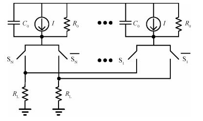
Abstract: A 10 bit 250 MS/s current-steering digital-to-analog converter is presented. Only standard VT core devices are available for the sake of simplicity and low cost. In order to meet the INL performance, a Monte Carlo model is built to analyze the impact of mismatch on integral nonlinearity (INL) yield with both end-point line and best-fit line. A formula is derived for the relationship of INL and output impedance. The relation of dynamic range and output impedance is also discussed. The double centroid layout is adopted for the current source array in order to mitigate the effect of electrical, process, and temperature gradient. An adapted current mirror is used to overcome the gate leakage of the current source array, which cannot be ignored in the 65 nm GP CMOS process. The digital-to-analog converter occupies 0.06 mm2, and consumes 2.5 mW from a single 1.0 V supply at 250 MS/s.

Key words: DACINLDNLSFDR

Much literature has been presented about current-steering digital-to-analog converters (DACs) for wide application including wireless communication. The system-on-chip (SOC) for wireless transceivers needs high performance baseband DAC occupying a small area, consuming very low power, and implemented in nanometer CMOS technology. To achieve good dynamic range with very small area, one technique named random rotation-based binary-weighted selection (RRBS) is proposed in Ref.[1] instead of intrinsic matching of current cell array. It occupies the smallest area of 10-bit current-steering DAC as far as the authors know. However, it compromises the static parameters INL and DNL.

In this work, the design methodology of intrinsic matching DAC is explored to design a very small DAC which meets the static and dynamic performance. In the following sections, a Monte Carlo model is built to analyze the impact of current source mismatch on INL yield. A formula is derived for the relation of INL and output impedance for a differential output current-steering DAC, and the relation of dynamic range and output impedance is analyzed.

Based on those analyses, the proposed 10 bit 250 MS/s current-steering DAC achieves intrinsic 10-bit accuracy and good dynamic performance in the 65 nm GP CMOS process, operating from a single 1.0 V supply, and occupying 0.06 mm2 only. The single 1.0 V supply limits the available overdrive voltage of MOS transistors, thus it becomes difficult to design current-steering DAC in a small area because of the increased impact of VT mismatch. Furthermore, it is hard to achieve high output impedance with nanometer GP CMOS process, especially when the cascode transistors and the switch transistors have minimum length. The gate leakage of core transistors cannot be ignored in the 65 nm GP CMOS process. It even becomes so severe that conventional bias circuitry (current mirror) malfunctions due to the huge total gate area of the current source array. An adapted current mirror is used to overcome the gate leakage in the current source array. The double centroid layout is adopted for the current source array.

The statistic yield model determines the area of unit current source, and eventually determines the area of current-steering DACs. In order to achieve 99.7% yield specification at INL < 1/2 LSB for a 10 bit DAC, the standard deviation of the unity current source must be less than 0.5% based on Bosch's analytical relation[2]. It is derived with the equation

σ(I)I12C2NwithC=inv_norm(0.5+yield2),

(1)

where σ(I)/I is standard deviation of a unity current source, N is the resolution of DAC, inv_norm is inverse cumulative normal distribution function, and yield is relative number of DAC with max INL < 1/2 LSB. However, that is somewhat pessimistic compared to the following Monte Carlo model, which gets more accurate σ(I)/I.

In a Monte Carlo model each unity current source has a Gaussian distributed random value. All the current sources are grouped into thermometer segment and binary segment. INL is calculated with both end-point line and best-fit line. The result of 10, 000 times Monte Carlo simulation is depicted in Fig. 1, where INL yield derived with Bosch's model[2] is plotted for comparison. The Monte Carlo model has more relaxed requirement on σ(I)/I. Furthermore, the INL yield calculated with best-fit line is much better than that calculated with end-point line.

Figure  1.  INL yield versus σ(I)/I.

For 10 bit current-steering DACs, σ(I)/I must be less than 1.25% for 99.7% yield of INL < 0.5 LSB according to the Monte Carlo model of best-fit line INL, and 0.85% according to the Monte Carlo model of end-point line INL as shown in Fig. 1. The gate area of one unity current source is determined by the well-established matching property model of MOS transistor[3],

(WL)min=12[A2β+4A2VT(VGSVT)2]/(σII)2,

(2)

where AVT and Aβ are technology parameters for mismatch, and VGSVT is overdrive voltage. Therefore, for a specific process and overdrive voltage, the gate area of a unity current source predicted with the Monte Carlo model of best-fit line is 16% and 46% only of that predicted with Bosch's model and Monte Carlo model of end-point line, respectively. Thus it is feasible to implement the 10 bit DAC operating from a single 1.0 V supply in very small silicon area.

A simplified current-steering DAC with finite output impedance is shown in Fig. 2. The relationship between the output impedance and static performance is analyzed in Section 3.1; the relationship between the output impedance and dynamic performance is analyzed in Sections 3.2 and 3.3.

Figure  2.  Simplified current-steering DAC.

For the single-ended output the well-known relation for INL and output impedance is[4]

INLRLN24R0,

(3)

where RL is the load resistance, N is the number of unity current source, and R0 is the output resistance of one unity current source. However, Equation (3) is true for a single-ended output current-steering DAC only. The analytical INL model for a differential output current-steering DAC is developed here[5]. The differential output voltage for code k is

V(k)=kIGL+kG0(Nk)IGL+(Nk)G0,

(4)

where GL=1/RL and G0=1/R0. So INL for code k is

INL(k)=V(k)V(0)kV(N)V(0)N.

(5)

Substituting Eq. (4) into Eq. (5) and assuming GLNG0 gives

INL(k)G20k(Nk)(N2k)2GL(GL+NG0).

(6)

Thus INL has maximum value

|INL|max=G202GL(GL+NG0)3N218,

(7)

at k=(6±3)N/6. For a 10 bit differential output DAC with 160 Ω load resistor at each output, the minimum output impedance for one unity current source is 3.6 MΩ with a view to INL less than 0.1 LSB, much smaller than the impedance 2.4 GΩ calculated using Eq. (3). The comparison of INL for differential output and single-ended output is plotted in Fig. 3, assuming the output impedance for one unity current source is 3.6 MΩ, the load is 160 Ω at each output, and the DAC is 10 bit.

Figure  3.  INL of differential output (INLFD) and INL of single-ended output (INLSE).

The relation of output impedance and dynamic range is analyzed for differential output DAC, too[5]. Compared to the static parameters analyzed in the aforementioned part, the dynamic performance is strongly related to the frequency-dependent output impedance of one unity current source. As shown in Fig. 2, the frequency-dependent conductance g0=(1/R0+j2πfC0)/Asw, where Asw is the small signal gain of the switch.

For a sinusoidal output signal, the conductance looking into the positive output is

gout+=Ng01+sin(ωt)2.

(8)

The conductance looking into the negative output is

gout=Ng01sin(ωt)2.

(9)

With the load conductance gL=1/RL, the output voltage at the positive output is

Vout+=NI1+sin(ωt)2gL+Ng0(1+sin(ωt)).

(10)

The output voltage at the negative output is

Vout=NI1sin(ωt)2gL+Ng0(1sin(ωt)).

(11)

The Taylor series expansion of Eq. (10) is

Vout+=a0+a1sin(ωt)+a2sin2(ωt)+a3sin3(ωt)+a4sin4(ωt)+,

(12)

and the Taylor series expansion of Eq. (11) is

Vout=a0a1sin(ωt)+a2sin2(ωt)a3sin3(ωt)+a4sin4(ωt)+,

(13)

where the coefficients are

a0=NI2gL+Ng0,

(14)

a1=(NI2gL+Ng0)22gLNI,

(15)

a2=(NI2gL+Ng0)34g0gLNI2,

(16)

a3=(NI2gL+Ng0)48g20gLNI3,

(17)

a4=(NI2gL+Ng0)416g30gLNI4.

(18)

Thus the differential output signal is

Vout+Vout=2[a1sin(ωt)+a3sin3(ωt)+].

(19)

Obviously Equation (19) is an odd function. Thus the differential output has odd harmonics only. The fundamental is

Fund=2(a1+34a3),

(20)

and the third harmonic is

HD3=12a3.

(21)

Since gL is much greater than g0, the ratio of the 3rd harmonic HD3 and the fundamental signal is approximately[6, 7]

Q32(Ng02gL)2=2(NZL2Z0)2,

(22)

where ZL and Z0 are frequency-dependent output impedance of load and one unity current source, respectively.

Another mechanism called differential capacitive charge transfer was reported in Ref.[8]. A current cell illustrated in Fig. 2 is connected to either positive output or negative output. The total capacitance connected to the positive output is

C+=NC0(1+sin(ωt))2.

(23)

The total capacitance connected to the negative output is

C=NC0(1sin(ωt))2.

(24)

During a cycle, the current cells are switched to positive output from negative output, the voltage on their capacitors C0 varies and causes nonlinear voltage.

Vnl=1gLδQδt=1gL(Vout+Vout)AswδCδt.

(25)

Combine Eq. (23) to Eq. (25), when the positive output is rising

Vnl=2πfN2C0IAswg2Lsin(4πft)4,

(26)

and when the negative output is rising

Vnl=2πfN2C0IAswg2Lsin(4πft)4.

(27)

The 3rd harmonic is

HD3=2πfN2C0IAswg2L45π.

(28)

Based on this mechanism, the ratio of the third harmonic and signal is

Q3=2πfNC0AswgL45π.

(29)

Equation (29) puts more stringent requirement on the output impedance for HD3 than Eq. (22), and it dominates the dynamic performance over most frequency range that we are interested in. In Eq. (29), gL is chosen by the system application. The capacitance C0 is mainly determined by the gate source capacitance of the switch, which is approximately

C0=23CoxWswLsw,

(30)

where Cox is the unity gate capacitance of the switch transistor, Wsw and Lsw are the width and length of the switch transistor, respectively.

The square law model is used to derive the gain of the switch Asw.

Asw=2μCoxWswLswIDSVE,

(31)

where IDS is the drain current of the switch transistor, and VE is the early voltage of the switch transistor.

Substitute Eqs. (30) and (31) into Eq. (29),

Q3=2πf4N5πgL2VE3CoxWswLswIDS2μ.

(32)

It indicates that the switch must be set to minimum channel length in order to improve the dynamic performance, and the width of the switch must be as small as possible, too. Since the square law is used to derive the gain of the switch Asw, it implies that the switch should be kept in saturation region when it is on. This is in accordance with the requirement of Eq. (29).

The DAC is composed of current source array, cascode transistors, switches, thermometer decoder, synchronization latch, and bias circuitry.

The current source array adopts a 6-4 segmented architecture. It has double centroid layout. Q3 rotated walk switching scheme[11] is adopted for each quadrant of the current source array. It mitigates the graded and parabolic errors caused by electrical, process and temperature gradients. Two dummy rows and columns are put along each side to reduce the edge effects. The size of current source is minimized with the aforementioned analysis. It is beneficial to the dynamic range because the drain capacitance of unity current source may affect the output impedance severely at relative low frequency.

The cascode transistors are put outside of the current source array in order to make the current source array compact. The compact layout of the current source array improves the matching of current sources and reduces the graded and parabolic errors. The cascode transistor is put adjacent to the switch in order to minimize the capacitance C0 in Fig. 2, which is critical to the dynamic performance as indicated by Eq. (29).

The complementary outputs of synchronization latch are adjusted for a low crossover point, thus the PMOS switches are not turned off simultaneously[9]. The schematic of the synchronization latch[10] is shown in Fig. 4. Due to the crossover point of node S and node SN being lowered to the threshold of conducting the switch transistor, one switch transistor is turned off immediately after the other switch is turned on when the voltage of nodes S and SN go through that crossover point. This scheme reduces glitch energy because the switches source node is charged when both switches are turned off simultaneously and they introduce glitch when the switches source node is discharged. Of course the clocked MOS transistors are dimensioned to reduce the clock coupling when the data input does not vary. The clock tree to all synchronization switches is balanced to reduce the clock skew.

Figure  4.  Synchronization latch.

The gate leakage cannot be ignored because of the very thin oxide of the 65 nm GP CMOS process[12]. The simulation reveals tens of μA gate leakage and the conventional current mirror cannot sustain suitable bias voltage for current source array, because the gate leakage current is sourced through M3 and M4 if the gate of MCS is tied to the drain of M3 in Fig. 5. An adapted current mirror is used for overcoming the gate leakage current, which is shown in Fig. 5[13]. M1 and M2 are two source followers. The gate leakage of MCS flows in M2. The gate of M2 is driven by M1. In this scheme, the minimum supply is 2VGSP+VDSN. The voltage of the gate of M1 is

Figure  5.  Adapted current mirror.

Vx=VsupVGS,MCSVGS,M2+VGS,M1VsupVGS,MCS.

(33)

Thus it prevents M3 and M4 from operating in triode region, which may occur in a current mirror with a PMOS source follower tied to the gate of MCS from the drain of M3 because the supply is 1.0 V only.

The microphotograph of the DAC core on the test chip is depicted in Fig. 6. The blocks in the DAC are not discernable because it is covered by the power and ground planes using higher metal layers. It occupies 0.06 mm2 silicon areas and consumes 2.5 mW at 250 MS/s sample rate, operating from a single 1.0 V supply.

Figure  6.  Microphotograph of the 10 bit DAC core.

The max INL are all less than 0.4 LSB for all 7 chips measured in the lab, which agrees well with the statistic yield model proposed in Section 2 and the relation for INL and output impedance in Section 3. A typical INL/DNL plot is depicted in Fig. 7, where DNL is 0.19 LSB and INL is 0.25 LSB. One screenshot of the spectrum analyzer for 121 MHz signal at 250 MS/s sampling rate is shown in Fig. 8. The SFDR versus signal frequency is shown in Fig. 9. The measured SFDR at 100 MS/s and 250 MS/s is compared with the expected SFDR with Eq. (29). It is kept above 57 dB over the entire Nyquist band at 250 MS/s sample rate. The SFDR of the 10 MHz signal are kept beyond 70 dB up to 1.25 GS/s as shown in Fig. 10.

Figure  7.  Measured DNL and INL.
Figure  8.  Spectrum of 121 MHz signal at 250 MS/s sample rate.
Figure  9.  SFDR versus signal frequency.
Figure  10.  SFDR @ 10 MHz signal versus clock frequency.

Table 1 summarizes the performance of this work and compares it with other 10 bit DACs and one 14 bit DAC recently published. Two figures of merit (FOM)[14, 8]

Table  1.  Performance summary of the DAC and comparison with other 10 bit DACs.
DownLoad: CSV  | Show Table

{\rm FOM1}=\frac{2^{2N}\times f_{\rm s} @({\rm SFDR}=6(N-1))}{P\times {\rm area}},

(34)

{\rm FOM2}=\frac{2^{\frac{{\rm SFDR}_{\rm DC} }{6.02}}\times 2^{\frac{{\rm SFDR}_{\rm Nyquist} }{6.02}}\times f_{\rm clk} }{P-0.5\times I_{\rm load}^2 \times R_{\rm load}},

(35)

are shown in Eqs. (34) and (35), where N is the resolution, P is the power consumption, area is the DAC core area, f_{\rm s} is the signal frequency where SFDR drops 6 dB compared with the expected result (6N dB), f_{\rm clk} is the clock frequency, SFDR_{\rm DC} is the SFDR at low signal frequency, and SFDR_{\rm Nyquist} is the minimum SFDR over the entire Nyquist band.

A 10 bit current-steering DAC is implemented in the 65 nm GP CMOS process with standard core devices (standard V_{\rm T} 1.0 V transistor) only. It consumes 2.5 mW from a single 1.0 V supply when operating at 250 MS/s sample rate. It occupies 0.06 mm^{2} silicon area, much smaller than most published 10 bit DACs. This work is realized based on extensive statistical analysis of INL yield versus mismatch of unity current source, and analysis of the effect of output impedance on INL and SFDR. An adapted current mirror is adopted for overcoming the gate leakage of the current source array. At last, FOMs are better than other current-steering DACs recently published.

Acknowledgment: The authors would like to thank Wang Biao and Chen Jun for valuable test support.


[1]
Lin W, Kuo T. A compact dynamic-performance-improved current-steering DAC with random rotation-based binary-weighted selection. IEEE J Solid-State Circuits, 2012, 37(2):444 http://ieeexplore.ieee.org/xpl/articleDetails.jsp?reload=true&tp=&arnumber=6059519&contentType=Journals+%26+Magazines&searchField%3DSearch_All%26queryText%3DCurrent+Steering+DAC
[2]
Van den Bosch A, Borremans M A F, Steyaert M S J, et al. A 10-bit 1-GSample/s Nyquist current-steering CMOS D/A converter. IEEE J Solid-State Circuits, 2001, 36(3):315 doi: 10.1109/4.910469
[3]
Pelgrom M J M, Duinmaijer A C J, Welbers A P G. Matching properties of MOS transistors. IEEE J Solid-State Circuits, 1989, 24(5):1433 doi: 10.1109/JSSC.1989.572629
[4]
Razavi B. Principles of data conversion system design. New York:Wiley-IEEE Press, 1994
[5]
Hui Z, Yuan Y, Guo Y, et al. A low-power digital-to-analog converter for GSM wireless transmitters. Research & Progress of SSE, 2011, 31(1):90 http://en.cnki.com.cn/article_en/cjfdtotal-gtdz201101022.htm
[6]
Van den Bosch A, Steyaert M, Sansen W. SFDR-bandwidth limitations for high speed high resolution current steering CMOS D/A converters. Proc IEEE Int Conf Electron, Circuits Syst, 1999:1193 http://ieeexplore.ieee.org/xpl/articleDetails.jsp?arnumber=814383&pageNumber%3D34018%26rowsPerPage%3D100
[7]
Luschas S, Lee H S. Output impedance requirements for DACs. Proc Int Symp Circuits Syst, 2003, 1:I-861 http://ieeexplore.ieee.org/xpl/articleDetails.jsp?arnumber=1205700
[8]
Palmers P, Steyaert M S J. A 10-bit 1.6-GS/s 27-mW current-steering D/A converter with 550-MHz 54-dB SFDR bandwidth in 130-nm CMOS. IEEE Trans Circuits Syst Ⅰ:Reguar Papers, 2010, 57(11):2870 doi: 10.1109/TCSI.2010.2052491
[9]
Bastos J, Marques A M, Steyaert M S J, et al. A 12-bit intrinsic accuracy high-speed CMOS DAC. IEEE J Solid-State Circuits, 1998, 33(12):1959 doi: 10.1109/4.735536
[10]
Deveugele J, Steyaert M S J. A 10-bit 250-MS/s binary-weighted current-steering DAC. IEEE J Solid-State Circuits, 2006, 41(2):320 doi: 10.1109/JSSC.2005.862342
[11]
Lee D, Lin Y, Kuo T. Nyquist-rate current-steering digital-to-analog converters with random multiple data-weighted averaging techinque and QN rotated walk switching scheme. IEEE Trans Circuits Syst Ⅱ:Express Briefs, 2006, 53(11):1264 doi: 10.1109/TCSII.2006.882355
[12]
Gielen G, Dehaene W. Analog and digital circuit design in 65 nm CMOS:end of the road. Proceedings of the Design, Automation and Test in Europe, 2005, 1:37 http://ieeexplore.ieee.org/xpls/icp.jsp?arnumber=1395526
[13]
Seth S, Sreenath S K. Gate leakage insensitive current mirror circuit. US Patent, No. 7332965B2, 2008 http://www.freepatentsonline.com/7332965.html
[14]
Chen T, Geens P, van der Plas G, et al. A 14-bit 130-MHz CMOS current-steering DAC with adjustable INL. Proc IEEE Eur Solid-State Circuits Conf (ESSCIRC), 2004:167 http://ieeexplore.ieee.org/xpl/articleDetails.jsp?reload=true&arnumber=1356644&sortType%3Dasc_p_Sequence%26filter%3DAND%28p_IS_Number%3A29756%29
[15]
Zhao Qi, Li Ran, Qiu Dong, et al. a 14-bit 1-GS/s DAC with a programmable interpolation filter in 65 nm CMOS. Journal of Semiconductors, 2013, 34(2):025004 doi: 10.1088/1674-4926/34/2/025004
Fig. 1.  INL yield versus \sigma (I)/I.

Fig. 2.  Simplified current-steering DAC.

Fig. 3.  INL of differential output (INLFD) and INL of single-ended output (INLSE).

Fig. 4.  Synchronization latch.

Fig. 5.  Adapted current mirror.

Fig. 6.  Microphotograph of the 10 bit DAC core.

Fig. 7.  Measured DNL and INL.

Fig. 8.  Spectrum of 121 MHz signal at 250 MS/s sample rate.

Fig. 9.  SFDR versus signal frequency.

Fig. 10.  SFDR @ 10 MHz signal versus clock frequency.

Table 1.   Performance summary of the DAC and comparison with other 10 bit DACs.

[1]
Lin W, Kuo T. A compact dynamic-performance-improved current-steering DAC with random rotation-based binary-weighted selection. IEEE J Solid-State Circuits, 2012, 37(2):444 http://ieeexplore.ieee.org/xpl/articleDetails.jsp?reload=true&tp=&arnumber=6059519&contentType=Journals+%26+Magazines&searchField%3DSearch_All%26queryText%3DCurrent+Steering+DAC
[2]
Van den Bosch A, Borremans M A F, Steyaert M S J, et al. A 10-bit 1-GSample/s Nyquist current-steering CMOS D/A converter. IEEE J Solid-State Circuits, 2001, 36(3):315 doi: 10.1109/4.910469
[3]
Pelgrom M J M, Duinmaijer A C J, Welbers A P G. Matching properties of MOS transistors. IEEE J Solid-State Circuits, 1989, 24(5):1433 doi: 10.1109/JSSC.1989.572629
[4]
Razavi B. Principles of data conversion system design. New York:Wiley-IEEE Press, 1994
[5]
Hui Z, Yuan Y, Guo Y, et al. A low-power digital-to-analog converter for GSM wireless transmitters. Research & Progress of SSE, 2011, 31(1):90 http://en.cnki.com.cn/article_en/cjfdtotal-gtdz201101022.htm
[6]
Van den Bosch A, Steyaert M, Sansen W. SFDR-bandwidth limitations for high speed high resolution current steering CMOS D/A converters. Proc IEEE Int Conf Electron, Circuits Syst, 1999:1193 http://ieeexplore.ieee.org/xpl/articleDetails.jsp?arnumber=814383&pageNumber%3D34018%26rowsPerPage%3D100
[7]
Luschas S, Lee H S. Output impedance requirements for DACs. Proc Int Symp Circuits Syst, 2003, 1:I-861 http://ieeexplore.ieee.org/xpl/articleDetails.jsp?arnumber=1205700
[8]
Palmers P, Steyaert M S J. A 10-bit 1.6-GS/s 27-mW current-steering D/A converter with 550-MHz 54-dB SFDR bandwidth in 130-nm CMOS. IEEE Trans Circuits Syst Ⅰ:Reguar Papers, 2010, 57(11):2870 doi: 10.1109/TCSI.2010.2052491
[9]
Bastos J, Marques A M, Steyaert M S J, et al. A 12-bit intrinsic accuracy high-speed CMOS DAC. IEEE J Solid-State Circuits, 1998, 33(12):1959 doi: 10.1109/4.735536
[10]
Deveugele J, Steyaert M S J. A 10-bit 250-MS/s binary-weighted current-steering DAC. IEEE J Solid-State Circuits, 2006, 41(2):320 doi: 10.1109/JSSC.2005.862342
[11]
Lee D, Lin Y, Kuo T. Nyquist-rate current-steering digital-to-analog converters with random multiple data-weighted averaging techinque and QN rotated walk switching scheme. IEEE Trans Circuits Syst Ⅱ:Express Briefs, 2006, 53(11):1264 doi: 10.1109/TCSII.2006.882355
[12]
Gielen G, Dehaene W. Analog and digital circuit design in 65 nm CMOS:end of the road. Proceedings of the Design, Automation and Test in Europe, 2005, 1:37 http://ieeexplore.ieee.org/xpls/icp.jsp?arnumber=1395526
[13]
Seth S, Sreenath S K. Gate leakage insensitive current mirror circuit. US Patent, No. 7332965B2, 2008 http://www.freepatentsonline.com/7332965.html
[14]
Chen T, Geens P, van der Plas G, et al. A 14-bit 130-MHz CMOS current-steering DAC with adjustable INL. Proc IEEE Eur Solid-State Circuits Conf (ESSCIRC), 2004:167 http://ieeexplore.ieee.org/xpl/articleDetails.jsp?reload=true&arnumber=1356644&sortType%3Dasc_p_Sequence%26filter%3DAND%28p_IS_Number%3A29756%29
[15]
Zhao Qi, Li Ran, Qiu Dong, et al. a 14-bit 1-GS/s DAC with a programmable interpolation filter in 65 nm CMOS. Journal of Semiconductors, 2013, 34(2):025004 doi: 10.1088/1674-4926/34/2/025004
1

A 10 bit 50 MS/s SAR ADC with partial split capacitor switching scheme in 0.18 μm CMOS

Dong Li, Qiao Meng, Fei Li

Journal of Semiconductors, 2016, 37(1): 015004. doi: 10.1088/1674-4926/37/1/015004

2

A 10 Gsps 8 bit digital-to-analog converter with a built-in self-test circuit

Lei Zhou, Danyu Wu, Fan Jiang, Zhi Jin, Xinyu Liu, et al.

Journal of Semiconductors, 2013, 34(12): 125007. doi: 10.1088/1674-4926/34/12/125007

3

The architecture design of a 2mW 18-bit high speed weight voltage type DAC based on dual weight resistance chain

Qixing Chen, Qiyu Luo

Journal of Semiconductors, 2013, 34(3): 035010. doi: 10.1088/1674-4926/34/3/035010

4

Robust design of a 500-MS/s 10-bit triple-channel current-steering DAC in 40 nm CMOS

Long Cheng, Yu Zhu, Kai Zhu, Chixiao Chen, Junyan Ren, et al.

Journal of Semiconductors, 2013, 34(10): 105007. doi: 10.1088/1674-4926/34/10/105007

5

A 14-bit 1-GS/s DAC with a programmable interpolation filter in 65 nm CMOS

Qi Zhao, Ran Li, Dong Qiu, Ting Yi, Yang Liu Bill, et al.

Journal of Semiconductors, 2013, 34(2): 025004. doi: 10.1088/1674-4926/34/2/025004

6

A low glitch 12-bit current-steering CMOS DAC for CNC systems

Jianming Lei, Hanshu Gui, Beiwen Hu

Journal of Semiconductors, 2013, 34(2): 025007. doi: 10.1088/1674-4926/34/2/025007

7

A 14-bit 250-MS/s current-steering CMOS digital-to-analog converter

Xueqing Li, Hua Fan, Qi Wei, Zhen Xu, Jianan Liu, et al.

Journal of Semiconductors, 2013, 34(8): 085013. doi: 10.1088/1674-4926/34/8/085013

8

A 14-bit 80 MS/s CMOS ADC with 84.8 dB SFDR and 72 dB SNDR

Cai Hua, Li Ping, Cen Yuanjun, Zhu Zhiyong

Journal of Semiconductors, 2012, 33(2): 025012. doi: 10.1088/1674-4926/33/2/025012

9

A 10-bit 80-MS/s opamp-sharing pipelined ADC with a switch-embedded dual-input MDAC

Yin Rui, Liao Youchun, Zhang Wei, Tang Zhangwen

Journal of Semiconductors, 2011, 32(2): 025006. doi: 10.1088/1674-4926/32/2/025006

10

Design and application of a depletion-mode NJFET in a high-voltage BiCMOS process

Liu Yong, Tang Zhaohuan, Wang Zhikuan, Yang Yonghui, Yang Weidong, et al.

Journal of Semiconductors, 2010, 31(8): 084006. doi: 10.1088/1674-4926/31/8/084006

11

A 10-bit 50-MS/s subsampling pipelined ADC based on SMDAC and opamp sharing

Chen Lijie, Zhou Yumei, Wei Baoyue

Journal of Semiconductors, 2010, 31(11): 115006. doi: 10.1088/1674-4926/31/11/115006

12

A 12-bit 40 MS/s pipelined ADC with over 80 dB SFDR

Wei Qi, Yin Xiumei, Han Dandan, Yang Huazhong

Journal of Semiconductors, 2010, 31(2): 025007. doi: 10.1088/1674-4926/31/2/025007

13

An undersampling 14-bit cyclic ADC with over 100-dB SFDR

Li Weitao, Li Fule, Guo Dandan, Zhang Chun, Wang Zhihua, et al.

Journal of Semiconductors, 2010, 31(2): 025008. doi: 10.1088/1674-4926/31/2/025008

14

A current-steering self-calibration 14-bit 100-MSPs DAC

Qiu Dong, Fang Sheng, Li Ran, Xie Renzhong, Yi Ting, et al.

Journal of Semiconductors, 2010, 31(12): 125007. doi: 10.1088/1674-4926/31/12/125007

15

A direct digital frequency synthesizer with high-speed current-steering DAC

Yu Jinshan, Fu Dongbing, Li Ruzhang, Yao Yafeng, Yan Gang, et al.

Journal of Semiconductors, 2009, 30(10): 105006. doi: 10.1088/1674-4926/30/10/105006

16

A high speed direct digital frequency synthesizer realized by a segmented nonlinear DAC

Yuan Ling, Ni Weining, Hao Zhikun, Shi Yin, Li Wenchang, et al.

Journal of Semiconductors, 2009, 30(9): 095003. doi: 10.1088/1674-4926/30/9/095003

17

A 10b 40MS/s, 72dB SFDR Pipelined ADC for DTMB Receivers

Yin Xiumei, Wei Qi, Yang Bin, Yang Huazhong

Journal of Semiconductors, 2008, 29(2): 366-370.

18

A Novel Inline Type Microwave Power Sensor

Han Lei, Huang Qing'an, Liao Xiaoping

Chinese Journal of Semiconductors , 2007, 28(7): 1144-1148.

19

Design of a Novel Video-Rate Adaptive Equalizer IC

Huang Jiaoying, He Yigang, Shen Fang

Chinese Journal of Semiconductors , 2006, 27(8): 1503-1507.

20

一种改进的高速DAC电流开关及其控制信号的产生

Chinese Journal of Semiconductors , 2003, 24(9): 991-993.

  • Search

    Advanced Search >>

    GET CITATION

    Yawei Guo, Li Li, Peng Ou, Zhida Hui, Xu Cheng, Xiaoyang Zeng. A 0.06 mm2 1.0 V 2.5 mW 10 bit 250 MS/s current-steering D/A converter in 65 nm GP CMOS process[J]. Journal of Semiconductors, 2014, 35(6): 065002. doi: 10.1088/1674-4926/35/6/065002
    Y W Guo, L Li, P Ou, Z D Hui, X Cheng, X Y Zeng. A 0.06 mm2 1.0 V 2.5 mW 10 bit 250 MS/s current-steering D/A converter in 65 nm GP CMOS process[J]. J. Semicond., 2014, 35(6): 065002. doi: 10.1088/1674-4926/35/6/065002.
    shu

    Export: BibTex EndNote

    Article Metrics

    Article views: 2658 Times PDF downloads: 27 Times Cited by: 0 Times

    History

    Received: 30 November 2013 Revised: 26 January 2014 Online: Published: 01 June 2014

    Catalog

      Email This Article

      User name:
      Email:*请输入正确邮箱
      Code:*验证码错误
      Yawei Guo, Li Li, Peng Ou, Zhida Hui, Xu Cheng, Xiaoyang Zeng. A 0.06 mm2 1.0 V 2.5 mW 10 bit 250 MS/s current-steering D/A converter in 65 nm GP CMOS process[J]. Journal of Semiconductors, 2014, 35(6): 065002. doi: 10.1088/1674-4926/35/6/065002 ****Y W Guo, L Li, P Ou, Z D Hui, X Cheng, X Y Zeng. A 0.06 mm2 1.0 V 2.5 mW 10 bit 250 MS/s current-steering D/A converter in 65 nm GP CMOS process[J]. J. Semicond., 2014, 35(6): 065002. doi: 10.1088/1674-4926/35/6/065002.
      Citation:
      Yawei Guo, Li Li, Peng Ou, Zhida Hui, Xu Cheng, Xiaoyang Zeng. A 0.06 mm2 1.0 V 2.5 mW 10 bit 250 MS/s current-steering D/A converter in 65 nm GP CMOS process[J]. Journal of Semiconductors, 2014, 35(6): 065002. doi: 10.1088/1674-4926/35/6/065002 ****
      Y W Guo, L Li, P Ou, Z D Hui, X Cheng, X Y Zeng. A 0.06 mm2 1.0 V 2.5 mW 10 bit 250 MS/s current-steering D/A converter in 65 nm GP CMOS process[J]. J. Semicond., 2014, 35(6): 065002. doi: 10.1088/1674-4926/35/6/065002.

      A 0.06 mm2 1.0 V 2.5 mW 10 bit 250 MS/s current-steering D/A converter in 65 nm GP CMOS process

      DOI: 10.1088/1674-4926/35/6/065002
      Funds:

      Project supported by the Doctoral Fund of Ministry of Education of China (No. 20110071110014)

      the Doctoral Fund of Ministry of Education of China 20110071110014

      More Information
      • Corresponding author: Cheng Xu, Email:chengxu@fudan.edu.cn
      • Received Date: 2013-11-30
      • Revised Date: 2014-01-26
      • Published Date: 2014-06-01

      Catalog

        /

        DownLoad:  Full-Size Img  PowerPoint
        Return
        Return