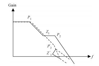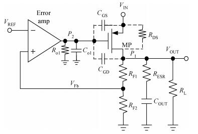
Fig. 1.
Traditional LDO topology.
SEMICONDUCTOR INTEGRATED CIRCUITS
Zhichao Li1, , Yuntao Liu1, Zhangqu Kuang2 and Jie Chen1
Corresponding author: Li Zhichao, Email:lizhichao@ime.ac.cn
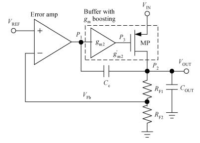
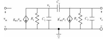
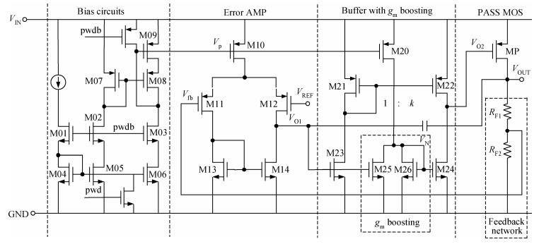
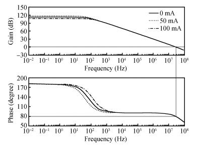
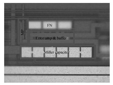
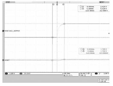
Abstract: This paper presents a capacitor-free CMOS low dropout voltage regulator which has high PSR performance and low chip area. Pole splitting and gm boosting techniques are employed to achieve good stability. The capacitor-free chip LDO was fabricated in commercial 0.18 μm CMOS technology provided by GSMC (Shanghai, China). Measured results show that the capacitor-free LDO has a stable output voltage 1.79 V, when supply voltage changes from 2.5 to 5 V, and the LDO is capable of driving maximum 100 mA load current. The LDO has high power supply rejection about -79 dB at low frequency and -40 dB at 1 MHz frequency, while sacrifice of the LDO's active chip-area is only smaller than 0.02 mm2.
Keywords: CMOS, low dropout regulator, power supply rejection, capacitor-free
| [1] |
Rincon-Mora G A, Allen P E. A low-voltage, low quiescen current, low dropout regulator. IEEE J Solid-State Circuits, 1998, 33(1):36 doi: 10.1109/4.654935
|
| [2] |
Rincon-Mora G A. Active multiplier in Miller-compensated circuits. IEEE J Solid-State Circuits, 2000, 35(1):26 doi: 10.1109/4.818917
|
| [3] |
Leung K N, Mok P K T. A capacitor-free CMOS low dropout regulator with damping factor control frequency compensation. IEEE J Solid-State Circuits, 2003, 38(10):1691 doi: 10.1109/JSSC.2003.817256
|
| [4] |
Gao Leisheng, Zhou Yumei, Wu Bin, et al. A full on-chip CMOS low-dropout voltage regulator with VCCS compensation. Journal of Semiconductors, 2010, 31(8):085006 doi: 10.1088/1674-4926/31/8/085006
|
| [5] |
Milliken R J, Silva-Martinez J, Sanchez-Sinencio E. Full on-chip CMOS low dropout voltage regulator. IEEE Trans Circuits Syst Ⅰ, 2007, 54(9):1879 doi: 10.1109/TCSI.2007.902615
|
| [6] |
Filanovsky I M, Reja M, Ivanov V. Structural design of a CMOS full low dropout voltage regulator. 14th IEEE International Conference on Electronics, Circuits and Systems, 2007:763 http://ieeexplore.ieee.org/xpl/abstractAuthors.jsp?reload=true&arnumber=4511103&contentType=Conference+Publications
|
| [7] |
Zhou Qianneng, Wang Yongsheng, Lai Fengchang. A capacitor-free CMOS LDO regulator with AC-boosting and active-feedback frequency compensation. Journal of Semiconductors, 2009, 30(4):045006 doi: 10.1088/1674-4926/30/4/045006
|
| [8] |
El-Nozahi M, Amer A, Torres J, et al. High PSR low drop-out regulator with feed-forward ripple cancellation technique. IEEE J Solid-State Circuits, 2010, 38(3):565 http://ieeexplore.ieee.org/xpl/articleDetails.jsp?reload=true&tp=&arnumber=5419190&queryText%3DHigh+PSR+Low+Drop-Out+Regulator+With+Feed-Forward+Ripple+Cancellation+Technique
|
| [9] |
Wong K, Evans D. A 150 mA low noise, high PSRR low-dropout linear regulator in 0.13μm technology for RF SoC applications. Proc Eur Solid-State Circuits Conf (ESSCIRC), 2006:532 http://ieeexplore.ieee.org/xpls/icp.jsp?arnumber=4099821
|
| [10] |
Lam Y, Ki W. A 0.9 V 0.35μm adaptively biased CMOS LDO regulator with fast transient response. IEEE Int Solid-State Circuits Conf (ISSCC), 2008:442 http://ieeexplore.ieee.org/xpls/abs_all.jsp?arnumber=4523247
|
| [11] |
Razavi B. Design of analog CMOS integrated circuits. Xi'an Jiaotong University Press, 2002:298
|
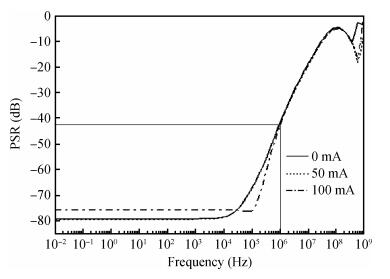

Table 1. Performance of the proposed LDO.

|
| [1] |
Rincon-Mora G A, Allen P E. A low-voltage, low quiescen current, low dropout regulator. IEEE J Solid-State Circuits, 1998, 33(1):36 doi: 10.1109/4.654935
|
| [2] |
Rincon-Mora G A. Active multiplier in Miller-compensated circuits. IEEE J Solid-State Circuits, 2000, 35(1):26 doi: 10.1109/4.818917
|
| [3] |
Leung K N, Mok P K T. A capacitor-free CMOS low dropout regulator with damping factor control frequency compensation. IEEE J Solid-State Circuits, 2003, 38(10):1691 doi: 10.1109/JSSC.2003.817256
|
| [4] |
Gao Leisheng, Zhou Yumei, Wu Bin, et al. A full on-chip CMOS low-dropout voltage regulator with VCCS compensation. Journal of Semiconductors, 2010, 31(8):085006 doi: 10.1088/1674-4926/31/8/085006
|
| [5] |
Milliken R J, Silva-Martinez J, Sanchez-Sinencio E. Full on-chip CMOS low dropout voltage regulator. IEEE Trans Circuits Syst Ⅰ, 2007, 54(9):1879 doi: 10.1109/TCSI.2007.902615
|
| [6] |
Filanovsky I M, Reja M, Ivanov V. Structural design of a CMOS full low dropout voltage regulator. 14th IEEE International Conference on Electronics, Circuits and Systems, 2007:763 http://ieeexplore.ieee.org/xpl/abstractAuthors.jsp?reload=true&arnumber=4511103&contentType=Conference+Publications
|
| [7] |
Zhou Qianneng, Wang Yongsheng, Lai Fengchang. A capacitor-free CMOS LDO regulator with AC-boosting and active-feedback frequency compensation. Journal of Semiconductors, 2009, 30(4):045006 doi: 10.1088/1674-4926/30/4/045006
|
| [8] |
El-Nozahi M, Amer A, Torres J, et al. High PSR low drop-out regulator with feed-forward ripple cancellation technique. IEEE J Solid-State Circuits, 2010, 38(3):565 http://ieeexplore.ieee.org/xpl/articleDetails.jsp?reload=true&tp=&arnumber=5419190&queryText%3DHigh+PSR+Low+Drop-Out+Regulator+With+Feed-Forward+Ripple+Cancellation+Technique
|
| [9] |
Wong K, Evans D. A 150 mA low noise, high PSRR low-dropout linear regulator in 0.13μm technology for RF SoC applications. Proc Eur Solid-State Circuits Conf (ESSCIRC), 2006:532 http://ieeexplore.ieee.org/xpls/icp.jsp?arnumber=4099821
|
| [10] |
Lam Y, Ki W. A 0.9 V 0.35μm adaptively biased CMOS LDO regulator with fast transient response. IEEE Int Solid-State Circuits Conf (ISSCC), 2008:442 http://ieeexplore.ieee.org/xpls/abs_all.jsp?arnumber=4523247
|
| [11] |
Razavi B. Design of analog CMOS integrated circuits. Xi'an Jiaotong University Press, 2002:298
|


Article views: 4403 Times PDF downloads: 194 Times Cited by: 0 Times
Received: 07 November 2013 Revised: 13 January 2014 Online: Published: 01 June 2014
| Citation: |
Zhichao Li, Yuntao Liu, Zhangqu Kuang, Jie Chen. A capacitor-free high PSR CMOS low dropout voltage regulator[J]. Journal of Semiconductors, 2014, 35(6): 065004. doi: 10.1088/1674-4926/35/6/065004
****
Z C Li, Y T Liu, Z Q Kuang, J Chen. A capacitor-free high PSR CMOS low dropout voltage regulator[J]. J. Semicond., 2014, 35(6): 065004. doi: 10.1088/1674-4926/35/6/065004.

|
| [1] |
Rincon-Mora G A, Allen P E. A low-voltage, low quiescen current, low dropout regulator. IEEE J Solid-State Circuits, 1998, 33(1):36 doi: 10.1109/4.654935
|
| [2] |
Rincon-Mora G A. Active multiplier in Miller-compensated circuits. IEEE J Solid-State Circuits, 2000, 35(1):26 doi: 10.1109/4.818917
|
| [3] |
Leung K N, Mok P K T. A capacitor-free CMOS low dropout regulator with damping factor control frequency compensation. IEEE J Solid-State Circuits, 2003, 38(10):1691 doi: 10.1109/JSSC.2003.817256
|
| [4] |
Gao Leisheng, Zhou Yumei, Wu Bin, et al. A full on-chip CMOS low-dropout voltage regulator with VCCS compensation. Journal of Semiconductors, 2010, 31(8):085006 doi: 10.1088/1674-4926/31/8/085006
|
| [5] |
Milliken R J, Silva-Martinez J, Sanchez-Sinencio E. Full on-chip CMOS low dropout voltage regulator. IEEE Trans Circuits Syst Ⅰ, 2007, 54(9):1879 doi: 10.1109/TCSI.2007.902615
|
| [6] |
Filanovsky I M, Reja M, Ivanov V. Structural design of a CMOS full low dropout voltage regulator. 14th IEEE International Conference on Electronics, Circuits and Systems, 2007:763 http://ieeexplore.ieee.org/xpl/abstractAuthors.jsp?reload=true&arnumber=4511103&contentType=Conference+Publications
|
| [7] |
Zhou Qianneng, Wang Yongsheng, Lai Fengchang. A capacitor-free CMOS LDO regulator with AC-boosting and active-feedback frequency compensation. Journal of Semiconductors, 2009, 30(4):045006 doi: 10.1088/1674-4926/30/4/045006
|
| [8] |
El-Nozahi M, Amer A, Torres J, et al. High PSR low drop-out regulator with feed-forward ripple cancellation technique. IEEE J Solid-State Circuits, 2010, 38(3):565 http://ieeexplore.ieee.org/xpl/articleDetails.jsp?reload=true&tp=&arnumber=5419190&queryText%3DHigh+PSR+Low+Drop-Out+Regulator+With+Feed-Forward+Ripple+Cancellation+Technique
|
| [9] |
Wong K, Evans D. A 150 mA low noise, high PSRR low-dropout linear regulator in 0.13μm technology for RF SoC applications. Proc Eur Solid-State Circuits Conf (ESSCIRC), 2006:532 http://ieeexplore.ieee.org/xpls/icp.jsp?arnumber=4099821
|
| [10] |
Lam Y, Ki W. A 0.9 V 0.35μm adaptively biased CMOS LDO regulator with fast transient response. IEEE Int Solid-State Circuits Conf (ISSCC), 2008:442 http://ieeexplore.ieee.org/xpls/abs_all.jsp?arnumber=4523247
|
| [11] |
Razavi B. Design of analog CMOS integrated circuits. Xi'an Jiaotong University Press, 2002:298
|

 WeChat ID
Journal of Semiconductors © 2017 All Rights Reserved 京ICP备05085259号-2

 DownLoad: