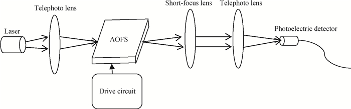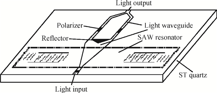
Fig. 1.
Schematic diagram of SAW Raman AOFS.
SEMICONDUCTOR DEVICES
Chunmei Wang1, 2, 3, , Zhiyu Wen1, 2, 3, Zuwei Zhang1, 2, 3 and Yingyi Zhang1, 2, 3
Corresponding author: Wang Chunmei, Email:wangchunmei78@163.com
Abstract: A Raman acousto-optic frequency shifter (AOFS) based on surface acoustic wave (SAW) is presented. It consists of a double-ended SAW resonator and optical waveguide system. The structure parameters of the SAW resonator are optimized using COM software and the optical waveguide system is designed using an effective index method. The AOFS prototype fabricated using MEMS technology is detected. The optical beat signals superimposed by ±1st-order and ±2nd-order diffracted beams are detected. The frequency shift of 78.2201 MHz related to the 1st-order diffracted beams and 156.2306 MHz related to the 2nd-order diffracted beams are obtained respectively.
Keywords: SAW, Raman, AOFS, frequency shift
| [1] |
Zhang N. Theory and technique research of ZnO surface acoustic wave and silicon-based SiO2 optical wave-guide acoustic-optical frequency shifter. Changchun: Changchun University of Technology, 2009
|
| [2] |
Greenhalgh P A, Foord A P, Davies P A. All fiber frequency shifter using piezoceramic SAW device. Electron Lett, 1989, 25(18):1206 doi: 10.1049/el:19890809
|
| [3] |
Wang T Z H. Based on the silicon-based wave-guide and acousto-optic frequency shifter that the research of the theory and technology. Changchun: Changchun University of Technology, 2010
|
| [4] |
Chen S T, Cheng Z Y. Baseband integrated acousto-optic frequency shifter/modulator module for fiber optic at 1.3μm. IEEE Trans Ultrasonics, Ferroelectrics, and Frequency Control, 1993, 40(4):407 doi: 10.1109/58.251290
|
| [5] |
Cheng Z Y, Chen S T. A novel integrated acousto-optic frequency shifter. J Lightwave Technol, 1989, 7(10):1575 doi: 10.1109/50.39100
|
| [6] |
Kakio S, Kitamura M, Nakagawa Y. Waveguide-type acousto-optic frequency shifter with high diffraction efficiency driven by surface acoustic waves and its application to frequency shifted feedback fiber laser. Ultrasonics Symposium, 2003 http://ieeexplore.ieee.org/xpls/abs_all.jsp?arnumber=1418295
|
| [7] |
Kakio S, Uotani S, Nakagawa Y. Waveguide-type acousto-optic frequency shifter with high diffraction efficiency driven by surface acoustic waves. Joint 50th Anniversary Conference International Ultrasonics, Ferroelectrics, and Frequency Control, 2004 http://ieeexplore.ieee.org/xpls/abs_all.jsp?arnumber=1418295
|
| [8] |
Kakio S, Uotani S, Nakagawa Y. Monolithically integrated tandem waveguide-type acousto-optic frequency shifter driven by surface acoustic waves. IEEE Ultrasonics Symposium, 2006 http://ieeexplore.ieee.org/xpls/icp.jsp?arnumber=4151929
|
| [9] |
Liu H X, Gai L, Liu G J. The principle of acousto-optic diffraction and experimental research. Laboratory Research and Exploration, 2009, 28(1):56 http://en.cnki.com.cn/article_en/cjfdtotal-sysy200901021.htm
|
| [10] |
Zhang Y J. Theoretical and experimental research on the photo-electronic integrated acceleration seismic geophone. Tianjin: Tianjin University, 2006
|
| [11] |
Wu Y Q, Shankar P P M. A fiber optic ultrasonic sensor using Raman-Nath light diffraction. Ferroelectrics and Frequency Control, 1994, 41(2):166 doi: 10.1109/58.279129
|
| [12] |
Tang T T, Wang Z H. Integrated optics. Beijing:Science and Technology Press, 2005:51
|
| [13] |
Hashimoto K Y. Surface acoustic wave devices in telecommunication modeling and simulation. Beijing:National Defense Industry Press, 2002:232
|
| [14] |
Zhang H F, Hu G H. Experimental investigation of acousto-optic effect. Journal of Shandong University of Technology, 2008, 22(1):52 http://en.cnki.com.cn/Article_en/CJFDTOTAL-SDGC200801016.htm
|
| [15] |
Fang J X, Cao Z H Q, Yang F Z. The light wave-guide physical basis. Shanghai:Shanghai Jiao Tong University Press, 1987:51
|
| [16] |
Suematsu Y, Hakuta M, Furuya K, et al. Fundamental transverse electric field (TE0) mode selection for thin-film asymmetry light guides. Appl Phys Lett, 1972, 21:291 doi: 10.1063/1.1654383
|
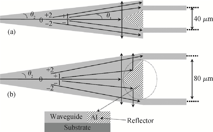
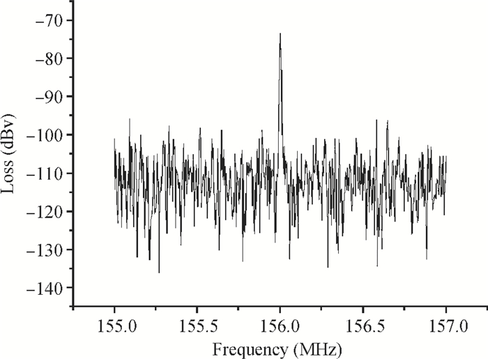
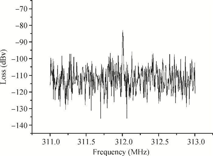
Table 1. Parameters designed of the SAW resonator.

|
Table 2. Performance parameters of the SAW AOFS.

|
| [1] |
Zhang N. Theory and technique research of ZnO surface acoustic wave and silicon-based SiO2 optical wave-guide acoustic-optical frequency shifter. Changchun: Changchun University of Technology, 2009
|
| [2] |
Greenhalgh P A, Foord A P, Davies P A. All fiber frequency shifter using piezoceramic SAW device. Electron Lett, 1989, 25(18):1206 doi: 10.1049/el:19890809
|
| [3] |
Wang T Z H. Based on the silicon-based wave-guide and acousto-optic frequency shifter that the research of the theory and technology. Changchun: Changchun University of Technology, 2010
|
| [4] |
Chen S T, Cheng Z Y. Baseband integrated acousto-optic frequency shifter/modulator module for fiber optic at 1.3μm. IEEE Trans Ultrasonics, Ferroelectrics, and Frequency Control, 1993, 40(4):407 doi: 10.1109/58.251290
|
| [5] |
Cheng Z Y, Chen S T. A novel integrated acousto-optic frequency shifter. J Lightwave Technol, 1989, 7(10):1575 doi: 10.1109/50.39100
|
| [6] |
Kakio S, Kitamura M, Nakagawa Y. Waveguide-type acousto-optic frequency shifter with high diffraction efficiency driven by surface acoustic waves and its application to frequency shifted feedback fiber laser. Ultrasonics Symposium, 2003 http://ieeexplore.ieee.org/xpls/abs_all.jsp?arnumber=1418295
|
| [7] |
Kakio S, Uotani S, Nakagawa Y. Waveguide-type acousto-optic frequency shifter with high diffraction efficiency driven by surface acoustic waves. Joint 50th Anniversary Conference International Ultrasonics, Ferroelectrics, and Frequency Control, 2004 http://ieeexplore.ieee.org/xpls/abs_all.jsp?arnumber=1418295
|
| [8] |
Kakio S, Uotani S, Nakagawa Y. Monolithically integrated tandem waveguide-type acousto-optic frequency shifter driven by surface acoustic waves. IEEE Ultrasonics Symposium, 2006 http://ieeexplore.ieee.org/xpls/icp.jsp?arnumber=4151929
|
| [9] |
Liu H X, Gai L, Liu G J. The principle of acousto-optic diffraction and experimental research. Laboratory Research and Exploration, 2009, 28(1):56 http://en.cnki.com.cn/article_en/cjfdtotal-sysy200901021.htm
|
| [10] |
Zhang Y J. Theoretical and experimental research on the photo-electronic integrated acceleration seismic geophone. Tianjin: Tianjin University, 2006
|
| [11] |
Wu Y Q, Shankar P P M. A fiber optic ultrasonic sensor using Raman-Nath light diffraction. Ferroelectrics and Frequency Control, 1994, 41(2):166 doi: 10.1109/58.279129
|
| [12] |
Tang T T, Wang Z H. Integrated optics. Beijing:Science and Technology Press, 2005:51
|
| [13] |
Hashimoto K Y. Surface acoustic wave devices in telecommunication modeling and simulation. Beijing:National Defense Industry Press, 2002:232
|
| [14] |
Zhang H F, Hu G H. Experimental investigation of acousto-optic effect. Journal of Shandong University of Technology, 2008, 22(1):52 http://en.cnki.com.cn/Article_en/CJFDTOTAL-SDGC200801016.htm
|
| [15] |
Fang J X, Cao Z H Q, Yang F Z. The light wave-guide physical basis. Shanghai:Shanghai Jiao Tong University Press, 1987:51
|
| [16] |
Suematsu Y, Hakuta M, Furuya K, et al. Fundamental transverse electric field (TE0) mode selection for thin-film asymmetry light guides. Appl Phys Lett, 1972, 21:291 doi: 10.1063/1.1654383
|


Article views: 2776 Times PDF downloads: 20 Times Cited by: 0 Times
Received: 16 October 2013 Revised: 04 March 2014 Online: Published: 01 August 2014
| Citation: |
Chunmei Wang, Zhiyu Wen, Zuwei Zhang, Yingyi Zhang. Development of Raman acousto-optic frequency shifter based on SAW[J]. Journal of Semiconductors, 2014, 35(8): 084009. doi: 10.1088/1674-4926/35/8/084009
****
C M Wang, Z Y Wen, Z W Zhang, Y Y Zhang. Development of Raman acousto-optic frequency shifter based on SAW[J]. J. Semicond., 2014, 35(8): 084009. doi: 10.1088/1674-4926/35/8/084009.

|
| [1] |
Zhang N. Theory and technique research of ZnO surface acoustic wave and silicon-based SiO2 optical wave-guide acoustic-optical frequency shifter. Changchun: Changchun University of Technology, 2009
|
| [2] |
Greenhalgh P A, Foord A P, Davies P A. All fiber frequency shifter using piezoceramic SAW device. Electron Lett, 1989, 25(18):1206 doi: 10.1049/el:19890809
|
| [3] |
Wang T Z H. Based on the silicon-based wave-guide and acousto-optic frequency shifter that the research of the theory and technology. Changchun: Changchun University of Technology, 2010
|
| [4] |
Chen S T, Cheng Z Y. Baseband integrated acousto-optic frequency shifter/modulator module for fiber optic at 1.3μm. IEEE Trans Ultrasonics, Ferroelectrics, and Frequency Control, 1993, 40(4):407 doi: 10.1109/58.251290
|
| [5] |
Cheng Z Y, Chen S T. A novel integrated acousto-optic frequency shifter. J Lightwave Technol, 1989, 7(10):1575 doi: 10.1109/50.39100
|
| [6] |
Kakio S, Kitamura M, Nakagawa Y. Waveguide-type acousto-optic frequency shifter with high diffraction efficiency driven by surface acoustic waves and its application to frequency shifted feedback fiber laser. Ultrasonics Symposium, 2003 http://ieeexplore.ieee.org/xpls/abs_all.jsp?arnumber=1418295
|
| [7] |
Kakio S, Uotani S, Nakagawa Y. Waveguide-type acousto-optic frequency shifter with high diffraction efficiency driven by surface acoustic waves. Joint 50th Anniversary Conference International Ultrasonics, Ferroelectrics, and Frequency Control, 2004 http://ieeexplore.ieee.org/xpls/abs_all.jsp?arnumber=1418295
|
| [8] |
Kakio S, Uotani S, Nakagawa Y. Monolithically integrated tandem waveguide-type acousto-optic frequency shifter driven by surface acoustic waves. IEEE Ultrasonics Symposium, 2006 http://ieeexplore.ieee.org/xpls/icp.jsp?arnumber=4151929
|
| [9] |
Liu H X, Gai L, Liu G J. The principle of acousto-optic diffraction and experimental research. Laboratory Research and Exploration, 2009, 28(1):56 http://en.cnki.com.cn/article_en/cjfdtotal-sysy200901021.htm
|
| [10] |
Zhang Y J. Theoretical and experimental research on the photo-electronic integrated acceleration seismic geophone. Tianjin: Tianjin University, 2006
|
| [11] |
Wu Y Q, Shankar P P M. A fiber optic ultrasonic sensor using Raman-Nath light diffraction. Ferroelectrics and Frequency Control, 1994, 41(2):166 doi: 10.1109/58.279129
|
| [12] |
Tang T T, Wang Z H. Integrated optics. Beijing:Science and Technology Press, 2005:51
|
| [13] |
Hashimoto K Y. Surface acoustic wave devices in telecommunication modeling and simulation. Beijing:National Defense Industry Press, 2002:232
|
| [14] |
Zhang H F, Hu G H. Experimental investigation of acousto-optic effect. Journal of Shandong University of Technology, 2008, 22(1):52 http://en.cnki.com.cn/Article_en/CJFDTOTAL-SDGC200801016.htm
|
| [15] |
Fang J X, Cao Z H Q, Yang F Z. The light wave-guide physical basis. Shanghai:Shanghai Jiao Tong University Press, 1987:51
|
| [16] |
Suematsu Y, Hakuta M, Furuya K, et al. Fundamental transverse electric field (TE0) mode selection for thin-film asymmetry light guides. Appl Phys Lett, 1972, 21:291 doi: 10.1063/1.1654383
|

 WeChat ID
Journal of Semiconductors © 2017 All Rights Reserved 京ICP备05085259号-2

 DownLoad: