J. Semicond. > 2014, Volume 35 > Issue 9 > 096003

SEMICONDUCTOR TECHNOLOGY

Effect of novel alkaline copper slurry on 300 mm copper global planarization

Weijuan Liu, Yuling Liu, Chenwei Wang, Guodong Chen, Mengting Jiang, Haobo Yuan and Pengfei Cheng

+ Author Affiliations

 Corresponding author: Liu Weijuan, Email:269227849@qq.com

DOI: 10.1088/1674-4926/35/9/096003

PDF

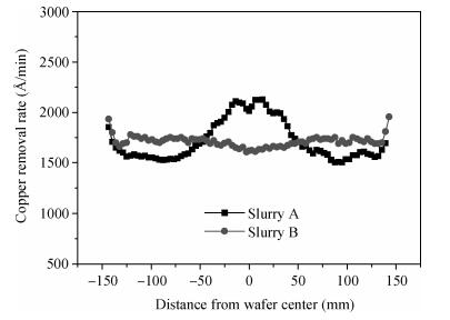
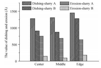
Abstract: The copper removal rate and uniformity of two types copper slurries were investigated, which was performed on the 300 mm chemical mechanical planarization (CMP) platform. The experiment results illustrate that the removal rate of the two slurries is nearly the same. Slurry A is mainly composed of a FA/OⅡ type chelating agent and the uniformity reaches to 88.32%. While the uniformity of slurry B is 96.68%, which is mainly composed of a FA/OV type chelating agent. This phenomenon demonstrates that under the same process conditions, the uniformity of different slurries is vastly different. The CMP performance was evaluated in terms of the dishing and erosion values. In this paper, the relationship between the uniformity and the planarization was deeply analyzed, which is mainly based on the endpoint detection mechanism. The experiment results reveal that the slurry with good uniformity has low dishing and erosion. The slurry with bad uniformity, by contract, increases Cu dishing significantly and causes copper loss in the recessed region. Therefore, the following conclusions are drawn:slurry B can improve the wafer leveling efficiently and minimize the resistance and current density along the line, which is helpful to improve the device yield and product reliability. This investigation provides a guide to improve the uniformity and achieve the global and local planarization. It is very significant to meet the requirements for 22 nm technology nodes and control the dishing and erosion efficiently.

Key words: CMPremoval rateuniformitydishingerosionendpoint detection

Owning the switchable and non-volatile electric polarizations at room temperature, conventional ferroelectrics, such as complex perovskite oxides, have broad applications in electronics, including high energy density capacitor[1], tunable diode[2], ferroelectric tunneling junction (FTJ)[3], and ferroelectric field-effect transistors (FeFET)[4]. With the further miniaturization of electronic devices beyond the Moore’s law, there is a need to explore ferroelectric thin films with nanometer thickness. However, due to the imperfect charge screening, local chemical environment, defects, and misfit strain at the interface, there is depolarization field arising in ultra-thin ferroelectrics, which leads to the so-called critical size effect[59]. The electric polarizations of conventional ferroelectrics will reduce or even disappear when the thickness reaches to the single atomic layer limit. As a consequence, their application in modern electronics is strongly hindered. In parallel, since the rise of graphene, the family of two-dimensional (2D) materials has been greatly expanded with members owning numerous novel physical properties such as superconductivity[10], charge density wave[11], valley polarization[12], and exotic magnetism[13]. These van der Waals (vdW) materials have saturated interface chemical environment, weak interaction between the layers and the benefit of easily preparing stable atomically thin slabs, which offer a novel platform to study some emerging phenomena that have never been observed in their bulk form counterpart. Therefore, it offers a feasible way to explore ferroelectricity at atomic scale in 2D materials, especially for the out-of-plane electric polarizations, which is more important than the in-plane electric polarization from the technological perspective.

In the early days of the research on vdW materials, 2D ferroelectricity is lack of attention with rare findings. The reason is that when the thickness is reduced to nanometer scale, the competition between crystal structure stability and the long-range ordering of electric dipoles will become significant. Thus, for a long time, it is hard to get stable crystal phase with switchable electric polarizations in vdW materials under ambient conditions. As ferroelectrics, the prerequisite is the inversion symmetry breaking in structure. For most of the commonly studied 2D materials, taking graphene as a typical example[14], the centrosymmetric lattice naturally rules out the possibility of being ferroelectric. Even in 2H-MoS2[15, 16], where the inversion symmetry is explicitly broken in its monolayer structure, the presence of the mirror symmetry along its middle plane of metal Mo atoms makes it keeping symmetric Mo-S chemical bonds in the out-of-plane direction, resulting void electric dipoles. Given these facts, seeking 2D ferroelectricity in vdW materials is of challenges but of great values.

The 2D nature of vdW materials allows to explore ferroelectricity in both the in-plane and out-of-plane directions. The in-plane vdW ferroelectrics provide a platform to study domain physics at 2D limit, while the out-of-plane ferroelectric polarizations lay down the fundamental for device applications. In recent years, several candidates of 2D ferroelectrics have been theoretically predicated and verified experimentally. The first example is the layered CuInP2S6. In 2015, Belianinov et al.[17] reported the observation of room-temperature out-of-plane ferroelectricity in bulk CuInP2S6 with film thickness more than 100 nm. The electric polarization stemmed from the off-center ordering of the Cu and In cations in each unit cell with its polar axis along the vertical direction relative to the 2D plane. Although the collinear two-sublattice structure of CuInP2S6 makes it a ferrielectric system, this finding also inspires further exploration on 2D ferroelectrics. Later in 2016, Liu et al.[18] observed the out-of-plane electric polarization in few-layer CuInP2S6 with much thinner thickness of 4 nm under ambient conditions. Utilizing the second harmonic generation (SHG) technique, they clearly showed that the phase transition temperature (Tc) from the ferroelectric phase to the paraelectric phase is 320 K, which is slightly higher than the room temperature. This is crucial for their practical device application. At the same time, Chang et al.[19] from Tsinghua University experimentally reported the first 2D ferroelectric with single atomic layer thickness. They studied the monolayer SnTe with distorted lattice at cryogenic temperature and verified the in-plane ferroelectricity with evidences such as spontaneous domains and electric polarization induced band bending. These pioneering findings open up the route towards 2D ferroelectricity with vdW materials. However, for layered SnTe, the nature as an in-plane ferroelectric strongly hinders its application in practical device application, while for CuInP2S6, it is ferrielectric, resulting relatively weak saturated electric polarizations. From the past researches on ferroelectricity, as a consensus, their practical application relies on the technically more important out-of-plane electric polarization, high Tc and simple lattice structure for material realization. Based on these requirements, very recently Ding et al.[20] predicted the intrinsic room-temperature 2D ferroelectricity with intercorrelated in-plane and out-of-plane electric polarization in the 2D semiconducting α-In2Se3. Stimulated by this unprecedented inter-locking of electric dipoles in α-In2Se3, intense experimental efforts were devoted with various techniques[2128]. Clear ferroelectric domains, ferroelectric hysteresis loop and piezoelectricity have been observed in ultrathin samples with the thickness down to 2D limit[23, 26]. Besides, several practical device applications based on the few layer α-In2Se3 including switchable ferroelectricdiode[24], FeFETs[29], and ferroelectric semiconductor FET (FeS-FET)[30] were demonstrated. These breakthroughs point to the possibility of stable ferroelectric phase in layered vdW materials.

In view of the rapid growing research interest in the 2D ferroelectricity of α-In2Se3, we review some recent relevant progresses in this article. We begin with the introduction of the crystal structure of α-In2Se3 and the corresponding ferroelectricity. The experimental verifications of the in-plane and out-of-plane electric polarizations in ultra-thin α-In2Se3 will be highlighted. Finally, we present two prototypes of ferroelectric devices to demonstrate the potential device application of 2D ferroelectric α-In2Se3.

Layered In2Se3 is an available 2D semiconductor with remarkable optical and electrical properties[3133]. It has long been studied in the application of photo sensors and phase-change memories[3436]. Previous studies have found that the phases of In2Se3 are very rich. In addition to the α phase, there exists crystal structures with different lattice constants, which are labeled as β, γ or δ phase. In all these phases, the α-In2Se3 is recognized as the most stable layered structure at room temperature. As shown in Fig. 1, its single layer is composed of alternating Se or In atomic layer via covalent bonds, constituting a Se–In–Se–In–Se quintuple layer (QL). These QLs are vertically stacked via the weak van der Waals force. However, the identification of the crystal structure for α phase is highly controversial at early stage[3135, 3739], which is due to the small energy barrier in structure stability between the α and β phase.

Figure  1.  (Color online) Layered structures of In2Se3. (a) Three-dimensional crystal structure of layered In2Se3, with the In atoms in blue and Se atoms in red, and a quintuple layer (QL) is indicated by the black dashed square. (b) Top view of the system along the vertical direction. Each atomic layer in a QL contains only one elemental species, with the atoms arranged in one of the triangular lattices A, B or C as illustrated. (c–h) Side views of several representative structures of one QL In2Se3, among which the (c) to (e) structures are derived from the zincblende, wurtzite and fcc crystals, respectively. In (f), the interlayer spacings between the central Se layer and the two neighboring In layers are displayed. The black arrows in (f) and (g) indicate the directions of the spontaneous electric polarization (P) in the FE-ZB' and FE-WZ' structures, respectively. The FE-ZB’ and FE-WZ’ structures in (f) and (g) are identified as α phase, while the metastable structure fcc and fcc’ in (e) and (h) are identified as β phase. (Courtesy of Ref. [20])

To clarify the crystal structure of In2Se3, Ding et al.[20] has performed detailed numerical calculations with density function theory (DFT). They examined the possible atomic arrangements in layered In2Se3, and obtained two lattice structures with lowest total energy in thermodynamics. As shown in Figs. 1(f) and 1(g), the FE-ZB' and the FE-WZ' structures were identified as ground states, which belonged to α phase. From the top view of its crystal structure, there are three positions marked as A, B, and C (represent one corner of the triangular lattices in Fig. 1(b)) that can be occupied by Se or In atoms. Along the out-of-plane direction, the atoms of a given QL in FE-ZB' and FE-WZ' structure are arranged with ABBCA and ABBAC sequence respectively. For the ABCAB structure (Fig. 1(e)), it is identified as β phase, which is metastable at room temperature. With the confirmation of its crystal structure, they predicted the emergence of 2D ferroelectricity in α-In2Se3, which was attributed to the subtle atomic configuration of the central Se atoms. Taking the FE-ZB’ structure as an example, in each QL, the Se and In atoms in the lower three Se–In–Se atomic layers form a regular tetrahedral structure, while the in the upper Se–In–Se layers they form the octahedral structure. Thus, the Se atoms in the middle layer are in different chemical environments with respect to its neighboring layers. This breaks the central inversion symmetry thereby produces the electric polarizations along both the out-of-plane and in-plane direction. Moreover, in α-In2Se3, the in-plane and out-of-plane electric dipoles are inherently coupled, which not only provides a novel approach of electric polarization manipulation with external electric field but also helps the stabilization of the out-of-plane electric polarizations against the depolarization electric field in ultrathin samples. In contrast, the β phase of In2Se3 presented in Fig. 1(e) follows the ABCAB layer sequence with the central inversion symmetry, which forbids the spontaneous formation of net electric polarizations. Meanwhile, due to the structural phase transition, the phonon modes of α and β phases of In2Se3 were predicted to have distinct features, such as the softening of A1 phonon mode in the ferroelectric phase. These Raman modes can be utilized as an effective tool to identify the α-In2Se3 in following experimental studies, including the results in our group[2122, 24, 25, 29].

As for ferroelectrics, one important signature is the switchable electric polarization with external stimulus such as electric field. For α-In2Se3, intuitively, the degenerate polarization states with opposite polarity can be achieved by in-plane 180° rotation of a single QL without changing the crystal structure and symmetry. It has been theoretically suggested that the transformation of these two polarization states is kinetically feasible[20]. The flipping process is proposed as "three-step cooperated polarization inversion process", where the electron polarization reversion is achieved by the metastable fcc' structure (β phase) as the intermediate transition state. The energy barrier for polarization flipping is only 0.066 eV per unit cell, which is comparable with that in conventional ferroelectric material PbTiO3 (0.07 eV/ unit cell). This feasible polarization flipping process in α-In2Se3 further evidence its ferroelectric nature.

Inspired by the previous theoretical prediction, several groups have aimed to experimentally verify the room temperature ferroelectricity in α-phase In2Se3[2126, 28]. Ferroelectrics naturally have the piezoelectric effect, in which deformation of the crystals can be realized by an external electric field. Therefore, the detection of ferroelectricity in vdW materials can be realized via surface sensitive techniques such as Piezo force microscopy (PFM). In most of recent studies on the 2D ferroelectricity in α-In2Se3, PFM was chosen as the versatile tool. Fig. 2 shows the typical PFM study on ultra-thin α-In2Se3 with thickness about 20 nm under ambient condition[24]. The samples were mechanically exfoliated from bulk and post transferred to conductive substrate such as heavily doped Si or Au. Clear out-of-plane spontaneous electric polarizations were visualized through the contrasted PFM phase image as shown in Fig. 2(b). The phase difference between adjacent ferroelectric domains was found to be 180°, indicating that there were antiparallel electric dipoles (Fig. 2(c)) in the out-of-plane direction. In the single poling measurement, the butterfly-like ferroelectric hysteresis is observed in the out-of-plane PFM amplitude (see Fig. 2(d)), and the transition between the two different ferroelectric states can also be driven by an external electric field, with two different critical field strengths during forward and backward sweeping (see Fig. 2(e)). These results show that the electric polarization could be flipped under external electric field. The coercive field (Ec) of α-In2Se3 was found to be about 200 kV/cm[24], which was much lower than that of layered ferroelectric CuInP2S6 (700 kV/cm)[18]. The relatively low Ec benefits the low operating power ferroelectric device based on α-In2Se3. Other important features of ferroelectrics include the domain engineering and the retention of electric polarizations. In order to verify these features, artificially creating the ferroelectric domain structure with the box-in-box pattern (Fig. 2(f)) has been tested in α-In2Se3. In detail, a square area of ​​1 × 1 μm2 is controllably written with positive bias via the PFM tip to establish the downward polarization. After that, the negative sample/tip bias is applied in the center 0.5 × 0.5 μm2 area to reverse or erase the polarization. As a result of the ferroelectric nature of α-In2Se3, an artificial domain structure with the box-in-box pattern is created. It is found that artificial ferroelectric domain could sustain more than 24 h under ambient condition[24].

Figure  2.  (Color online) Ferroelectricity of α-In2Se3 thin layers. (a) The surface topography of α-In2Se3 thin layers (~20 nm) on the heavily doped Si substrate. The scale bar is 2 μm. (b) The corresponding PFM phase image in the out-of-plane direction, showing clear ferroelectric domains. (c) The phase profile of different ferroelectric domains as sketched by the red dashed line in (b). A phase contrast of 180° is observed, which indicates the antiparallel directions of out-of-plane electric polarization between the adjacent domains. The arrows indicate the directions of electric polarization. (d) PFM amplitude and (e) PFM phase hysteresis loop measured from α-In2Se3 thin layers. (f) PFM amplitude image of domain engineering in α-In2Se3 with a film thickness of 12 nm. The scale bar is 370 nm. (Courtesy of Ref. [24])

Another method to study the 2D ferroelectricity in vdW materials is the optical SHG technique, which is a direct probe of the lattice inversion symmetry breaking. With this technique, Xiao et al.[25] has verified the out-of-plane and in-plane electric dipole inter-locking in α-In2Se3, which is consistent with previous PFM study[22]. The rotation of in-plane electric dipole could be achieved by an out-of-plane electric field, which demonstrates the inherent locking of these two orthogonal polarizations. As shown in Fig. 3, in a 3-nm-thick sample with confirmed electric polarization, they first artificially construct the box-in-box domain in the out-of-plane direction with the PFM tip. In their SHG measurements, the normal incidence set-up is chosen, which is only sensitive to the in-plane electric polarization. By comparing the SHG mappings before and after the out-of-plane bias poling (Figs. 3(c) and 3(d)), clear dark lines (less SHG intensity) correspond to the boundaries of the patterned area by PFM tip bias. This observation can be understood as the destructive optical interference arising from the reversal of the in-plane nonlinear optical polarization and corresponding in-plane lattice asymmetry. These findings clearly demonstrate the interlocking of the out-of-plane and in-plane electric dipoles in 2D α-In2Se3. Moreover, the temperature-dependent SHG is also studied, which show that the SHG intensity is robust and is almost independent of temperature in a wide range of temperature range up to 500 K. The transition from the ferroelectric phase to paraelectric phase happens at about 700 K, beyond which a sharp decrease of SHG signal can be found due to the recovery of structural inversion symmetry. These results confirm that the Tc for ferroelectric α-In2Se3 is much higher than that of the other 2D ferroelectrics such as SnTe and CuInP2S6, laying the fundamental basis for its practical device application.

Figure  3.  (Color online) Electrically switching the out-of-plane ferroelectric polarization and corresponding in-plane atomic configuration through dipole locking. (a) The hysteresis of remnant out-of-plane polarization of a 3-nm-thick In2Se3 crystal on conductive SrRuO3, as a function of perpendicular poling voltage. Black, red, blue curves represent the normalized piezoresponse measured with Vac = 0.5, 1, and 1.5 V, respectively. The collapse of the hysteresis loop is similar to the behavior of the conventional field-switchable ferroelectrics, but totally different from charging artifact of dielectrics. (b) Polarized domain patterned by electrically biased scanning probe and measured by PFM. The inner box corresponds to positive applied voltage (+6 V) with positive piezoresponse while the outer box to negative voltage (−6 V) with negative piezoresponse. (c) SHG intensity mapping on another trilayer In2Se3 sample before PFM reversed poling. The area enclosed by dashed line was then scanning by a negatively biased AFM tip. The color bar is in linear scale with arbitrary unit. (d) SHG mapping after the electrical reversed poling. It shows dark lines at the boundary of the patterned area resulting from destructive interference, which indicates the reversal of in-plane crystal orientation and corresponding nonlinear optical polarization after reversed electrical poling. (Courtesy of Ref. [25])

The vacuum potential difference between the top and bottom surfaces of a given α-In2Se3 QL can be as high as 1.4 eV[20]. The sign of this potential difference can be controlled by the direction of polarization. Therefore, when the 2D ferroelectric α-In2Se3 is artificially combined with other vdW materials to form multi-layer vdW heterojunction, the physical properties of the entire heterojunction will be manipulated by the electric polarization. Tuning the properties of the ferroelectric heterojunction as a whole can be simply achieved by reversing the polarity of the ferroelectrics with an external electric field. With this feature, it is convenient to develop multifunctional ferroelectric device with 2D ferroelectrics.

We firstly introduce the ferroelectric diode application based on 2D α-In2Se3. With the out-of-plane ferroelectricity of α-In2Se3, a polarity switchable ferroelectric diode with the vertical few-layer graphene/α-In2Se3/graphene heterojunction is proposed and experimentally demonstrated[24]. Figs. 4(a) and 4(b) show the device structure and optical image of the proposed ferroelectric diode, in which the thickness of the ferroelectric layer α-In2Se3 is as thin as 5 nm. Graphene and few-layer graphene serve as the bottom and top electrodes, respectively. By comparing work functions of α-In2Se3, monolayer graphene (p-type) and few-layer graphene (intrinsic), the Schottky barrier at bottom graphene/α-In2Se3 is found to be higher than α-In2Se3/top graphene. Therefore, the initial state of the diode is in the forward direction, thus the current flows from α-In2Se3 to the FLG. When the device is polarized with +2 V pulse voltage, as shown in Fig. 4(c), it shows an enhanced forward rectifying behavior. However, in the case of –2 V polarized state, the device functions as a backward diode, allowing the current conduction from α-In2Se3 to bottom graphene (Fig. 4(d)). This polarity-controlled rectification effect could be understood through the band structure of the device (Figs. 4(f) and 4(g)). In the α-In2Se3 ferroelectric diode, the polarization reversal in α-In2Se3 changes the direction of the built-in electric field. The Schottky barrier height at the interfaces of the upper and lower sides of α-In2Se3 changes significantly, leading to the switch of the conduction direction of the diode. Further studies on the I–V characteristic of the ferroelectric diode under high DC bias are also performed. The I–V curves are measured by sweeping the bias voltage from –2 to +2 V and then backward to –2 V. As shown in Fig. 4(e), under high DC bias with both positive and negative voltages, the device is at its “on” state due to the modification of Schottky barrier. The on/off ratio of the ferroelectric diode was found to be at the order of ~ 105.

Figure  4.  (Color online) Switchable ferroelectric diode based on α-In2Se3 thin layers. (a) Schematic and (b) optical image of the device. (c) and (d) I–V curves of the ferroelectric diode with switchable rectifying behavior. (e) I–V curves measured under high DC bias, showing clear hysteresis characteristics. The arrows indicate the voltage sweeping sequence. (f) and (g) Schematic of energy band diagrams of the graphene/In2Se3 heterostructure, illustrating the evolution of the Schottky barrier in the polarized state of the ferroelectric. The positive and negative charges on the vertical grey lines stand for the polarization charges on the top and bottom sides of the α-In2Se3 thin layer. The screening charges are visualized in the graphene/FLG electrodes. (Courtesy of Ref. [24])

A second typical example of the ferroelectric device application is the nonvolatile memory via the device so called FeFET, which is a kind of the three-terminal device by separating the reading operation in the conducting channel from the writing operation in and the ferroelectric gate. FeFETs are non-destructive with no requirement on ferroelectric film thickness. However, the thickness of ferroelectric used in conventional FeFET devices are usually of several hundred nanometers due to the constraint of Critical size effect. Therefore, relatively large operation gate voltage is always required. In contrast, 2D ferroelectrics will significantly scale down the dimensions of the device and meanwhile the voltage to flip the electric polarization could be lowered down dramatically, resulting a low-power consumption memory device.

Fig. 5 shows the schematic and optical image of a FeFET device based on graphene and ferroelectric α-In2Se3[29]. Atomically thin hexagonal boron nitride (hBN), monolayer or bilayer, was chosen as the buffer and insulating layer. The introduction of hBN layer not only improvs the device interface properties, such as suppression of ion diffusion and leakage current[40, 41], but also enhances the intrinsic conductivity of graphene by reducing the phonon and Coulomb scatterings. The thinnest thickness of the ferroelectric film in the device is 2.6 nm, which is roughly about the thickness of bilayer α-In2Se3. This thickness is much thinner than conventional ferroelectric layer. The resistance of graphene channel is controllable and retentive due to the electrostatic doping, which stems from the electric polarization of the ferroelectric α-In2Se3. As shown in Fig. 5(b), when sweeping the ferroelectric gate voltage cyclically from negative to positive and back to negative, the resistance of the graphene channel could be efficiently modulated with large and stable hysteresis. By applying the top-gate voltage, the electric dipoles in α-In2Se3 are electrically polarized in the out-of-plane direction, either upward or downward. The dipoles would significantly dope graphene with different types of carriers via the induced screening charges, leading to the change of its Fermi level (EF) accompanied by the resistance modulation of the FeFET device. When the Fermi level is tuned to the Dirac point, the conducting graphene channel reaches its maximum resistance (RMax) state. Two RMax states are found at different top gate voltages in the forward (from negative to positive) and backward (from positive to negative) gate voltage sweeping. The apparent differences of gate voltage at RMax are due to the requirement of coercive electric field for domain reversion in ferroelectric α-In2Se3. However, even under ±5 V gate bias, equivalent to an electrical field strength at the order of 105 V/cm in this device, the ferroelectric polarization in the top α-In2Se3 thin layers does not get saturated. Moreover, it is necessary to point out that the observed hysteretic dependence of resistance on VTG allowed us to explore the reversal processes of the electric dipoles in ferroelectric α-In2Se3.

Figure  5.  (Color online) Structure and optical characterization of the 2D FeFET. (a) 3D schematic diagram of the FeFET. The FeFET is fabricated by vertically stacking graphene, hBN, and α-In2Se3 thin layers in sequence. The white arrows indicate the direction of electric polarization. The zoomed area shows the crystal structure of ferroelectric α-In2Se3. (b) The hysteretic ferroelectric loop in 2D α-In2Se3 based FeFET. The resistance follows a butterfly-like dependence on gate voltage. Inset shows the optical image and topography of the FeFET. The substrate is Si wafer with 300 nm fused SiO2 on top. The graphene, hBN, and ultrathin α-In2Se3 are indicated by black, white, and red-dashed frames, respectively. From the AFM topography, the thinnest area of ultrathin α-In2Se3 in the device is 2.6 nm. (Courtesy of Ref. [29])

The vdW materials are promising for realizing 2D ferroelectricity which is the long-sought goal in conventional ferroelectrics. Recent progresses, especially the studies on ultra-thin ferroelectric α-In2Se3, have confirmed their practicability in device applications. They offer a versatile platform to study the ferroelectricity, domain physics, and ferroelectric device at nanometer scale. For α-In2Se3, due to its unique lattice structure, the in-plane and out-of-plane polarizations are inherently coupled, which provides a novel opportunity to control the out-of-plane ferroelectricity by in-plane electric field. However, one of the major bottlenecks for developing 2D ferroelectrics lies in the imperfect sample quality and uniformity. Large-scale ferroelectric thin-film synthesis techniques, such as molecular beam epitaxy (MBE) and chemical vapor deposition (CVD), are highly desired for future practical device application.

This work was supported by the National Key Research and Development Program of China (Grant Nos. 2017YFA0205004, 2018YFA03066004, and 2016YFA0301700), the National Natural Science Foundation of China (Grant Nos. 11674295 and 11774328), the Fundamental Research Funds for the Central Universities (Grant No. WK2340000082), Anhui Initiative in Quantum Information Technologies (Grant No. AHY170000), the USTC start-up funding and the China Government Youth 1000-Plan Talent Program.


[1]
Wang Chenwei, Liu Yuling, Tian Jianying, et al. Planarization properties of an alkaline slurry without an inhibitor on copper patterned wafer CMP. Journal of Semiconductors, 2012, 33(11):116001 doi: 10.1088/1674-4926/33/11/116001
[2]
Wang Chenwei, Liu Yuling, Niu Xinhuan, et al. An advanced alkaline slurry for barrier chemical mechanical planarization on patterned wafers. Journal of Semiconductors, 2012, 33(4):046001 doi: 10.1088/1674-4926/33/4/046001
[3]
Wang C W, Liu Y L, Tian J Y, et al. A study on the comparison of CMP performance between a novel alkaline slurry and a commercial slurry for barrier removal. Microelectron Eng, 2012, 98:29 doi: 10.1016/j.mee.2012.05.028
[4]
Wang C W, Gao J J, Tian J Y, et al. Chemical mechanical planarization of barrier layers by using a weakly alkaline slurry. Microelectron Eng, 2013, 108:71 doi: 10.1016/j.mee.2013.04.001
[5]
Cao Y, Liu Y L, Wang C W. Study on dishing control properties of an high dilution ration alkaline copper clearing slurry. International Conference on Planarization/CMP Technology, 2013:203
[6]
Nagar M, Vaes J, Ein-Eli Y. Potassium sorbate as an inhibitor in copper chemical mechanical planarization slurries. Part Ⅱ:Effects of sorbate on chemical mechanical planarization performance. Electrochimica Acta, 2010, 55:2810 doi: 10.1016/j.electacta.2009.10.086
[7]
Noh K, Saka N, Chun J H. Effect of slurry selectivity on dielectric erosion and copper dishing in copper chemical-mechanical polishing. CIRP Annals Manufacturing Technology, 2004, 53(1):463 doi: 10.1016/S0007-8506(07)60740-9
[8]
Liu X Y, Liu Y L, Liang Y, et al. Optimization of slurry components for a copper chemical mechanical polishing at low down pressure using response surface methodology. Microelectron Eng, 2011, 88:99 doi: 10.1016/j.mee.2010.09.007
[9]
Chuan L W, Liu Y L, Wang C W. Effect of back pressure on the uniformity of wafer thickness in the Cu CMP process. Micronanoelectron Technol, 2012, 49(5):340 http://en.cnki.com.cn/Article_en/CJFDTotal-BDTQ201205011.htm
[10]
Zeidler D, Plotoner M, Drescher K. Endpoint detection method for CMP of copper. Microelectron Eng, 2000, 50:411 doi: 10.1016/S0167-9317(99)00309-3
[11]
Lee H, Park B, Jeong H. Influence of slurry components on uniformity in copper chemical mechanical planarization. Microelectron Eng, 2008, 85:689 doi: 10.1016/j.mee.2007.12.044
[12]
Wang T Q, Lu X C. Numerical and experimental investigation on multi-zone chemical mechanical planarization. Microelectron Eng, 2011, 88:3327 doi: 10.1016/j.mee.2011.08.011
[13]
Nguyen V H. Daamen R, Hoofman R. Impact of different slurry and polishing pad choices on the planarization efficiency of a copper CMP process. Microelectron Eng, 2004, 76:95 doi: 10.1016/j.mee.2004.07.019
[14]
Lee H, Park B, Jeong H. Influence of slurry components on uniformity in copper chemical mechanical planarization. Microelectron Eng, 2008, 85:689 doi: 10.1016/j.mee.2007.12.044
Fig. 1.  Copper removal rate and velocity uniformity.

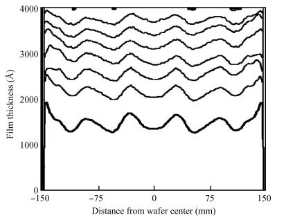
Fig. 2.  Real-time profile control.

Fig. 3.  The value of dishing and erosion.

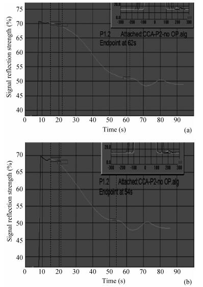
Fig. 4.  P2 endpoint of (a) slurry A and (b) slurry B.

Table 1.   Process condition of CMP.

[1]
Wang Chenwei, Liu Yuling, Tian Jianying, et al. Planarization properties of an alkaline slurry without an inhibitor on copper patterned wafer CMP. Journal of Semiconductors, 2012, 33(11):116001 doi: 10.1088/1674-4926/33/11/116001
[2]
Wang Chenwei, Liu Yuling, Niu Xinhuan, et al. An advanced alkaline slurry for barrier chemical mechanical planarization on patterned wafers. Journal of Semiconductors, 2012, 33(4):046001 doi: 10.1088/1674-4926/33/4/046001
[3]
Wang C W, Liu Y L, Tian J Y, et al. A study on the comparison of CMP performance between a novel alkaline slurry and a commercial slurry for barrier removal. Microelectron Eng, 2012, 98:29 doi: 10.1016/j.mee.2012.05.028
[4]
Wang C W, Gao J J, Tian J Y, et al. Chemical mechanical planarization of barrier layers by using a weakly alkaline slurry. Microelectron Eng, 2013, 108:71 doi: 10.1016/j.mee.2013.04.001
[5]
Cao Y, Liu Y L, Wang C W. Study on dishing control properties of an high dilution ration alkaline copper clearing slurry. International Conference on Planarization/CMP Technology, 2013:203
[6]
Nagar M, Vaes J, Ein-Eli Y. Potassium sorbate as an inhibitor in copper chemical mechanical planarization slurries. Part Ⅱ:Effects of sorbate on chemical mechanical planarization performance. Electrochimica Acta, 2010, 55:2810 doi: 10.1016/j.electacta.2009.10.086
[7]
Noh K, Saka N, Chun J H. Effect of slurry selectivity on dielectric erosion and copper dishing in copper chemical-mechanical polishing. CIRP Annals Manufacturing Technology, 2004, 53(1):463 doi: 10.1016/S0007-8506(07)60740-9
[8]
Liu X Y, Liu Y L, Liang Y, et al. Optimization of slurry components for a copper chemical mechanical polishing at low down pressure using response surface methodology. Microelectron Eng, 2011, 88:99 doi: 10.1016/j.mee.2010.09.007
[9]
Chuan L W, Liu Y L, Wang C W. Effect of back pressure on the uniformity of wafer thickness in the Cu CMP process. Micronanoelectron Technol, 2012, 49(5):340 http://en.cnki.com.cn/Article_en/CJFDTotal-BDTQ201205011.htm
[10]
Zeidler D, Plotoner M, Drescher K. Endpoint detection method for CMP of copper. Microelectron Eng, 2000, 50:411 doi: 10.1016/S0167-9317(99)00309-3
[11]
Lee H, Park B, Jeong H. Influence of slurry components on uniformity in copper chemical mechanical planarization. Microelectron Eng, 2008, 85:689 doi: 10.1016/j.mee.2007.12.044
[12]
Wang T Q, Lu X C. Numerical and experimental investigation on multi-zone chemical mechanical planarization. Microelectron Eng, 2011, 88:3327 doi: 10.1016/j.mee.2011.08.011
[13]
Nguyen V H. Daamen R, Hoofman R. Impact of different slurry and polishing pad choices on the planarization efficiency of a copper CMP process. Microelectron Eng, 2004, 76:95 doi: 10.1016/j.mee.2004.07.019
[14]
Lee H, Park B, Jeong H. Influence of slurry components on uniformity in copper chemical mechanical planarization. Microelectron Eng, 2008, 85:689 doi: 10.1016/j.mee.2007.12.044
1

Uniform, fast, and reliable CMOS compatible resistive switching memory

Yunxia Hao, Ying Zhang, Zuheng Wu, Xumeng Zhang, Tuo Shi, et al.

Journal of Semiconductors, 2022, 43(5): 054102. doi: 10.1088/1674-4926/43/5/054102

2

Effect of 1,2,4-triazole on galvanic corrosion between cobalt and copper in CMP based alkaline slurry

Lei Fu, Yuling Liu, Chenwei Wang, Linan Han

Journal of Semiconductors, 2018, 39(4): 046001. doi: 10.1088/1674-4926/39/4/046001

3

The stability of a novel weakly alkaline slurry of copper interconnection CMP for GLSI

Caihong Yao, Chenwei Wang, Xinhuan Niu, Yan Wang, Shengjun Tian, et al.

Journal of Semiconductors, 2018, 39(2): 026002. doi: 10.1088/1674-4926/39/2/026002

4

Synergic effect of chelating agent and oxidant on chemical mechanical planarization

Weijuan Liu, Yuling Liu

Journal of Semiconductors, 2015, 36(2): 026001. doi: 10.1088/1674-4926/36/2/026001

5

Influence of oxidant passivation on controlling dishing in alkaline chemical mechanical planarization

Shaohua Jia, Yuling Liu, Chenwei Wang, Chenqi Yan

Journal of Semiconductors, 2015, 36(12): 126002. doi: 10.1088/1674-4926/36/12/126002

6

Research on a processing model of CMP 6H-SiC (0001) single crystal wafer

Peng Zhang, Xianying Feng, Jingfang Yang

Journal of Semiconductors, 2014, 35(9): 096002. doi: 10.1088/1674-4926/35/9/096002

7

Surface roughness of optical quartz substrate by chemical mechanical polishing

Bo Duan, Jianwei Zhou, Yuling Liu, Mingbin Sun, Yufeng Zhang, et al.

Journal of Semiconductors, 2014, 35(11): 116001. doi: 10.1088/1674-4926/35/11/116001

8

Effect of three kinds of guanidinium salt on the properties of a novel low-abrasive alkaline slurry for barrier CMP

Guodong Chen, Yuling Liu, Xinhuan Niu

Journal of Semiconductors, 2014, 35(11): 116003. doi: 10.1088/1674-4926/35/11/116003

9

Alkaline barrier slurry applied in TSV chemical mechanical planarization

Suohui Ma, Shengli Wang, Yuling Liu, Chenwei Wang, Yan Yang, et al.

Journal of Semiconductors, 2014, 35(2): 026002. doi: 10.1088/1674-4926/35/2/026002

10

Effect of guanidine hydrochloride on removal rate selectivity and wafer topography modification in barrier CMP

Hailong Li, Jin Kang, Yuling Liu, Chenwei Wang, Hong Liu, et al.

Journal of Semiconductors, 2014, 35(3): 036002. doi: 10.1088/1674-4926/35/3/036002

11

Model analysis and experimental investigation of the friction torque during the CMP process

Guo Dongming, Xu Chi, Kang Renke, Jin Zhuji

Journal of Semiconductors, 2011, 32(3): 036002. doi: 10.1088/1674-4926/32/3/036002

12

Effects of the reciprocating parameters of the carrier on material removal rate and non-uniformity in CMP

Wang Cailing, Kang Renke, Jin Zhuji, Guo Dongming

Journal of Semiconductors, 2010, 31(12): 126001. doi: 10.1088/1674-4926/31/12/126001

13

A signal processing method for the friction-based endpoint detection system of a CMP process

Xu Chi, Guo Dongming, Jin Zhuji, Kang Renke

Journal of Semiconductors, 2010, 31(12): 126002. doi: 10.1088/1674-4926/31/12/126002

14

NiO removal of Ni/Au Ohmic contact to p-GaN after annealing

Lin Mengzhe, CaoQing, YanTingjing, ZhangShuming, ChenLianghui, et al.

Journal of Semiconductors, 2009, 30(2): 026001. doi: 10.1088/1674-4926/30/2/026001

15

Improving Carbon Nanotube Field Emission Display Luminescence Uniformity by Introducing a Reactive Current Limiting Layer

Li Xin, He Yongning, Liu Weihua, Zhu Changchun

Journal of Semiconductors, 2008, 29(3): 574-577.

16

Uniformity Investigation in 3C-SiC Epitaxial Layers Grown on Si Substrates by Horizontal Hot-Wall CVD

Li Jiaye, Zhao Yongmei, Liu Xingfang, Sun Guosheng, Luo Muchang, et al.

Chinese Journal of Semiconductors , 2007, 28(1): 1-4.

17

Control Action of Temperature on ULSI Silicon Substrate CMP Removal Rate and Kinetics Process

Liu Yuling, Niu Xinhuan, Tan Baimei, Wang Shengli

Chinese Journal of Semiconductors , 2007, 28(S1): 62-66.

18

Analysis of Factors Affecting CMP Removal Rate of Lithium Niobate

Tan Baimei, Niu Xinhuan, Han Lili, Liu Yuling, Cui Chunxiang, et al.

Chinese Journal of Semiconductors , 2007, 28(S1): 574-578.

19

CMP and Electrochemical Characterization of Ge2Sb2Te5 Filmin Polishing Slurry

Liu Qibin, Zhang Kailiang, Wang Liangyong, Song Zhitang, Feng Songlin, et al.

Chinese Journal of Semiconductors , 2006, 27(S1): 161-164.

20

CMP Slurry of Copper Interconnection for ULSI

WANG Xin, LIU Yu-ling

Chinese Journal of Semiconductors , 2002, 23(9): 1006-1008.

1. Uzhansky, M., Rakshit, A., Kalcheim, Y. et al. Coupled pyroelectric-photovoltaic effect in 2D ferroelectric α-In2Se3. npj 2D Materials and Applications, 2025, 9(1): 6. doi:10.1038/s41699-024-00523-3
2. Zhao, X., Wang, Z., Deng, X. et al. Direct Observation of Dipole Interlocking Effect Occurrence in Two-Dimensional Ferroelectricity. Nano Letters, 2025, 25(4): 1567-1574. doi:10.1021/acs.nanolett.4c05644
3. Wen, Z., Chen, J., Zhang, Q. et al. 2D Van Der Waals Ferroelectric Materials and Devices for Neuromorphic Computing. Small, 2025. doi:10.1002/smll.202412761
4. Zhao, H., Yun, J., Li, Z. et al. Two-dimensional van der Waals ferroelectrics: A pathway to next-generation devices in memory and neuromorphic computing. Materials Science and Engineering R: Reports, 2024. doi:10.1016/j.mser.2024.100873
5. Gao, L., Chen, X., Qi, J. Strain engineering of ferroelectric polarization and domain in the two-dimensional multiferroic semiconductor. Applied Physics Letters, 2024, 125(21): 212903. doi:10.1063/5.0239890
6. Chen, R.-S., Lu, Y. Negative Capacitance Field Effect Transistors based on Van der Waals 2D Materials. Small, 2024, 20(39): 2304445. doi:10.1002/smll.202304445
7. Leblanc, C., Song, S., Jariwala, D. 2D Ferroelectrics and ferroelectrics with 2D: Materials and device prospects. Current Opinion in Solid State and Materials Science, 2024. doi:10.1016/j.cossms.2024.101178
8. Bai, C., Wu, G., Yang, J. et al. 2D materials-based photodetectors combined with ferroelectrics. Nanotechnology, 2024, 35(35): 352001. doi:10.1088/1361-6528/ad4652
9. Singh, S., Kim, K.-H., Jo, K. et al. Nonvolatile Control of Valley Polarized Emission in 2D WSe2-AlScN Heterostructures. ACS Nano, 2024, 18(27): 17958-17968. doi:10.1021/acsnano.4c04684
10. Uzhansky, M., Mukherjee, S., Vijayan, G. et al. Non-Volatile Reconfigurable p–n Junction Utilizing In-Plane Ferroelectricity in 2D WSe2/α-In2Se3 Asymmetric Heterostructures. Advanced Functional Materials, 2024, 34(8): 2306682. doi:10.1002/adfm.202306682
11. Liu, Q., Cui, S., Bian, R. et al. The Integration of Two-Dimensional Materials and Ferroelectrics for Device Applications. ACS Nano, 2024, 18(3): 1778-1819. doi:10.1021/acsnano.3c05711
12. Pelella, A., Intonti, K., Viscardi, L. et al. Two-dimensional α-In2Se3 field effect transistor for wide-band photodetection and non-volatile memory. Journal of Physics and Chemistry of Solids, 2023. doi:10.1016/j.jpcs.2023.111653
13. Eom, J., Lee, I.H., Kee, J.Y. et al. Voltage control of magnetism in Fe3-xGeTe2/In2Se3 van der Waals ferromagnetic/ferroelectric heterostructures. Nature Communications, 2023, 14(1): 5605. doi:10.1038/s41467-023-41382-8
14. Lu, Y., Su, L., Fang, L. et al. Domain nucleation kinetics and polarization-texture-dependent electronic properties in two-dimensional α-In2Se3 ferroelectrics. Nanoscale, 2023, 15(45): 18306-18316. doi:10.1039/d3nr03166g
15. Pan, X., Li, Y., Cheng, B. et al. 2D materials for intelligent devices. Science China: Physics, Mechanics and Astronomy, 2023, 66(11): 117504. doi:10.1007/s11433-022-2056-1
16. Tan, C.K.Y., Fu, W., Loh, K.P. Polymorphism and Ferroelectricity in Indium(III) Selenide. Chemical Reviews, 2023, 123(13): 8701-8717. doi:10.1021/acs.chemrev.3c00129
17. Jiao, H., Wang, X., Wu, S. et al. Ferroelectric field effect transistors for electronics and optoelectronics. Applied Physics Reviews, 2023, 10(1): 011310. doi:10.1063/5.0090120
18. Chen, Z., Sun, M., Li, H. et al. Oscillatory Order-Disorder Transition during Layer-by-Layer Growth of Indium Selenide. Nano Letters, 2023, 23(3): 1077-1084. doi:10.1021/acs.nanolett.2c04785
19. Hu, C., Chen, J., Du, E. et al. Ferroelectric control of band alignments and magnetic properties in the two-dimensional multiferroic VSe2/In2Se3. Journal of Physics Condensed Matter, 2022, 34(42): 425801. doi:10.1088/1361-648X/ac8406
20. Jin, T., Mao, J., Gao, J. et al. Ferroelectrics-Integrated Two-Dimensional Devices toward Next-Generation Electronics. ACS Nano, 2022, 16(9): 13595-13611. doi:10.1021/acsnano.2c07281
21. Huang, Y.-T., Chen, N.-K., Li, Z.-Z. et al. Two-dimensional In2Se3: A rising advanced material for ferroelectric data storage. InfoMat, 2022, 4(8): e12341. doi:10.1002/inf2.12341
22. Xue, F., Ma, Y., Wang, H. et al. Two-dimensional ferroelectricity and antiferroelectricity for next-generation computing paradigms. Matter, 2022, 5(7): 1999-2014. doi:10.1016/j.matt.2022.05.021
23. Wei, X.-K., Domingo, N., Sun, Y. et al. Progress on Emerging Ferroelectric Materials for Energy Harvesting, Storage and Conversion. Advanced Energy Materials, 2022, 12(24): 2201199. doi:10.1002/aenm.202201199
24. Huang, W., Song, M., Zhang, Y. et al. Chemical vapor deposition growth of nonlayered γ-In2Se3 nanosheets on SiO2/Si substrates and its photodetector application. Journal of Alloys and Compounds, 2022. doi:10.1016/j.jallcom.2022.164010
25. Weston, A., Castanon, E.G., Enaldiev, V. et al. Interfacial ferroelectricity in marginally twisted 2D semiconductors. Nature Nanotechnology, 2022, 17(4): 390-395. doi:10.1038/s41565-022-01072-w
26. Mukherjee, S., Koren, E. Indium Selenide (In2Se3) – An Emerging Van-der-Waals Material for Photodetection and Non-Volatile Memory Applications. Israel Journal of Chemistry, 2022, 62(3-4): e202100112. doi:10.1002/ijch.202100112
27. Zhang, Z., Nie, J., Zhang, Z. et al. Atomic Visualization and Switching of Ferroelectric Order in β-In2Se3 Films at the Single Layer Limit. Advanced Materials, 2022, 34(3): 2106951. doi:10.1002/adma.202106951
28. Zhang, Y., Wang, L., Chen, H. et al. Analog and Digital Mode α-In2Se3 Memristive Devices for Neuromorphic and Memory Applications. Advanced Electronic Materials, 2021, 7(12): 2100609. doi:10.1002/aelm.202100609
29. Chen, Z., Fu, W., Wang, L. et al. Atomic Imaging of Electrically Switchable Striped Domains in β′-In2Se3. Advanced Science, 2021, 8(17): 2100713. doi:10.1002/advs.202100713
30. Liang, Y., Shen, S., Huang, B. et al. Intercorrelated ferroelectrics in 2D van der Waals materials. Materials Horizons, 2021, 8(6): 1683-1689. doi:10.1039/d1mh00446h
31. Xue, F., He, J.-H., Zhang, X. Emerging van der Waals ferroelectrics: Unique properties and novel devices. Applied Physics Reviews, 2021, 8(2): 021316. doi:10.1063/5.0028079
32. Kim, J.Y., Choi, M.-J., Jang, H.W. Ferroelectric field effect transistors: Progress and perspective. APL Materials, 2021, 9(2): 0035515. doi:10.1063/5.0035515
33. Zhang, J., Xue, W., Chen, X.-Y. et al. Sm doped BiFeO3 nanofibers for improved photovoltaic devices. Chinese Journal of Physics, 2020. doi:10.1016/j.cjph.2020.03.021
34. Chen, J.-D., Han, W.-H., Yang, C. et al. Recent research progress of ferroelectric negative capacitance field effect transistors | [铁电负电容场效应晶体管研究进展]. Wuli Xuebao/Acta Physica Sinica, 2020, 69(13): 137701. doi:10.7498/aps.69.20200354
35. Zhang, J., Ma, P., Shi, T. et al. Nd-Cr co-doped BiFeO3 thin films for photovoltaic devices with enhanced photovoltaic performance. Thin Solid Films, 2020. doi:10.1016/j.tsf.2020.137852
  • Search

    Advanced Search >>

    GET CITATION

    Yue Li, Ming Gong, Hualing Zeng. Atomically thin α-In2Se3: an emergent two-dimensional room temperature ferroelectric semiconductor[J]. Journal of Semiconductors, 2019, 40(6): 061002. doi: 10.1088/1674-4926/40/6/061002
    Y Li, M Gong, H L Zeng, Atomically thin α-In2Se3: an emergent two-dimensional room temperature ferroelectric semiconductor[J]. J. Semicond., 2019, 40(6): 061002. doi: 10.1088/1674-4926/40/6/061002.
    shu

    Export: BibTex EndNote

    Article Metrics

    Article views: 2683 Times PDF downloads: 19 Times Cited by: 35 Times

    History

    Received: 14 February 2014 Revised: 12 March 2014 Online: Published: 01 September 2014

    Catalog

      Email This Article

      User name:
      Email:*请输入正确邮箱
      Code:*验证码错误
      Yue Li, Ming Gong, Hualing Zeng. Atomically thin α-In2Se3: an emergent two-dimensional room temperature ferroelectric semiconductor[J]. Journal of Semiconductors, 2019, 40(6): 061002. doi: 10.1088/1674-4926/40/6/061002 ****Y Li, M Gong, H L Zeng, Atomically thin α-In2Se3: an emergent two-dimensional room temperature ferroelectric semiconductor[J]. J. Semicond., 2019, 40(6): 061002. doi: 10.1088/1674-4926/40/6/061002.
      Citation:
      Weijuan Liu, Yuling Liu, Chenwei Wang, Guodong Chen, Mengting Jiang, Haobo Yuan, Pengfei Cheng. Effect of novel alkaline copper slurry on 300 mm copper global planarization[J]. Journal of Semiconductors, 2014, 35(9): 096003. doi: 10.1088/1674-4926/35/9/096003 ****
      W J Liu, Y L Liu, C W Wang, G D Chen, M T Jiang, H B Yuan, P F Cheng. Effect of novel alkaline copper slurry on 300 mm copper global planarization[J]. J. Semicond., 2014, 35(9): 096003. doi: 10.1088/1674-4926/35/9/096003.

      Effect of novel alkaline copper slurry on 300 mm copper global planarization

      DOI: 10.1088/1674-4926/35/9/096003
      Funds:

      the Major National Science and Technology Special Projects 2009ZX02308

      Project supported by the Major National Science and Technology Special Projects (No. 2009ZX02308)

      More Information
      • Corresponding author: Liu Weijuan, Email:269227849@qq.com
      • Received Date: 2014-02-14
      • Revised Date: 2014-03-12
      • Published Date: 2014-09-01

      Catalog

        /

        DownLoad:  Full-Size Img  PowerPoint
        Return
        Return