Processing math: 100%
J. Semicond. > 2015, Volume 36 > Issue 1 > 016002

SEMICONDUCTOR TECHNOLOGY

Next generation barrier CMP slurry with novel weakly alkaline chelating agent

Shiyan Fan1, 2, , Yuling Liu1, Ming Sun1, Jiying Tang1, Chenqi Yan1, Hailong Li1 and Shengli Wang1

+ Author Affiliations

 Corresponding author: Shiyan Fan, E-mail: 494866895@qq.com

DOI: 10.1088/1674-4926/36/1/016002

PDF

Abstract: To strengthen the device performance with the pattern wafer by enhancing the Cu polishing rate and improve the surface roughness with the Cu lines, a new weakly alkaline chelating agent with a barrier slurry is developed to meet the process demand of the advanced barrier chemical mechanical planarization (CMP). This new chelating agent has a stronger chelating ability and a lower pH value than the previous generation-FA/O I chelating agent researched before. Without an unstable oxidant agent added in the polishing slurry, it is difficult to enhance the copper polishing rate during the barrier CMP. The stronger chelating ability of the new chelating agent could increase the copper polishing rate along with controlling the Cu/Ta/TEOS removal rate selectivity to meet the requirements of the IC fabrication process. Thus it has solved the problem of excessive roughness due to the lower polishing rate, avoiding reducing the device performance with the pattern wafer. The new chelating agent with its lower pH value could make it possible to protect the low-k dielectric under the barrier layer from structurally breaking. The CMP experiment was performed on the 12 inch MIT 854 pattern wafers with the barrier slurry containing the new weakly alkaline chelating agent. By the DOE optimization, the results indicate that as the new chelating agent concentration in the slurry was up to 2.5 mL/L, the copper polishing rate is about 31.082 nm/min. Meanwhile, the wafer surface has a rather low roughness value of 0.693 nm (10 × 10 μm), the correction ability with the above slurry is adapted to the next generation barrier CMP and the k value of the low-k dielectric seems to have no k-shift. All the results presented show that the new weakly alkaline chelating agent with its superior performance can be used for the advanced barrier CMP.

Key words: barrier CMPchelating agentpolishing ratesurface roughness

In the process of mining, industrial production and transportation, toxic, explosive and corrosive gases are often produced[1]. To ensure the quality of products and safety in the production process, real-time monitoring of gas components, concentrations, and other parameters plays an important role[2, 3]. It is worth mentioning that semiconductor lasers emitting at 1.6–1.9 μm with the strong absorption lines of various gases, such as ethylene, methane, hydrogen chloride, and nitric oxide, have gained a lot of interest for working as the light source on gas sensing[4-6]. Combined with the requirements of gas sensing, several wavelength tunable semiconductor lasers are proposed and fabricated, like distributed feedback (DFB) lasers[4, 7, 8], distributed Bragg reflector (DBR) lasers[9-13], and vertical cavity surface emitting lasers (VCSELs)[14-16]. The mode selection of DFB and DBR lasers is based on Bragg grating, which requires fine etching and regrowth process. The VCSELs are based on the DBR structure composed of multilayer materials. Therefore, these lasers always require either fine fabrication technology or complex epitaxial structure, which caused high fabrication costs. Hybrid cavity lasers[17-20] can realize wavelength tuning without etching grating, which have attracted people's attention. We noticed that a kind of hybrid cavity semiconductor laser based on a Whispering-Gallery (WG) microcavity and a Fabry–Pérot (FP) cavity, was able to realize a larger wavelength tunable range while with lower cost[21-23]. Due to short cavity length, it is easy to realize single longitudinal mode operation for microcavity lasers. However, a conventional FP cavity laser is usually multiple longitudinal lasing. The hybrid cavity composed of an FP cavity and a square microcavity has been demonstrated for mode selection by enhancing the mode Q factor for hybrid mode between the WG and FP mode. Stable single-mode operation is realized by injecting currents to the square microcavity and the FP cavity sections at the same time[24]. However, the existing WG-FP hybrid cavity lasers are basically emitting at the C band, which are used in optical communication but are barely used in gas sensing.

Therefore, in this paper, we report a single-mode WG-FP hybrid cavity laser with a wide wavelength tuning range from 1760.87 to 1773.39 nm. The side-mode suppression ratio (SMSR) for the whole tuning range is over 30 dB. And the lasing output power was over 3.5 mW at 20 °C. Compared with the DFB lasers, DBR lasers, and VCSELs, the hybrid cavity laser does not introduce the grating etching process and complex epitaxial structure, which can reduce the fabrication difficulty and cost. And the over –12.5 nm tuning range incorporates absorption lines of methane and hydrogen chloride[25], showing a practical perspective for gas sensing with this hybrid-cavity laser.

Aiming to study the mode characteristics of the WG-FP hybrid cavity laser, a systematic numerical simulation based on the two-dimensional (2D) finite element method (FEM) was adopted[26]. The setting of simulation parameters is shown in Fig. 1. The refractive indices of the hybrid cavity, the bisbenzocyclobutene (BCB) which surrounds the cavities are 3.2 and 1.54, respectively. In practice, the light emits directly into the air from the end of the FP cavity, therefore, an air layer is added with a refractive index of 1. The WG-FP hybrid cavity laser consists of a square microcavity with the side length a = 20 μm, and an FP cavity with the length L = 360 μm, the width w = 3 μm. The perfectly matched layer (PML) is set as the boundary condition because it can absorb all the scattered light to simulate an infinite space, which is consistent with reality. After building the simulation model, we simulated the mode Q factors, field distributions, and far-field behaviors under different eigenfrequency by calculating the characteristic solution f of Maxwell's characteristic equation.

Figure  1.  (Color online) The simulation parameters of the WG-FP hybrid cavity laser.

To explore the influence of square microcavity on lasing mode selection, mode Q factor that varied with different mode wavelengths was simulated, as shown in Fig. 2, where the Q factor can be defined as [27]:

Figure  2.  (Color online) The mode Q factor variation with different mode wavelength when (a) Im(nWG) = Im(nFP) = 0. (b) Im(nWG) decreases from 0.00003 to –0.00003 while Im(nFP) = 0.
Q=Re(f)2|Im(f)|. (1)

Referring to Fig. 2(a),the mode Q factor in the WG-FP hybrid cavity fluctuated periodically, and the Q factors were significant at the mode wavelengths of 1747.8, 1764.8, and 1782.2 nm. Based on the relationship between the gain coefficient g and the imaginary part of the refractive index Im(n) [28]:

g=2ωIm(n)c=4πIm(n)λ, (2)

where ω is the angular frequency of light waves, c is the speed of light, and λ is the wavelength of light waves.

The relationship between Q factor and gain of the mode wavelength at 1764.8 nm was explored. By changing the imaginary part of the refractive index of the square microcavity Im(nWG), while keeping the imaginary part of the refractive index of the FP cavity Im(nFP) = 0, the change of the mode Q factor was studied with the imaginary part of the refractive index of the square microcavity changed. As shown in Fig. 2(b), as Im(nWG) decreased from 3 × 10⁻⁵ to –3 × 10⁻⁵, which means the gain coefficient increased from –2.1 to 2.1 cm–1, the mode Q factor near the mode wavelength of 1764.8 nm increased with the improvement of the gain coefficient, which showed low sensitivity to the variation of Im(nWG) at other mode wavelengths. We infer that the mode at 1764.8 nm is the coupling mode of the square microcavity and the FP cavity.

To study the center wavelength tuning ability of the laser, we changed the real part of the refractive index of the square cavity Re(nWG) to characterize the change of the laser when the working current is applied. As shown in Fig. 3, the mode center wavelengths with the change of the index ΔnWG were simulated. It can be found that as the refractive index increased, the mode center wavelength of the laser gradually redshifted.

Figure  3.  The mode center wavelengths variation with the change of the real part of the square microcavity refractive index ΔnWG.

In this paper, the materials of the devices were grown by metal organic chemical vapor deposition (MOCVD) equipment. Combined with the experiences of material epitaxy in our group[5, 7, 10], we chose InGaAs/InGaAsP multi-quantum wells (MQWs) as the active region and the whole material structure was epitaxially grown on an n-type InP substrate. The strained MQW consisted of four pairs of 9.5 nm compressively strained InGaAs wells and 12 nm five tensile strained InGaAsP barriers embedded in two undoped InGaAsP (λPL = 1.3 μm, where PL stands for photoluminescence) separate confinement layers (SCH). A 1700 nm InP layer with a lower refractive index used for limiting the light field, formed the upper cladding layer. A 200 nm InGaAs was deposited on the top of the whole structure as a contact layer.

Compared with DFB and DBR lasers, the WG-FP hybrid cavity laser does not need to etch grating, which reduces regrowth processes, simplifies the fabrication process, and reduces the cost. The fabrication process of the WG-FP hybrid cavity laser is shown in Fig. 4. Standard contacting photolithography and the inductively coupled plasma (ICP) etching method were adopted to ensure the quality of the cavity. As shown in Fig. 5(a), the sidewall was supposed to be vertical and smooth. To reduce the light leakage to the substrate, the etching depth was greater than 4.5 μm, which meant the quantum well region was exposed. SiO2 and BCB layers were deposited and coated to protect the active region from oxidation and electric leakage, and a large area of reactive ion etching (RIE) was performed then to expose the top of the contact layer for depositing the electrode metal. To guarantee the two cavities will be electrically isolated from each other, the p-InGaAs contact layer should be removed. Therefore, a shallow isolation trench of about 300 nm in depth and 5 μm in width was formed by wet etching. This depth is far from the active region and the waveguide layer, which will not affect the mode characteristics of the device. At last, Ti/Au and AuGeNi/Au were deposited to form p and n type electrodes respectively. The microscope image of the fabricated WG-FP hybrid cavity laser was shown in Fig. 5(b), two rectangular p-type electrodes are used for current injection into the two cavities separately.

Figure  4.  (Color online) Fabrication process of the WG-FP hybrid cavity laser.
Figure  5.  (Color online) (a) Cross-sectional view SEM image after ICP etching. (b) The microscope image of the fabricated WG-FP hybrid cavity laser.

The hybrid-cavity was mounted on a Cu submount with the p-side upward and was tested under continuous-wave (CW) at 20 °C. To ensure that the two cavities were electrically isolated from each other, we tested the I–V curve. The isolation resistance is about 25 kΩ as calculated, which was enough to achieve the electrical isolation[21]. For a WG-FP hybrid cavity laser with dimensions of a = 20 μm, L = 360 μm, w = 3 μm, the output power was collected by an integrating sphere. Light power varied with the injection currents of the FP cavity (IFP) curves were plotted in Fig. 6 (a) under the injection currents of the WG cavity (IWG) at 0, 2, 5, and 10 mA. Owing to the WG cavity did not work when IWG = 0 mA, the laser did not emit. The threshold current Ith reduced from 42 to 30 mA and the output power increased from 2.1 to 3.6 mW, as shown in Fig. 6(a), when IFP increased to 60 mA and IWG increased from 2 to 10 mA, which showed the positive feedback effect from the square microcavity. This was due to the improvement of the mode Q factor for the hybrid mode, which was in accord with the trend of simulation in Fig. 2. The slope efficiencies were estimated to be about 0.116 W/A when IWG = 10 mA, IFP = 60 mA, respectively. The dependence of threshold current on temperature was shown in the inset of Fig. 6(b). Basing on the empirical relation, Ith = I0exp(T/T0), a characteristic temperature (T0) was calculated as 44.3 K at 20 °C after fitting.

Figure  6.  (Color online) (a) Curves of light power variation with IFP at the IWG are 0, 2, 5, and 10 mA. (b) Lasing spectrum measured for the laser under IFP = 80 mA, IWG = 70 mA.

The emitting light was partially collected by a tapered fiber and transmitted to an optical spectrum analyzer with a resolution of 0.05 nm through a single-mode fiber. Lasing spectrum measured for the laser under IFP = 80 mA, IWG = 70 mA was shown in Fig. 6(b). The laser emitted as a single mode with the side-mode suppression ratio (SMSR) of 33.79 dB. As shown in Figs. 7(a) and 7(c), when IFP = 80 mA, the center wavelength redshifted from 1761.52 to 1771.63 nm (10.11 nm) with the SMSRs over 28 dB, as the IWG continuously increased from 5 to 88 mA. As shown in Figs. 7(b) and 7(d), when IWG = 35 mA, the center wavelength redshifted from 1762.32 to 1763.05 nm (0.73 nm) with SMSRs over 32 dB, as the IFP continuously increased from 40 to 80 mA. Owing to the small size of the square microcavity, it is more sensitive to the changes of temperature and refractive index. Therefore, the square cavity has a greater influence on the wavelength change which can be used for coarse tuning, while the FP cavity can be used for fine-tuning.

Figure  7.  (Color online) Lasing characteristics with the variations of IFP and IWG for the laser. Lasing spectra (a) variation with IWG at IFP = 80 mA, (b) variation with IFP at IWG = 35 mA. Dominant lasing mode wavelengths and corresponding SMSRs (c) variation with IWG at IFP = 80 mA, (d) variation with IFP at IWG = 35 mA, respectively.

By varying the injected current of the square cavity and FP cavity simultaneously, the wavelength tuning range of 12.52 nm from 1760.87 to 1773.39 nm was realized, and the SMSRs were above 30 dB for the whole course. The superimposed lasing spectrum is shown in Fig. 8. Compared with the previous works[5, 10, 25, 27], the wavelength tuning range has been improved.

Figure  8.  (Color online) Superimposed lasing spectra with a wavelength continuous tuning range of 12.52 nm by varying IFP and IWG simultaneously.

In conclusion, a hybrid-cavity laser consisting of a square Whispering-Gallery microcavity and a Fabry–Pérot was demonstrated. The output power was over 3.5 mW and a wavelength tuning range over 12.5 nm were obtained. Besides, the laser performed single-mode emitting with the side-mode suppression ratio over 30 dB. Light-emitting range from 1760.87 to 1773.39 nm corresponds to the absorption lines of methane and hydrogen chloride. Moreover, grating etching process and complex epitaxial structure were not introduced into the fabrication process, which reduced the manufacturing difficulty and cost while achieving a wide wavelength tuning range as well. Thus, the device yield will be improved, and it is more conducive to production. Therefore, the WG-FP hybrid cavity laser illustrated a practical perspective for certain purposes of gas sensing.

This work was supported by the National Key Research and Development Program of China (Grant No. 2018YFA0209001), the Key Project of Frontier Science Research Project of CAS (Grant No. QYZDY-SSW-JSC021), and the Strategic Priority Research Program of CAS (Grant No. XDB43020202).


[1]
[2]
[3]
[4]
[5]
[6]
[7]
[8]
[9]
[10]
[11]
[12]
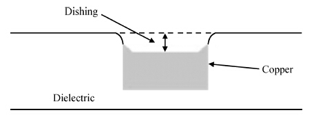
Fig. 1.  Schematic~diagram of dishing.

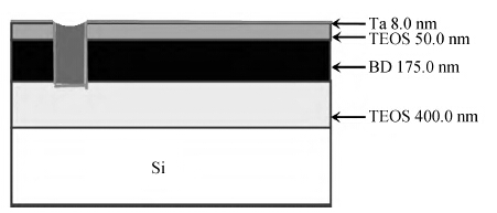
Fig. 2.  Cross-section view of a 12 inch pattern wafer.

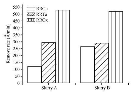
Fig. 3.  Cu/Ta/TEOS(Ox) polishing rate using slurries containing two kinds of chelating agent.

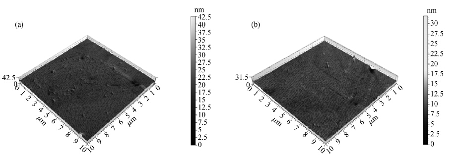
Fig. 4.  The surface roughness of copper wafer with the two slurries.

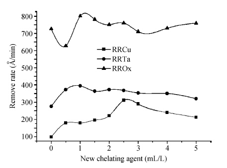
Fig. 5.  Cu/Ta/TEOS polishing speed as the concentration of the new weakly chelating agent changed.

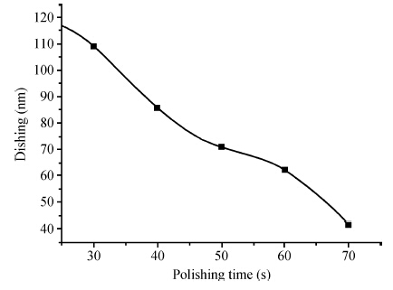
Fig. 6.  The dishing data post barrier polishing with the new weakly alkaline chelating agent.

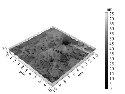
Fig. 7.  The surface roughness of the pattern wafer before barrier CMP.

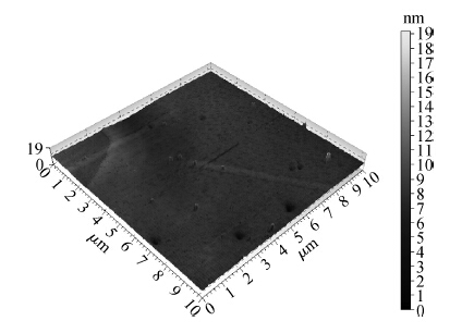
Fig. 8.  The surface roughness of the pattern wafer post barrier CMP using the new chelating agent.

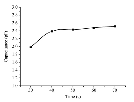
Fig. 9.  The capacitance of the interconnect wiring as a function of polishing time.

Table 1.   3-inch blanket wafer polishing process.

DownLoad: CSV

Table 2.   12-inch pattern wafer polishing process.

DownLoad: CSV
[1]
[2]
[3]
[4]
[5]
[6]
[7]
[8]
[9]
[10]
[11]
[12]
1

Influence of precursor solution concentration on the structural, optical and humidity sensing properties of spray-deposited TiO2 thin films

Dipak L Gapale, Sandeep A Arote, Balasaheb M Palve, Ratan Y Borse

Journal of Semiconductors, 2018, 39(12): 122003. doi: 10.1088/1674-4926/39/12/122003

2

A simple chemical route to synthesize the umangite phase of copper selenide (Cu3Se2) thin film at room temperature

Balasaheb M. Palve, Sandesh R. Jadkar, Habib M. Pathan

Journal of Semiconductors, 2017, 38(6): 063003. doi: 10.1088/1674-4926/38/6/063003

3

Energy-efficient digital and wireless IC design for wireless smart sensing

Jun Zhou, Xiongchuan Huang, Chao Wang, Tony Tae-Hyoung Kim, Yong Lian, et al.

Journal of Semiconductors, 2017, 38(10): 105005. doi: 10.1088/1674-4926/38/10/105005

4

Synthesis of metal oxide composite nanosheets and their pressure sensing properties

Muhammad Tariq Saeed Chani, Sher Bahadar Khan, Kh. S. Karimov, M. Abid, Abdullah M. Asiri, et al.

Journal of Semiconductors, 2015, 36(2): 023002. doi: 10.1088/1674-4926/36/2/023002

5

Analytical modeling and simulation of germanium single gate silicon on insulator TFET

T. S. Arun Samuel, N. B. Balamurugan

Journal of Semiconductors, 2014, 35(3): 034002. doi: 10.1088/1674-4926/35/3/034002

6

Giant magnetoresistance in a two-dimensional electron gas modulated by ferromagnetic and Schottky metal stripes

Lu Jianduo, Xu Bin

Journal of Semiconductors, 2012, 33(7): 074007. doi: 10.1088/1674-4926/33/7/074007

7

Optical and electrical properties of electrochemically deposited polyaniline-CeO2 hybrid nanocomposite film

Anees A. Ansari, M. A. M. Khan, M. Naziruddin Khan, Salman A. Alrokayan, M. Alhoshan, et al.

Journal of Semiconductors, 2011, 32(4): 043001. doi: 10.1088/1674-4926/32/4/043001

8

Thermal analysis and test for single concentrator solar cells

Cui Min, Chen Nuofu, Yang Xiaoli, Wang Yu, Bai Yiming, et al.

Journal of Semiconductors, 2009, 30(4): 044011. doi: 10.1088/1674-4926/30/4/044011

9

Numerical analysis of four-wave-mixing based multichannel wavelength conversion techniques in fibers

Jia Liang, Zhang Fan, Li Ming, Liu Yuliang, Chen Zhangyuan, et al.

Journal of Semiconductors, 2009, 30(5): 054007. doi: 10.1088/1674-4926/30/5/054007

10

A widely tunable continuous-time LPF for a direct conversion DBS tuner

Chen Bei, Chen Fangxiong, Ma Heping, Shi Yin, Dai F F, et al.

Journal of Semiconductors, 2009, 30(2): 025009. doi: 10.1088/1674-4926/30/2/025009

11

Quantum and Transport Mobilities of a Two-Dimensional Electron Gas in the Presence of the Rashba Spin-Orbit Interaction

Xu Wen

Chinese Journal of Semiconductors , 2006, 27(2): 204-217.

12

Analysis of PTCDA/ITO Surface and Interface Using X-ray Photoelectron Spectroscopy and Atomic Force Microscopy

Tang Ning, Shen Bo, Wang Maojun, Yang Zhijian, Xu Ke, et al.

Chinese Journal of Semiconductors , 2006, 27(2): 235-238.

13

Analysis of PTCDA/ITO Surface and Interface Using X-ray Photoelectron Spectroscopy and Atomic Force Microscopy

Ou Guping, Song Zhen, Gui Wenming, Zhang Fujia

Chinese Journal of Semiconductors , 2006, 27(2): 229-234.

14

Temperature Dependence of Vacuum Rabi Splitting in a Single Quantum Dot-Semiconductor Microcavity

Zhu Kadi, Li Waisang

Chinese Journal of Semiconductors , 2006, 27(3): 489-493.

15

Single Mode Operation of Short-Cavity Quantum Cascade Lasers

Liu Fengqi, Guo Yu, Li Lu, Shao Ye, Liu Junqi, et al.

Chinese Journal of Semiconductors , 2006, 27(4): 679-682.

16

Passively Mode Locked Diode-End-Pumped Yb∶YAB Laser with High Reflectivity Type Semiconductor Saturable Absorption Mirror

Wang Yonggang, Ma Xiaoyu, Xue Yinghong, Sun Hong,Zhang Zhigang,and Wang Qingyue

Chinese Journal of Semiconductors , 2005, 26(2): 250-253.

17

A Broadband Long-Wavelength Superluminescent Diode Based on Graded Composition Bulk InGaAs

Ding Ying, Wang Wei, Kan Qiang, Wang Baojun, Zhou Fan, et al.

Chinese Journal of Semiconductors , 2005, 26(12): 2309-2314.

18

AIN Monolithic Microchannel Cooled Heatsink for High Power Laser Diode Array

Ma Jiehui, Fang Gaozhan, Lan Yongsheng and, Ma Xiaoyu

Chinese Journal of Semiconductors , 2005, 26(3): 476-479.

19

A Wavelength Tunable DBR Laser Integrated with an Electro-Absorption Modulator by a Combined Method of SAG and QWI

Zhang Jing, Li Baoxia, Zhao Lingjuan, Wang Baojun, Zhou Fan, et al.

Chinese Journal of Semiconductors , 2005, 26(11): 2053-2057.

20

A Novel Two-Section Co-Cavity Wavelength Tunable Sem iconductor Laser

Chinese Journal of Semiconductors , 1999, 20(9): 816-822.

  • Search

    Advanced Search >>

    GET CITATION

    Fangyuan Meng, Hongyan Yu, Xuliang Zhou, Mengqi Wang, Yejin Zhang, Wenyu Yang, Jiaoqing Pan. Low fabrication cost wavelength tunable WG-FP hybrid-cavity laser working over 1.7 μm[J]. Journal of Semiconductors, 2022, 43(6): 062302. doi: 10.1088/1674-4926/43/6/062302
    F Y Meng, H Y Yu, X L Zhou, M Q Wang, Y J Zhang, W Y Yang, J Q Pan. Low fabrication cost wavelength tunable WG-FP hybrid-cavity laser working over 1.7 μm[J]. J. Semicond, 2022, 43(6): 062302. doi: 10.1088/1674-4926/43/6/062302
    shu

    Export: BibTex EndNote

    Article Metrics

    Article views: 2424 Times PDF downloads: 26 Times Cited by: 0 Times

    History

    Received: 08 June 2014 Revised: Online: Published: 01 January 2015

    Catalog

      Email This Article

      User name:
      Email:*请输入正确邮箱
      Code:*验证码错误
      Fangyuan Meng, Hongyan Yu, Xuliang Zhou, Mengqi Wang, Yejin Zhang, Wenyu Yang, Jiaoqing Pan. Low fabrication cost wavelength tunable WG-FP hybrid-cavity laser working over 1.7 μm[J]. Journal of Semiconductors, 2022, 43(6): 062302. doi: 10.1088/1674-4926/43/6/062302 ****F Y Meng, H Y Yu, X L Zhou, M Q Wang, Y J Zhang, W Y Yang, J Q Pan. Low fabrication cost wavelength tunable WG-FP hybrid-cavity laser working over 1.7 μm[J]. J. Semicond, 2022, 43(6): 062302. doi: 10.1088/1674-4926/43/6/062302
      Citation:
      Shiyan Fan, Yuling Liu, Ming Sun, Jiying Tang, Chenqi Yan, Hailong Li, Shengli Wang. Next generation barrier CMP slurry with novel weakly alkaline chelating agent[J]. Journal of Semiconductors, 2015, 36(1): 016002. doi: 10.1088/1674-4926/36/1/016002 ****
      S Y Fan, Y L Liu, M Sun, J Y Tang, C Q Yan, H L Li, S L Wang. Next generation barrier CMP slurry with novel weakly alkaline chelating agent[J]. J. Semicond., 2015, 36(1): 016002. doi: 10.1088/1674-4926/36/1/016002.

      Next generation barrier CMP slurry with novel weakly alkaline chelating agent

      DOI: 10.1088/1674-4926/36/1/016002
      Funds:

      Project supported by the Special Project Items No. 2 in National Long-Term Technology Development Plan, China (No. 2009ZX02308) and the Natural Science Foundation of Hebei Province, China (No. E2014202147).

      More Information
      • Corresponding author: E-mail: 494866895@qq.com
      • Received Date: 2014-06-08
      • Accepted Date: 2014-06-26
      • Published Date: 2015-01-25

      Catalog

        /

        DownLoad:  Full-Size Img  PowerPoint
        Return
        Return