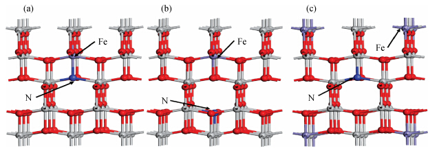
J. Semicond. > 2015, Volume 36 > Issue 10 > 102003

SEMICONDUCTOR PHYSICS

Effect of N and Fe codoping on the electronic structure and optical properties of TiO2 from first-principles study

Zhuomao Zhu1, Baoan Bian1 and Haifeng Shi1, 2

+ Author Affiliations
DOI: 10.1088/1674-4926/36/10/102003

PDF

Abstract: The electronic structure and optical properties of N and Fe codoping TiO2 have been investigated by first-principles calculations based on density functional theory.The calculated results indicate that the stability of N and Fe codoping TiO2 will change at different substitutional sites of N and Fe.The mechanism of band gap narrowing of doping TiO2 is discussed by investigating the density of state.The different substitutional site of N and Fe in codoping TiO2 influences the visible-light absorption.An increased visible-light absorption for doping TiO2 results from the synergistic effect of N and Fe codoping.Therefore, N and Fe codoping may enhance the visible-light photocatalytic activity of TiO2.

Key words: codopingfirst-principleelectronic structureoptical properties

Post-transition-metal oxides, such as In2O3 and SnO2, have been extensively used as transparent conducting oxides (TCOs), a unique class of materials that combine the high electrical conductivity and optical transmission in the visible or near-infrared spectral range, which are needed in various optoelectronic devices, such as solar cells, flat-panel displays, light emitting diodes (LEDs) and transparent transistors[1-7]. Obviously, one of the most critical properties of these materials is related to their band gaps that essentially determine their transparency. However, the determination of band gaps of these TCOs has not been a trivial work. For instance, early experimental measurements on In2O3 revealed a strong optical absorption at 3.75 eV and a much weaker absorption at 2.62 eV[8]. Initially, the former absorption was attributed as the direct band gap of In2O3, while the latter was attributed to the indirect transitions. Although this interpretation seems able to explain some of the experiments, the indirect transitions in In2O3 has never been confirmed by first-principles calculations[9, 10], hindering further understanding of the band structure and optical properties of this material. More recently, by combining the experimental measurements and theoretical calculations, Walsh et al.[11] identified that In2O3 actually possesses a direct fundamental gap of 2.9 eV and a much larger optical gap of 3.7 eV. The large discrepancy between the fundamental and optical gaps was attributed to the inversion symmetry of its bixbyite structure and the resultant dipole-forbidden transitions between the valence band maximum (VBM) and conduction band minimum (CBM) states. This argument, capable of explaining various theoretical and experimental results, has now been commonly accepted.

In contrast to the case of In2O3, the band gap problem of SnO2 is still not fully understood, largely because of the lack of detailed experimental measurements. Analogous to bixbyite In2O3, rutile SnO2 also has the inversion symmetry and the dipole-forbidden transitions between the band edge states. As a result, one may expect different fundamental and optical gaps of SnO2 as well, which, however, has never been reported in experiments. The single-photon and two-photon absorption experiments showed an optical gap of SnO2 at ~3.60 eV, which has been widely taken as its “band gap”[12-14]. Moreover, the recent theoretical calculations, based on the density functional theory (DFT) and GW approximation, identified a fundamental gap of 3.65 eV for SnO2[15, 16], which is nearly equal to its optical gap. Sabino et al.[17] attributed the coincidence between the measured fundamental and optical gaps to the intense illumination used in experiments, so that the very weak absorption in the vicinity of Γ point at the band edges was detected. Based on this argument, they also predicted that a much larger optical band gap of 4.34 eV should be detected, if the low illumination condition is satisfied. However, up to now, no experimental demonstration of this difference between fundamental and optical gaps has been reported.

Despite the absence of direct measurements on its fundamental gap, more insight can be obtained from the recent experiments where SnO2 was employed as the electron transport layer (ETL) in both dye-sensitized and perovskite solar cells to replace the commonly used TiO2[18, 19]. The band alignment measurements[19] showed that the CBM of SnO2 is about 0.4 eV lower than that of TiO2, which facilitates the electron transport. Assuming the fundamental gaps of SnO2 and TiO2 as 3.65 and 3.03 eV[20], respectively, we can easily deduce that the VBM of SnO2 is ~1.02 eV lower than that of TiO2, as illustrated in Fig. 1(a). This result, however, is quite puzzling and contradicts the small VBM offset one would expect in this system[21-23], because the two compounds are isovalent semiconductors with the same rutile structure and similar lattice constants, and moreover, the Γ3+ VBM state is almost a pure oxygen p state, which only couples weakly with the cation d state but does not couple to the cation p state. Therefore, this VB offset anomaly is difficult to understand if the fundamental gap of SnO2 is taken as ~3.65 eV, as previously reported.

Figure  1.  (Color online) Band gaps and band alignments between rutile SnO2 and TiO2. In (a) the band gaps of SnO2 is taken from Ref. [15] and the CB band alignment is taken from Ref. [19], while in (b) both of them are calculated in this work. The band gap of TiO2 is always set to its experimental value (taken from Ref. [20]).

To address this issue, in this work, we revisit the band gap problem for the rutile SnO2 by using first-principles calculations. Different-level computational methods and functionals, such as PBE, PBE + G0W0, HSE06 and HSE06 + G0W0 are employed and the results are carefully compared. We find that the HSE06 calculations yield a VB offset of 0.38 eV between SnO2 and TiO2, generally obeying the common-anion rule. The fundamental gap is calculated to be 2.96 eV, which is much smaller than the previously reported value. The conduction band (CB) offset is then found to be 0.45 eV, in good agreement with experiments[18, 19]. Moreover, similar to In2O3, our calculations reveal that the direct optical transition between the band edges of SnO2 is parity forbidden and the optical gap between the lower-lying VB states and CBM is 3.69 eV, which can well explain its optical absorptions[12-14]. On the other hand, by employing the HSE06 + G0W0 method, the fundamental gap of SnO2 is found to be 3.76 eV that is close to the value reported previously[16, 17, 24]. However, with the same method, the fundamental gap of TiO2 is calculated to be 3.68 eV, significantly larger than the experimental result of 3.03 eV[20]. In fact, we find that the fundamental gap of SnO2 is always similar to that of TiO2, independent of the computational methods and functionals employed, which implies that the HSE06 + G0W0 calculations may overestimate the fundamental gap of SnO2, which has been the case also found in other sp semiconductors[25]. The estimated error of HSE06 + G0W0 calculation is about 0.8 eV, which in turn results in a fundamental gap of SnO2 as ~3.0 eV, in good agreement with the HSE06 calculations.

Our calculations are carried out using the projector augmented wave (PAW) method[26] and the Heyd–Scuseria–Ernzerhof (HSE06) hybrid functional[27] within the density functional theory (DFT) as implemented in VASP[28]. For both SnO2 and TiO2, a 520 eV cutoff energy is used for the plane wave basis set and a Γ-centered 4 × 4 × 6 k-point sampling of the Brillouin zone is employed. Since the band gaps of these compounds are sensitive to their lattice constants, experimental lattice constants (a = 4.737 Å and c = 3.186 Å for SnO2[29], a = 4.594 Å and c = 2.958 Å for TiO2[30]) are adopted for the electronic structure calculations. During the structural relaxation, the atomic coordination is fully relaxed until the Hellman–Feynman force on each atom is less than 0.01 eV/Å. To compare the influence of different computational methods and functionals on the band gaps, the Perdew–Burke–Ernzerhof (PBE)[31], GW[32] with the PBE (PBE + G0W0), and HSE06 + G0W0 calculations are also performed.

Fig. 2(a) illustrates the tetragonal rutile structure for both SnO2 and TiO2 with the space group $ D_{4h}^{14}(P{4_2}/mnm)$. As shown in Fig. 2(a), each cation atom (Sn or Ti) binds with six O atoms, forming a distorted octahedron, while each O atom is trigonally coordinated to three cation atoms. The calculated projected density of states (PDOS) are given in Fig. 2(b). We find that the Γ1+ CBM state of SnO2 is mainly composed of Sn 5s and O 2s states, while the Γ3+ VBM state is mainly composed of O 2p states. For TiO2, on the other hand, the CBM has mostly Ti 3d character, while the VBM is still the Γ3+ state dominated by O 2p states with minor Ti 3d character. The above analysis indicates that the well-known common-anion rule[21, 22] should apply to this system, i.e., the VBM offset between these two compounds should be relatively small. To verify this expectation, we construct a SnO2/TiO2 heterojunction consisting of six SnO2 (001) and six TiO2 (001) layers, as shown in Fig. 2(c), to calculate the VB offset between SnO2 and TiO2 using the method described in Ref. [33], that is

Figure  2.  (Color online) (a) Primitive unit cells and (b) calculated total and partial density of states for rutile SnO2 and TiO2. The green, blue and purple balls represent Sn, Ti and O respectively. (c) Side view of the atomic configuration for SnO2/TiO2 heterojunction (top panel).

$ \Delta {E_\rm{V}}(\rm{SnO}_\rm{2}/\rm{TiO}_\rm{2}) = {({E_\rm{V}} - {E_\rm{CL}})_{\rm{TiO}_\rm{2}}}} - {({E_\rm{V}} - {E_\rm{CL}})_{\rm{SnO}_\rm{2}}} + \Delta {E_\rm{CL}}. $

(1)

The first two terms on the right-hand side are the core-level to VBM energy separations for pure bulk TiO2 and SnO2, respectively, and the third term $ \Delta {E_{\rm CL}}$ is the difference of core-level binding energy between SnO2 and TiO2 in the SnO2/TiO2 superlattice. Since the lattice mismatch between SnO2 (001) and TiO2 (001) layers is very small (< 2%), here we set the lattice constants of the superlattice as the average of those of SnO2 and TiO2 and fully relax the atomic coordination in the superlattice with a Γ-centered 4 × 4 × 1 k-mesh until the Hellman–Feynman force on each atom is less than 0.01 eV/Å.

The calculated band alignment for SnO2 and TiO2 is shown in Fig. 1(b). We find that the VBM of SnO2 is 0.38 eV lower in energy than that of TiO2, which generally follows the common-anion rule. The slightly lower VBM of SnO2 can be attributed to the more polar Sn4+ ions, compared to Ti4+ ions. The calculated fundamental gaps of SnO2 and TiO2 are 2.96 and 3.15 eV, respectively, with the latter slightly larger than the experimental value of 3.03 eV[20]. Using the experimental band gap of TiO2, one can deduce that the CBM of SnO2 lies ~0.45 eV below that of TiO2, which falls in line with the experimental measurements[18, 19]. It is interesting to see that the calculated fundamental gap of SnO2 is slightly smaller than that of TiO2, which is quite different from the experimentally measured band (optical) gap of ~3.60 eV[12-14]. To understand this discrepancy, we carefully investigate the band structure of SnO2, as shown in Fig. 3(a). Apparently, SnO2 has a direct fundamental gap located at the Γ point. Inspection of the wavefunction at the band edges indicates that the VBM and CBM states both have the even parity with Γ3+ and Γ1+ symmetries, respectively. Therefore, the electric-dipole transition between these two states is forbidden. Table 1 gives the corresponding transition matrix elements. We can see that the transition probability between the VBM and CBM at the Γ point is exactly zero. As the k-point is slightly off the Γ-point, the transition matrix elements between the VB and CB states are still negligibly small, indicating very weak optical transitions in this region. In contrast, we find that the pronounced optical transitions can occur from the low-lying VB states to the CBM at the Γ point, leading to an optical gap 0.74 eV larger than the fundamental gap. As shown in Fig. 3(a), the low-lying VB states have the Γ5 symmetry with oxygen and cation p characters, so the optical transitions from these states to the CBM state are allowed. As shown in Fig. 3(b), the calculated absorption coefficient indicates a very slow increase above 2.96 eV and a sharp increase above 3.70 eV, in good agreement with the band structure analysis. From these calculations, we can conclude that SnO2 should have a relatively small fundamental gap of ~3.0 eV and a much larger optical gap of ~3.7 eV, with the latter accounting for the “band gap” observed in optical absorption experiments[12-14].

Figure  3.  (Color online) (a) Band structure of SnO2 along two high symmetry lines M–Γ–Z. (b) Optical absorption coefficient of SnO2. The valence band maximum is set at zero. In (a), the red and green arrows represent the possible optical transitions at Γ-point and away from Γ-point, respectively.
Table  1.  The calculated optical transition matrix elements (in arbitrary units) between the valence band states and conduction band states for rutile SnO2. Three transition paths are considered: two are at Γ-point and one is at the vicinity of Γ-point, as shown in Fig. 3. The energy for the valance (EVB) and conduction band states (ECB) are calculated with respect to the VBM and their energy difference is ΔE = ECBEVB.
Transition path EVB (eV) ECB (eV) ΔE (eV) px, py, pz (a.u.)
B–C 0.00 2.96 2.96 (0.0 0.0 0.0)
D–E –0.03 3.10 3.13 (0.3 0.3 0.0)
A–C –0.74 2.96 3.69 (76.6 69.6 0.0)
DownLoad: CSV  | Show Table

It should be noted that the fundamental gap of SnO2 obtained here is quite different from the values reported by the previous calculations[15-17]. For instance, based on the HSE03 + G0W0 calculations, Schleife et al.[15] reported a fundamental gap of SnO2 as 3.65 eV that is similar to observed optical gap. They attributed the near coincidence between the fundamental and optical gaps to the dipole-allowed transitions in the vicinity of the Γ point, as depicted by the green arrow in Fig. 3. Sabino et al.[17] further explained that the detection of these weak transitions can be attributed to the intense illumination used in experiments. To compare with these previous calculations, we also employ the GW formalism combined with the hybrid functional calculations (HSE06 + G0W0), together with some other methods, such as PBE and PBE + G0W0, with the calculated fundamental gaps of SnO2 and TiO2 given in Table 2. For the HSE06 + G0W0 calculations, the fundamental gap of SnO2 is found to be 3.76 eV that is consistent with the previous calculations. However, with the same method, the fundamental gap of TiO2 is calculated to be 3.68 eV, apparently larger than the experimental results[20], which indicates that the HSE06 + G0W0 calculations cannot describe the band structure well, at least for TiO2. More interestingly, we can see from Table 2 that the calculated fundamental band gap of SnO2 is always similar to that of TiO2, although different computational methods and/or functionals result in different band gap values. This trend suggests that the HSE06 + G0W0 calculations, as employed in the previous work, may also overestimate the fundamental gap of SnO2, which has also been the case found in other sp semiconductors[25].

Table  2.  Calculated fundamental band gaps (eV) of rutile TiO2 and SnO2 using different calculation methods and functionals.
Method PBE HSE06 PBE + G0W0 HSE06 + G0W0
TiO2 1.75 3.15 3.33 3.68
SnO2 1.23 2.96 2.87 3.76
DownLoad: CSV  | Show Table

One may argue that the hybrid functional and/or GW approximation may have different impacts on the fundamental gaps of SnO2 and TiO2, because of the different component of their CBM states, as shown in Fig. 1(b). To clarify this point, we consider a series of metal oxides, including ZnO, CdO, Ga2O3, In2O3 and GeO2, for which the CBM and VBM components are all similar to that of SnO2. Table 3 gives the calculated fundamental gaps by the HSE06 + G0W0 method, together with the available experimental data. We find that although the HSE06 + G0W0 calculations can result in reasonable fundamental gaps for IIB oxides ZnO and CdO, which have large d orbital component at the VBM, it significantly overestimates the band gaps of IIIA oxides Ga2O3, In2O3 and IVA oxides GeO2, which have similar band edge wavefunction characters as SnO2. We find the differences between the calculated and experimentally measured fundamental gaps $ \Delta {E_{\rm g}} = E_{\rm g}^{\rm{cal.}} - E_{\rm g}^{{\rm{exp}}{\rm{.}}}$ increase monotonically as the occupied d orbital binding energy increases, e.g., from ZnO to Ga2O3 and to GeO2 or from CdO to In2O3, as summarized in Fig. 4. From this trend, it is reasonable to expect that the HSE06 + G0W0 calculations would also overestimate the fundamental gap of SnO2. By a simple linear extrapolation, we can roughly estimate the overestimation is ~0.8 eV, which gives an error-corrected fundamental gap of SnO2 as ~3.0 eV, in accordance with the HSE06 calculations.

Table  3.  The calculated fundamental band gaps by HSE06 + G0W0 method ($E_{\rm g}^{\rm{cal.}}$), the experimental band gaps ($ E_{\rm g}^{{\rm{exp}}.}$), and their difference ($ \Delta {E_{\rm g}}$) for ZnO, CdO, Ga2O3, In2O3, GeO2 and SnO2.
Metal oxide ZnO CdO Ga2O3 In2O3 GeO2 SnO2
$E_{\rm g}^{\rm{cal.}}$ (eV) 3.33 1.18 5.30[34] 3.35[34] 5.14 3.76
$ E_{\rm g}^{\rm{exp} .}$ (eV) 3.44[35] 1.09[36] 4.90[37] 2.90[11] 4.50[38]
$ \Delta {E_{\rm g}}$ (eV) –0.11 0.09 0.40 0.45 0.64
DownLoad: CSV  | Show Table
Figure  4.  (Color online) Differences between the HSE06 + G0W0 calculated and experimentally measured band gaps $ \Delta {E_{\rm g}}= E_{\rm g}^{\rm{cal}.} - E_{\rm g}^{\rm{exp}.}$ for a series of oxides.

Recently, a hard X-ray photoelectron spectroscopy (HAXPES) measurement showed that the sharp increase of the VBM occurs at ~3.6 eV below the Fermi energy for undoped SnO2[39]. To confirm that this is consistent with our prediction that the fundamental band is only 2.9 eV, we have plotted the total DOS of SnO2 with high resolution, as shown in Fig. 5. We see that the sharp increase of the band edge DOS occurs at 0.7 eV below the VBM, corresponding to the A points in the band structure (see Fig. 3), that is, it gives also the optical band gap, not the fundamental band gap. This is consistent with the fact that due to the specific band structure of SnO2 (Fig. 3), the HAXPES signal near the VBM is low, so can be easily missed by the HAXPES measurement by weak signal.

Figure  5.  (Color online) Calculated DOS of SnO2 for the valence bands below VBM level. The right-hand side shows the DOS with enlarged energy scale below the VBM at E = 0 eV.

In conclusion, we have performed a systematic first-principles calculations and symmetry analysis to revisit the long-standing band gap problem for SnO2. Different-level computational methods and functionals, such as PBE, PBE + G0W0, HSE06 and HSE06 + G0W0 are employed. We find that in all these calculations the band gap of SnO2 is similar or slightly smaller than that of TiO2. The HSE06 calculations yield a fundamental gap of 3.0 eV and a much larger optical gap of 3.6 eV for SnO2, which is consistent with recent experimental measurement of the band alignment between SnO2 and TiO2, but smaller than the previously reported fundamental band gap of 3.65 eV for SnO2. The discrepancy between the fundamental and optical gaps is attributed to the inversion symmetry of rutile SnO2 and the resultant dipole-forbidden transitions between the VBM and CBM, similar to what has been found in In2O3. On the other hand, we find that the HSE06 + G0W0 method, as employed in previous calculations, would overestimate the fundamental gaps of both TiO2 and SnO2 as well as a series of other oxides, including Ga2O3, In2O3 and GeO2. More experimental tests of our predictions are called for. Because SnO2 is widely used in optoelectronic devices, our new understanding of the band structure and optical properties of SnO2 should have large impact on the future design of optoelectronic materials.

We acknowledge the computational support from the Beijing Computational Science Research Center (CSRC). This work was supported by the Science Challenge Project (No. TZ2016003), the National Key Research and Development Program of China (No. 2016YFB0700700), and the Nature Science Foundation of China (No. 11634003, 51672023, U1930402 ).


[1]
[2]
[3]
[4]
[5]
[6]
[7]
[8]
[9]
[10]
[11]
[12]
[13]
[14]
[15]
[16]
[17]
[18]
[19]
[20]
[21]
[22]
[23]
[24]
[25]
[26]
[27]
[28]
[29]
Fig. 1.  (Color online) Supercell models of N/Fe-codoped TiO$_{2}$. (a) N/Fe-1. (b) N/Fe-2. (c) N/Fe-3. The ion doping sites are marked with Fe and N. The gray and red spheres represent the Ti and O atoms,respectively.

Fig. 2.  (Color online) Band structures plots of (a) pure anatase TiO$_{2}$,(b) N-doped TiO$_{2}$,(c) Fe-doped TiO$_{2}$ ,(d) N/Fe-1,(e) N/Fe-2 and (f) N/Fe-3.

Fig. 3.  (Color online) The calculated DOS (PDOS) of pure TiO$_{2}$,N-doped TiO$_{2}$,Fe-doped TiO$_{2}$,N/Fe-1,N/Fe-2 and N/Fe-3. The dot line at zero point energy is $E_{\rm F}$.

Fig. 4.  The optical absorption spectra of pure and doping TiO$_{2}$.

Table 1.   Defect formation energy of different doping models.

Doped systemDefect formation energy (eV)}
O-richTi-rich
N-doped TiO$_{2}$5.3353 -0.4540
Fe-doped TiO$_{2}$0.8321 12.4109
N/Fe-1 5.2868 11.0762
N/Fe-2 5.7506 11.5400
N/Fe-3 5.7516 11.5410
DownLoad: CSV
[1]
[2]
[3]
[4]
[5]
[6]
[7]
[8]
[9]
[10]
[11]
[12]
[13]
[14]
[15]
[16]
[17]
[18]
[19]
[20]
[21]
[22]
[23]
[24]
[25]
[26]
[27]
[28]
[29]
1

Direct calculations on the band offsets of large-lattice-mismatched and heterovalent Si and III–V semiconductors

Yuying Hu, Chen Qiu, Tao Shen, Kaike Yang, Huixiong Deng, et al.

Journal of Semiconductors, 2021, 42(11): 112102. doi: 10.1088/1674-4926/42/11/112102

2

Direct or indirect band gap

Junyi Zhu

Journal of Semiconductors, 2019, 40(3): 030202. doi: 10.1088/1674-4926/40/3/030202

3

Influence of deposition rate on the structural, optical and electrical properties of electron beam evaporated SnO2 thin films for transparent conducting electrode applications

Nitin Kumar, Bhawana Joshi, K. Asokan

Journal of Semiconductors, 2018, 39(8): 083002. doi: 10.1088/1674-4926/39/8/083002

4

Photoelectrochemical performance of La3+-doped TiO2

Fengyu Xie, Jiacheng Gao, Ning Wang

Journal of Semiconductors, 2017, 38(7): 073002. doi: 10.1088/1674-4926/38/7/073002

5

Direct evidence of traps controlling the carriers transport in SnO2 nanobelts

Olivia M. Berengue, Adenilson J. Chiquito

Journal of Semiconductors, 2017, 38(12): 122001. doi: 10.1088/1674-4926/38/12/122001

6

Analysis of morphological, structural and electrical properties of annealed TiO2 nanowires deposited by GLAD technique

B. Shougaijam, R. Swain, C. Ngangbam, T.R. Lenka

Journal of Semiconductors, 2017, 38(5): 053001. doi: 10.1088/1674-4926/38/5/053001

7

Comparison between Pt/TiO2/Pt and Pt/TaOX/TaOY/Pt based bipolar resistive switching devices

Patrick W. C. Ho, Firas Odai Hatem, Haider Abbas F. Almurib, T. Nandha Kumar

Journal of Semiconductors, 2016, 37(6): 064001. doi: 10.1088/1674-4926/37/6/064001

8

First-principles study on the synergistic effects of codoped anatase TiO2 photocatalysts codoped with N/V or C/Cr

Wenhui Xu, Xinguo Ma, Tong Wu, Zhiqi He, Huihu Wang, et al.

Journal of Semiconductors, 2014, 35(10): 102002. doi: 10.1088/1674-4926/35/10/102002

9

Using I-V characteristics to investigate selected contacts for SnO2:F thin films

Shadia. J. Ikhmayies, Riyad N Ahmad-Bitar

Journal of Semiconductors, 2012, 33(8): 083001. doi: 10.1088/1674-4926/33/8/083001

10

First principle study of the electronic structure of hafnium-doped anatase TiO2

Li Lezhong, Yang Weiqing, Ding Yingchun, Zhu Xinghua

Journal of Semiconductors, 2012, 33(1): 012002. doi: 10.1088/1674-4926/33/1/012002

11

Evolution of ZnO architecture on a nanoporous TiO2 film by a hydrothermal method and the photoelectrochemical performance

Jiang Yinhua, Wu Xiaoli, Zhang Wenli, Ni Liang, Sun Yueming, et al.

Journal of Semiconductors, 2011, 32(3): 033005. doi: 10.1088/1674-4926/32/3/033005

12

Morphology dependence of TiO2 nanotube arrays on anodization variables and buffer medium

Wen Xin, Cao Meng, Wu Jie, Tao Junchao, Sun Yan, et al.

Journal of Semiconductors, 2010, 31(6): 063003. doi: 10.1088/1674-4926/31/6/063003

13

An MWCNT-doped SnO2 thin film NO2 gas sensor by RF reactive magnetron sputtering

Lin Wei, Huang Shizhen, Chen Wenzhe

Journal of Semiconductors, 2010, 31(2): 024006. doi: 10.1088/1674-4926/31/2/024006

14

First-principle study on anatase TiO2 codoped with nitrogen and ytterbium

Gao Pan, Zhang Xuejun, Zhou Wenfang, Wu Jing, Liu Qingju, et al.

Journal of Semiconductors, 2010, 31(3): 032001. doi: 10.1088/1674-4926/31/3/032001

15

Preparation and C2H2 Sensing Characteristics of Sm2O3-Doped SnO2 Gas Sensors

Fan Huitao, Zhang Tong, Qi Qi, Liu Li

Journal of Semiconductors, 2008, 29(2): 319-323.

16

Growth and Characterization of Zn Doped SnO2 Nanowires

Meng Hui, Wang Cong

Chinese Journal of Semiconductors , 2007, 28(S1): 267-270.

17

First-Principles Calculation of Electronic Structure and Optical Properties of Anatase TiO2

Zhao Zongyan, Liu Qingju, Zhu Zhongqi, Zhang Jin

Chinese Journal of Semiconductors , 2007, 28(10): 1555-1561.

18

Mechanism of N-Doped TiO2 Photocatalyst Response to Visible Light

Yu Huang, Zheng Xuxu, Fang Beibei

Chinese Journal of Semiconductors , 2007, 28(S1): 75-78.

19

TiO2薄膜制备及其氧敏特性

戴振清, 孙以材, 潘国峰, 孟凡斌, 李国玉, et al.

Chinese Journal of Semiconductors , 2005, 26(2): 324-328.

20

Photocatalytic Activity of Anatase TiO2 Thin Films Prepared by Direct Deposition from Aqueous Solutions

Zhou Lei, Zhao Wenkuan, Fang Youling

Chinese Journal of Semiconductors , 2003, 24(S1): 94-98.

1. Wang, G., Du, Y.N., Huang, P. et al. Design of Intrinsic Transparent Conductors from a Synergetic Effect of Symmetry and Spatial-Distribution Forbidden Transitions. Physical Review Letters, 2025, 134(3): 036401. doi:10.1103/PhysRevLett.134.036401
2. Guo, Y., Wei, S., Liu, F. et al. Near-Infrared Phosphor Zn2InGaO5:Cr3+ with a Wide Bandgap Applicable for Light Sources at Low Temperature. ACS Applied Optical Materials, 2025. doi:10.1021/acsaom.4c00499
3. Han, M., Cai, X., Wei, S. et al. Synergy of rutile Sn O2 and Ti O2 in optoelectronic applications: Electronic structure and doping properties of T ix S n1-x O2 alloys. Physical Review B, 2024, 110(19): 195203. doi:10.1103/PhysRevB.110.195203
4. Abbasli, M., Hieulle, J., Schrage, J. et al. Tin Halide Perovskite Epitaxial Films on Gold Surfaces: Atomic Structure and Stability. Advanced Functional Materials, 2024, 34(40): 2403680. doi:10.1002/adfm.202403680
5. Shaban Tameh, M., Gladfelter, W.L., Goodpaster, J.D. Efficient method for twist-averaged coupled cluster calculation of gap energy: Bulk study of stannic oxide. AIP Advances, 2024, 14(9): 095106. doi:10.1063/5.0212542
6. Yun, H.-S., Seo, Y.-H., Seo, C.-E. et al. Surface Engineering of Tin Oxide Nanoparticles by pH Modulation Facilitates Homogeneous Film Formation for Efficient Perovskite Solar Modules. Advanced Energy Materials, 2024, 14(25): 2400791. doi:10.1002/aenm.202400791
7. Shaikh, A.S., Yadav, S.C., Srivastava, A. et al. Dynamic synergy of tin in the electron-transfer layer and absorber layer for advancing perovskite solar cells: a comprehensive review. Energy Advances, 2024, 3(7): 1505-1552. doi:10.1039/d4ya00204k
8. Nanda, R.K., Sarkar, M.B. E-beam synthesized fast-switching TiO2/SnO2 type-II heterostructure photodetector. Applied Optics, 2024, 63(15): 4014-4019. doi:10.1364/AO.522709
9. Dikicioǧlu, E., Balı, M.B., Saǧlam, S. et al. Electrical Properties of Laser Patterned Schottky Diode with ALD-Grown TiO2 Interlayer. ACS Omega, 2024, 9(19): 21346-21352. doi:10.1021/acsomega.4c01585
10. Rauf, S., Hanif, M.B., Wali, F. et al. Highly Active Interfacial Sites in SFT-SnO2 Heterojunction Electrolyte for Enhanced Fuel Cell Performance via Engineered Energy Bands: Envisioned Theoretically and Experimentally. Energy and Environmental Materials, 2024, 7(3): e12606. doi:10.1002/eem2.12606
11. Manyakin, M.D., Kurganskii, S.I., Boikov, N.I. et al. First-Principles Calculation and X-ray Photoelectron Spectroscopy of Rutile-Like Transition Metal Oxides TiO2 and MoO2. Nanobiotechnology Reports, 2024, 19(2): 237-242. doi:10.1134/S2635167623601298
12. He, Z., Yue, G., Gao, Y. et al. Efficient flexible dye-sensitized solar cells from rear illumination based on different morphologies of titanium dioxide photoanode. Journal of Semiconductors, 2024, 45(2): 022801. doi:10.1088/1674-4926/45/2/022801
13. Li, C.-H., Zhang, C., Cai, X.-F. et al. A review of first-principles calculation methods for defects in semiconductors | [半导体缺陷的电子结构计算方法研究进展]. Wuli Xuebao/Acta Physica Sinica, 2024, 73(6): 066105. doi:10.7498/aps.73.20231960
14. Salameh, B., Alsmadi, A.M., Hegazy, A.R. Optoelectronic properties and optical transitions in low concentrated aluminum-doped tin oxide thin films. Journal of Alloys and Compounds, 2023. doi:10.1016/j.jallcom.2023.172412
15. Thoa, T.T., Nguyen, T.T., Van Hung, H. et al. Slab models of rutile TiO2 (110) surface: DFT and DFT+U calculations. Vietnam Journal of Chemistry, 2023, 61(5): 563-570. doi:10.1002/vjch.202200153
16. Azra, N.A., Atiqah, A., Jalar, A. et al. Sustainable substrate tin oxide/nanofibril cellulose/thermoplastic starch: dimensional stability and tensile properties. Journal of Materials Research and Technology, 2023. doi:10.1016/j.jmrt.2023.07.088
17. Dong, T., Li, S., Chen, Y. et al. Annealing edge sites of porous SnO2 nanoplates for selective NO2 sensing: a combined experimental and theoretical study. Journal of Sol-Gel Science and Technology, 2023, 107(3): 608-619. doi:10.1007/s10971-023-06144-4
18. Cai, X., Wei, S.-H., Deák, P. et al. Band-gap trend of corundum oxides α - O3 (M=Co, Rh, Ir): An ab initio study. Physical Review B, 2023, 108(7): 075137. doi:10.1103/PhysRevB.108.075137
19. Hoseinpour, V., Shariatinia, Z., Echegoyen, L. Thickness optimization of SnO2 electron transporting layer in perovskite solar cells assembled under ambient atmosphere. Synthetic Metals, 2023. doi:10.1016/j.synthmet.2023.117395
20. Sannino, G.V., Pecoraro, A., Maddalena, P. et al. The role of Mg dopant concentration in tuning the performance of the SnO2 electron transport layer in perovskite solar cells. Sustainable Energy and Fuels, 2023, 7(19): 4855-4863. doi:10.1039/d3se00362k
21. Ponte, R., Rauwel, E., Rauwel, P. Tailoring SnO2 Defect States and Structure: Reviewing Bottom-Up Approaches to Control Size, Morphology, Electronic and Electrochemical Properties for Application in Batteries. Materials, 2023, 16(12): 4339. doi:10.3390/ma16124339
22. Kajal, R., Kataria, B.R., Asokan, K. et al. Effects of gamma radiation on structural, optical, and electrical properties of SnO2 thin films. Applied Surface Science Advances, 2023. doi:10.1016/j.apsadv.2023.100406
23. Kumagai, Y.. Computational Screening of p -Type Transparent Conducting Oxides Using the Optical Absorption Spectra and Oxygen-Vacancy Formation Energies. Physical Review Applied, 2023, 19(3): 034063. doi:10.1103/PhysRevApplied.19.034063
24. Dangi, R., Basnet, B., Pandey, M. et al. Effect of Oxygen Vacancy on the Crystallinity and Optical Band Gap in Tin Oxide Thin Film. Energies, 2023, 16(6): 2653. doi:10.3390/en16062653
25. Apostolova, I., Apostolov, A., Wesselinowa, J. Band Gap Tuning in Transition Metal and Rare-Earth-Ion-Doped TiO2, CeO2, and SnO2 Nanoparticles. Nanomaterials, 2023, 13(1): 145. doi:10.3390/nano13010145
26. Pu, W., Xiao, W., Wang, J. et al. Stress and Defect Effects on Electron Transport Properties at SnO2/Perovskite Interfaces: A First-Principles Insight. ACS Omega, 2022, 7(18): 16187-16196. doi:10.1021/acsomega.2c01584
27. Shen, T., Zhang, C., Qiu, C. et al. Origin of the discrepancy between the fundamental and optical gaps and native defects in two dimensional ultra-wide bandgap semiconductor: Gallium thiophosphate. Applied Physics Letters, 2022, 120(17): 172108. doi:10.1063/5.0089393
28. Cheng, R., Xia, J., Wen, J. et al. Nano Metal-Containing Photocatalysts for the Removal of Volatile Organic Compounds: Doping, Performance, and Mechanisms. Nanomaterials, 2022, 12(8): 1335. doi:10.3390/nano12081335
29. Thoa, T.T., Van Hung, H., Hue, N.T.M. Study on structural and electronic properties of rutile TiO2 using DFT + U approach. Vietnam Journal of Chemistry, 2022, 60(2): 183-189. doi:10.1002/vjch.202100104
30. Balakrishnan, K., Veerapandy, V., Fjellvåg, H. et al. First-Principles Exploration into the Physical and Chemical Properties of Certain Newly Identified SnO2Polymorphs. ACS Omega, 2022, 7(12): 10382-10393. doi:10.1021/acsomega.1c07063
31. Shen, T., Yang, K., Dou, B. et al. Clarification of the relative magnitude of exciton binding energies in ZnO and SnO2. Applied Physics Letters, 2022, 120(4): 042105. doi:10.1063/5.0079621
32. Han, X., Deng, R., Sun, B. et al. Tuning optical and electrical properties of TixSn1−xO2 alloy thin films with dipole-forbidden transition via band gap and defect engineering. Journal of Alloys and Compounds, 2021. doi:10.1016/j.jallcom.2021.160974
33. Cai, X., Wei, S.-H. Perspective on the band structure engineering and doping control of transparent conducting materials. Applied Physics Letters, 2021, 119(7): 0058450. doi:10.1063/5.0058450
34. Medjaldi, F., Bouabellou, A., Bouachiba, Y. et al. Study of TiO2, SnO2 and nanocomposites TiO2:SnO2 thin films prepared by sol-gel method: Successful elaboration of variable-refractive index systems. Materials Research Express, 2020, 7(1): 016439. doi:10.1088/2053-1591/ab6c0c
  • Search

    Advanced Search >>

    GET CITATION

    Xuefen Cai, Peng Zhang, Su-Huai Wei. Revisit of the band gaps of rutile SnO2 and TiO2: a first-principles study[J]. Journal of Semiconductors, 2019, 40(9): 092101. doi: 10.1088/1674-4926/40/9/092101
    X F Cai, P Zhang, S H Wei, Revisit of the band gaps of rutile SnO2 and TiO2: a first-principles study[J]. J. Semicond., 2019, 40(9): 092101. doi: 10.1088/1674-4926/40/9/092101.
    shu

    Export: BibTex EndNote

    Article Metrics

    Article views: 2564 Times PDF downloads: 22 Times Cited by: 34 Times

    History

    Received: 22 December 2014 Revised: Online: Published: 01 October 2015

    Catalog

      Email This Article

      User name:
      Email:*请输入正确邮箱
      Code:*验证码错误
      Xuefen Cai, Peng Zhang, Su-Huai Wei. Revisit of the band gaps of rutile SnO2 and TiO2: a first-principles study[J]. Journal of Semiconductors, 2019, 40(9): 092101. doi: 10.1088/1674-4926/40/9/092101 ****X F Cai, P Zhang, S H Wei, Revisit of the band gaps of rutile SnO2 and TiO2: a first-principles study[J]. J. Semicond., 2019, 40(9): 092101. doi: 10.1088/1674-4926/40/9/092101.
      Citation:
      Zhuomao Zhu, Baoan Bian, Haifeng Shi. Effect of N and Fe codoping on the electronic structure and optical properties of TiO2 from first-principles study[J]. Journal of Semiconductors, 2015, 36(10): 102003. doi: 10.1088/1674-4926/36/10/102003 ****
      Z M Zhu, B A Bian, H F Shi. Effect of N and Fe codoping on the electronic structure and optical properties of TiO2 from first-principles study[J]. J. Semicond., 2015, 36(10): 102003. doi: 10.1088/1674-4926/36/10/102003.

      Effect of N and Fe codoping on the electronic structure and optical properties of TiO2 from first-principles study

      DOI: 10.1088/1674-4926/36/10/102003
      Funds:

      Project supported by the National Natural Science Foundation of China (No.11005050) and the Graduate Innovation Project of Jiangsu Province (No.SJLX 0517).

      • Received Date: 2014-12-22
      • Accepted Date: 2015-05-24
      • Published Date: 2015-01-25

      Catalog

        /

        DownLoad:  Full-Size Img  PowerPoint
        Return
        Return