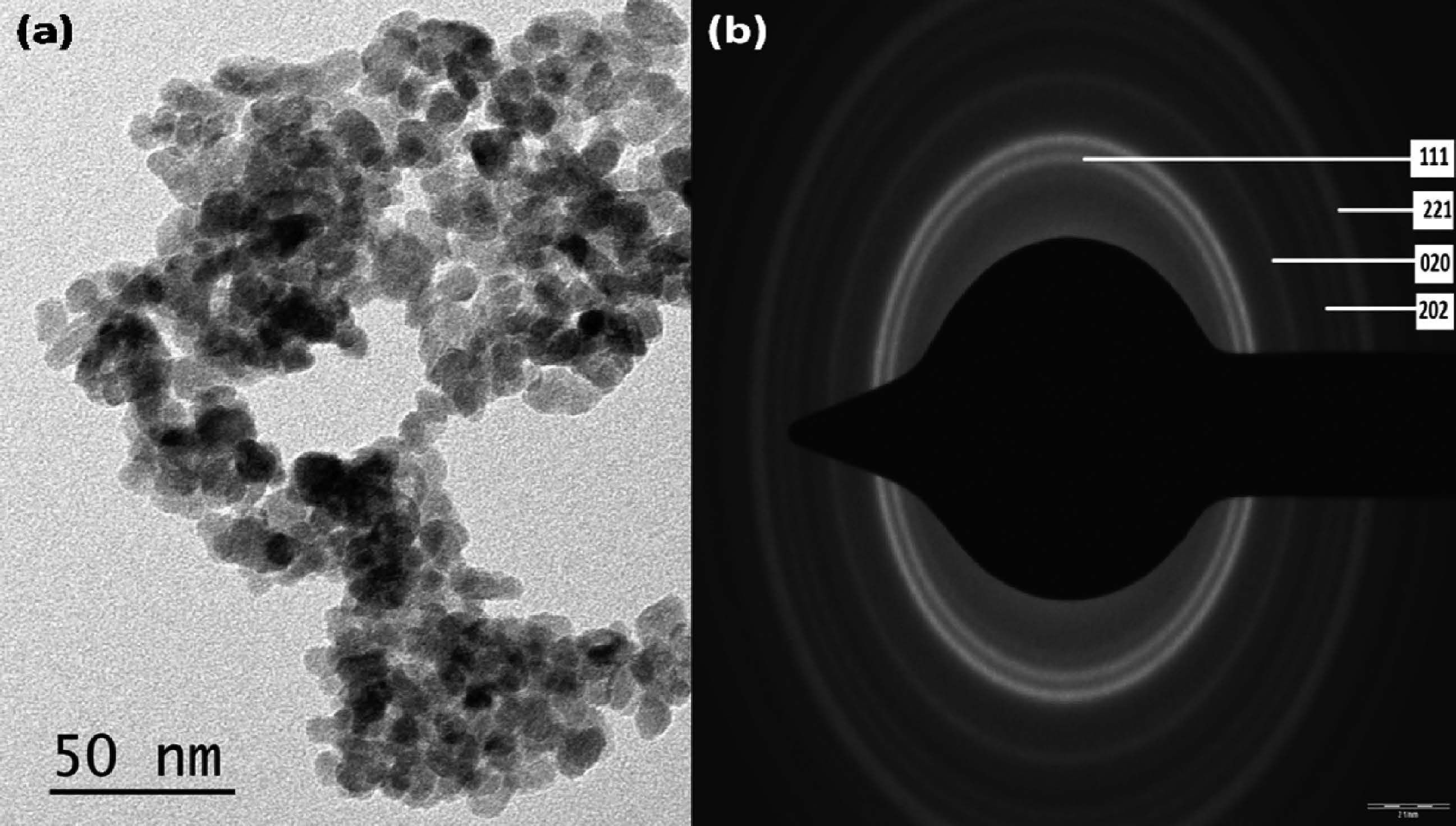
Fig. 1.
(a) TEM image and (b) SAED pattern of CuO nanoparticles.
SEMICONDUCTOR PHYSICS
Jiji Koshy, M. Soosen Samuel, Anoop Chandran and K. C. George
Corresponding author: K. C. George, Email: drkcgeorge@gmail.com
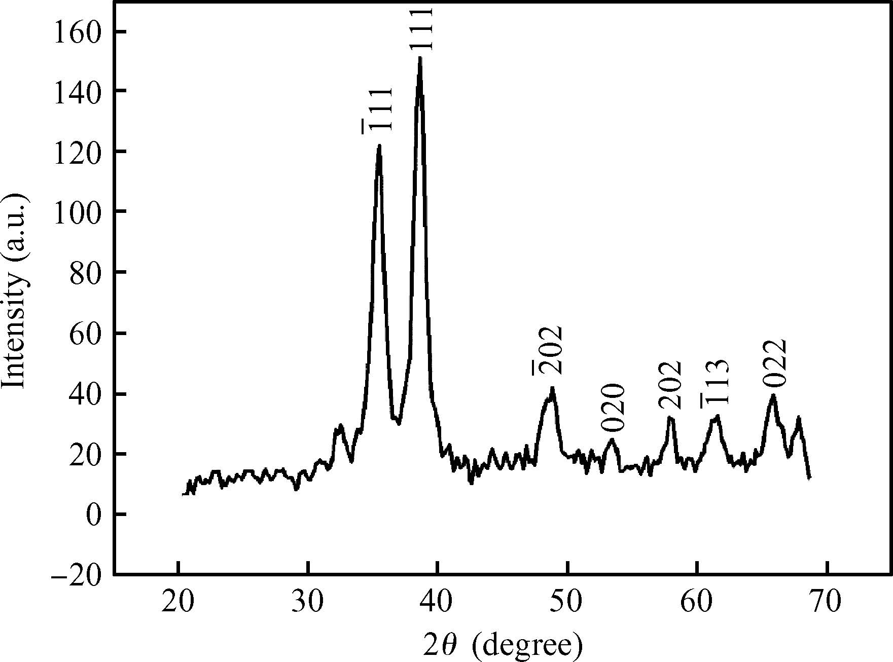
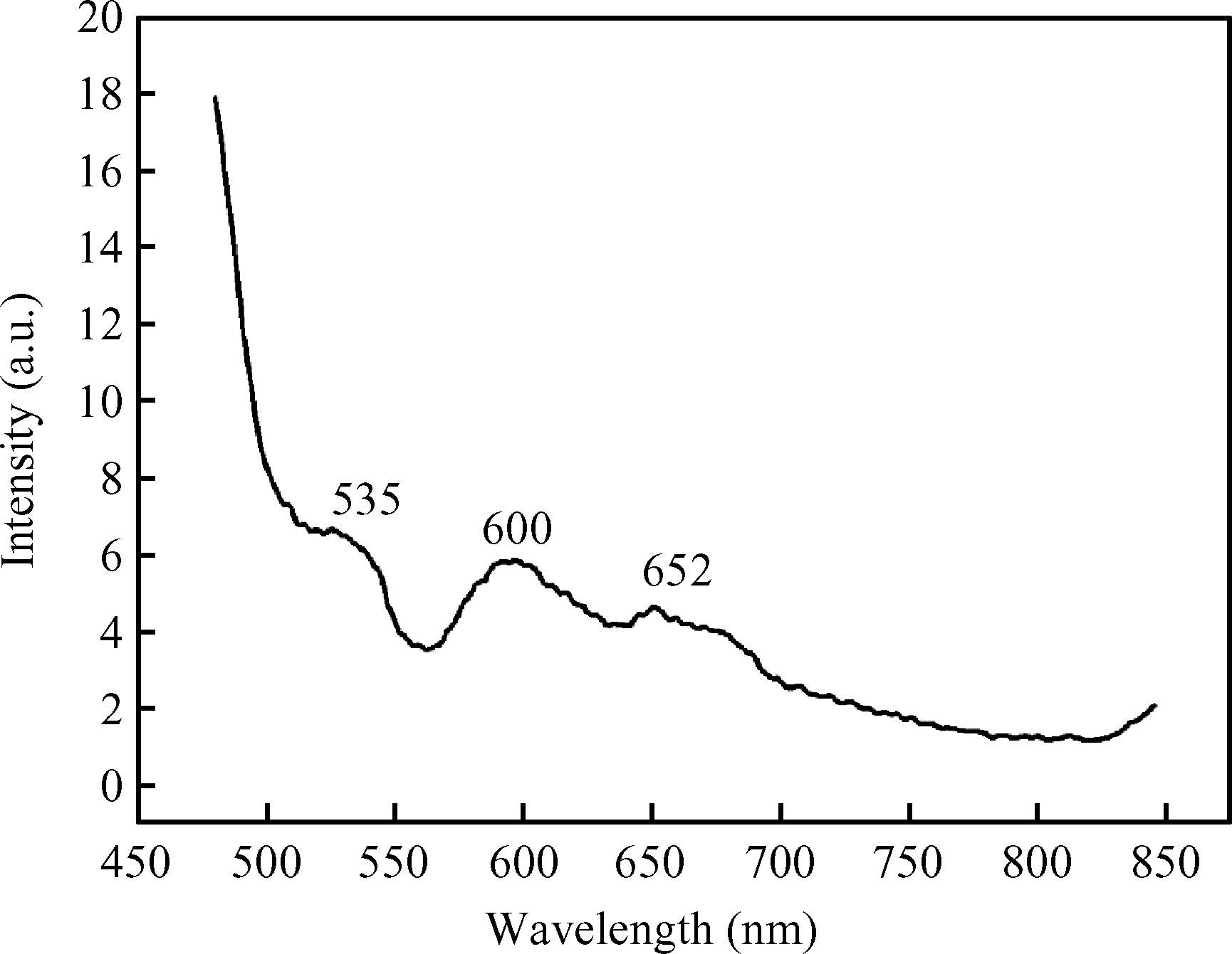
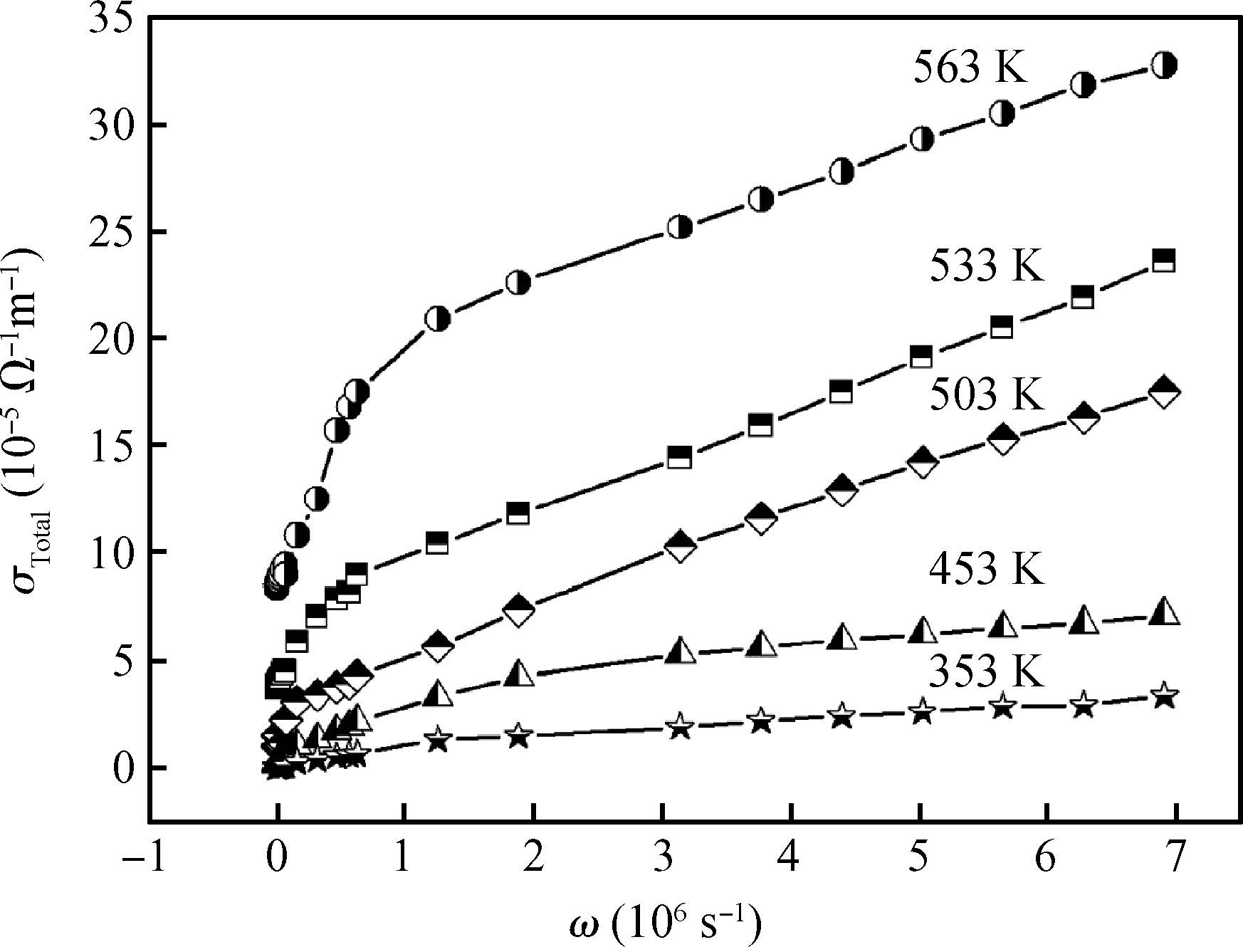
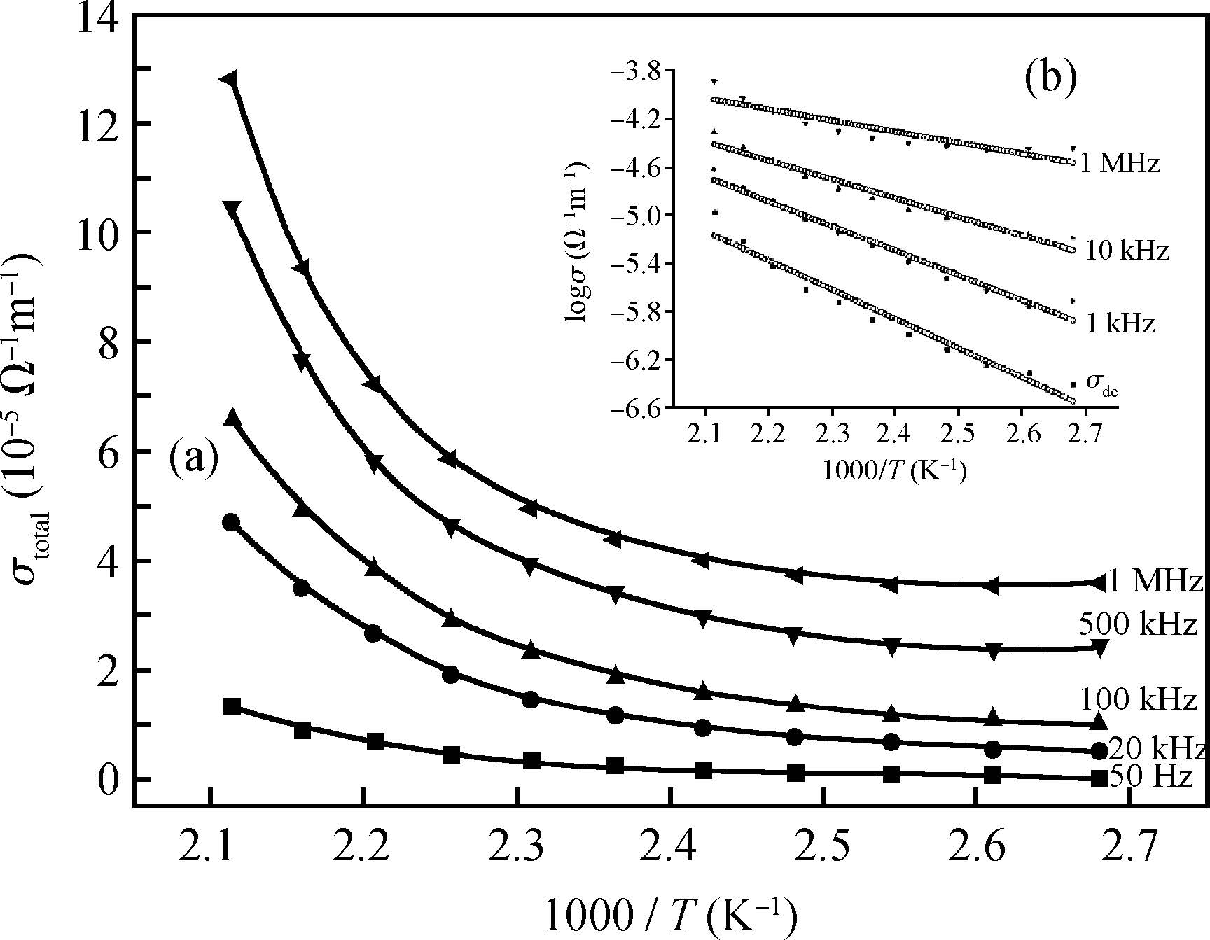
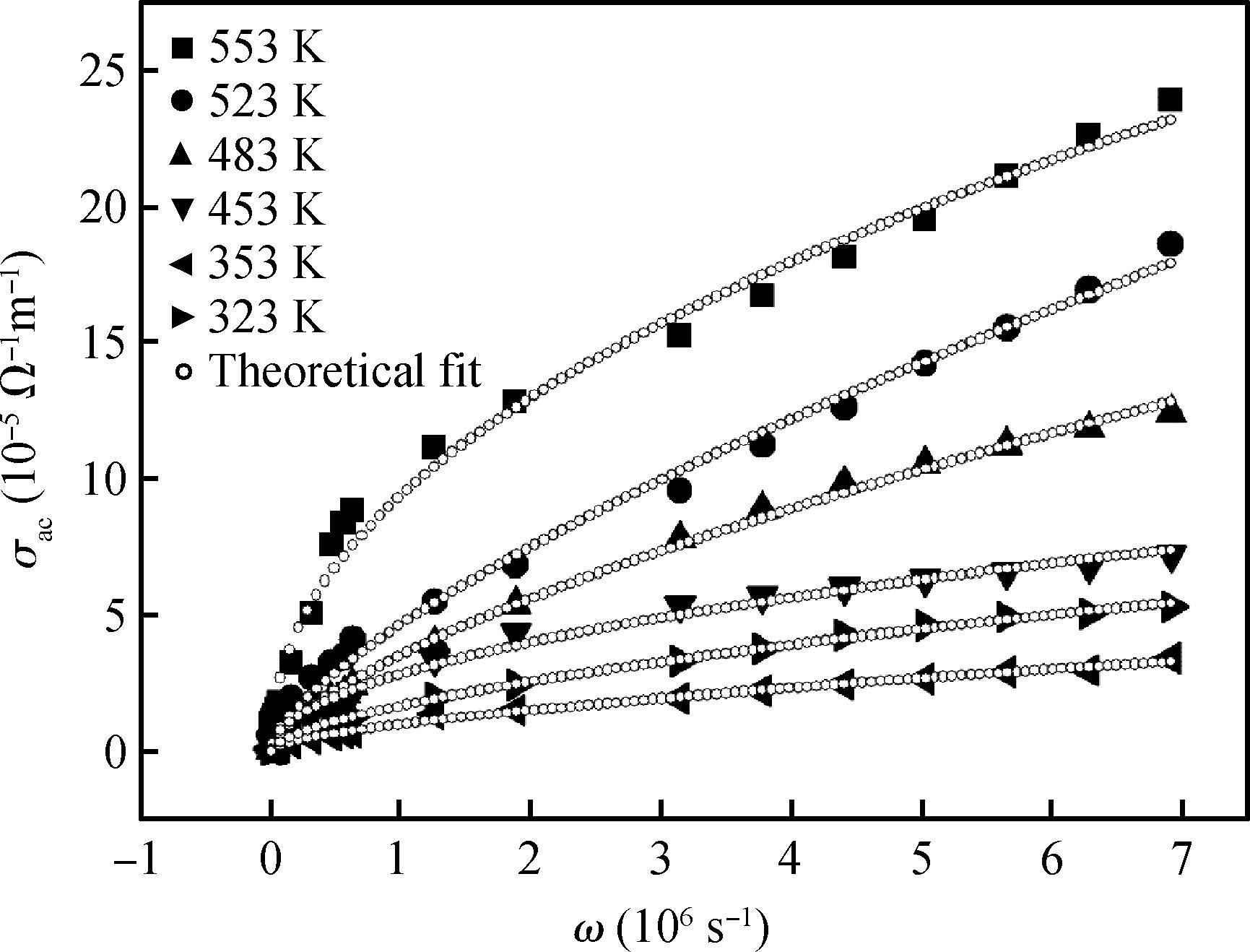
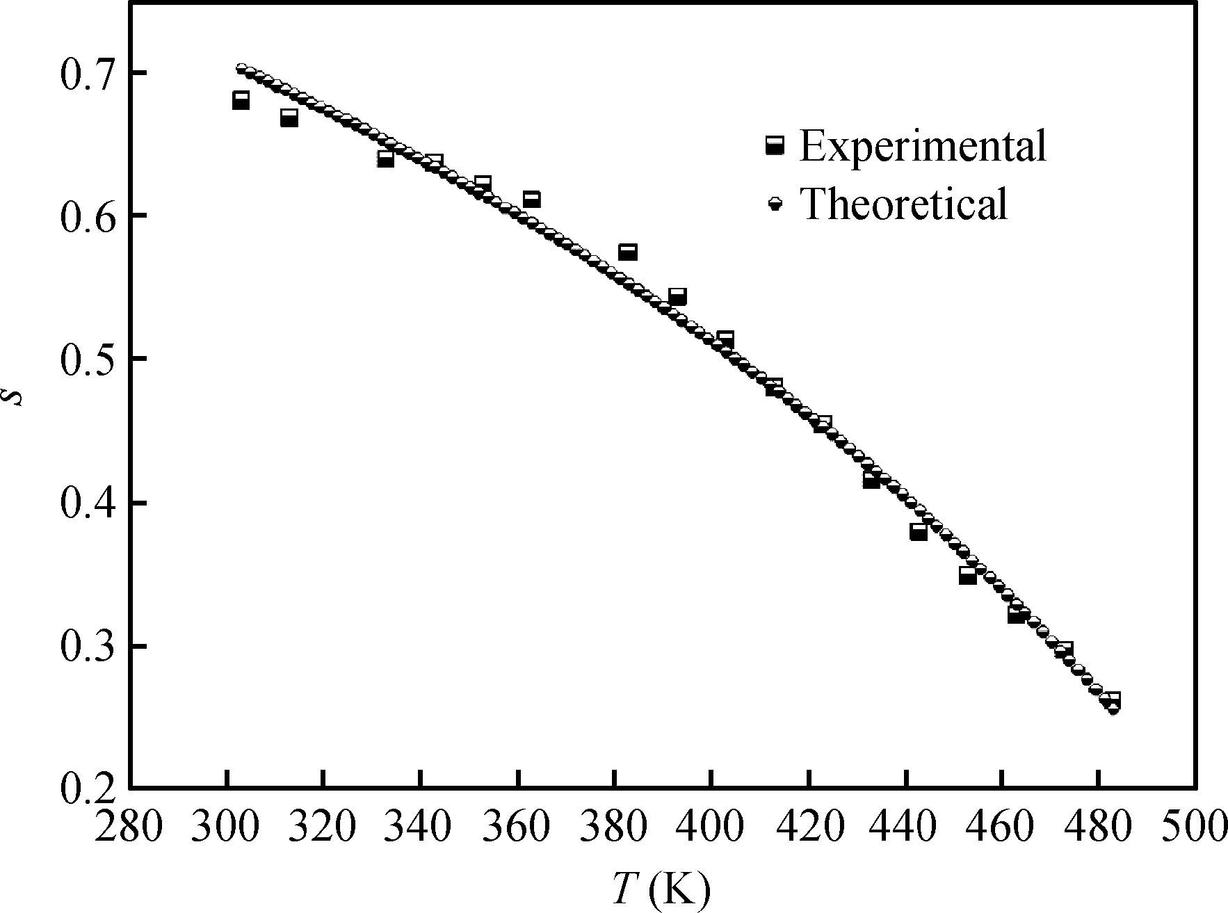
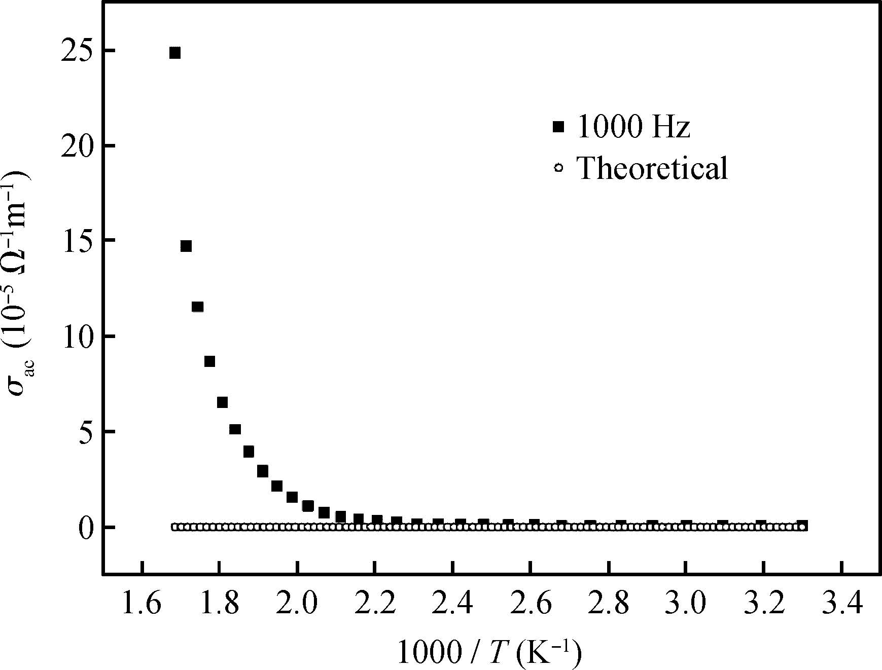
Abstract: The ac conduction mechanism in copper oxide nanoparticles with 8 nm size, synthesized by a precipitation method was studied by analyzing ac conductivity in the frequency range of 50 Hz-1 MHz and in the temperature range of 373-573 K. X-ray diffraction and transmission electron microscopy(TEM) were employed for the structural and morphological characterization of CuO nanoparticles. The experimental and theoretical investigations suggested that the ac conduction mechanism in CuO nanoparticles can be successfully explained by a correlated barrier hopping model, which provided reasonable values for the maximum barrier height and characteristic relaxation time. It was also found that bipolaron hopping become prominent up to a particular temperature and beyond that single polaron hopping predominates. Physical parameters such as hopping distance and density of defect states were also calculated. Photoluminescence studies confirm the presence of a surface defect in CuO nanoparticles.
Key words: CuO nanoparticles, correlated barrier hopping, defect states, photoluminescence spectrum, single polaron hopping
| [1] | |
| [2] | |
| [3] | |
| [4] | |
| [5] | |
| [6] | |
| [7] | |
| [8] | |
| [9] | |
| [10] | |
| [11] | |
| [12] | |
| [13] | |
| [14] | |
| [15] | |
| [16] | |
| [17] | |
| [18] | |
| [19] | |
| [20] | |
| [21] | |
| [22] | |
| [23] | |
| [24] | |
| [25] | |
| [26] | |
| [27] | |
| [28] | |
| [29] |


Article views: 5625 Times PDF downloads: 60 Times Cited by: 0 Times
Received: 10 February 2015 Revised: Online: Published: 01 December 2015
| Citation: |
Jiji Koshy, M. Soosen Samuel, Anoop Chandran, K. C. George. Correlated barrier hopping of CuO nanoparticles[J]. Journal of Semiconductors, 2015, 36(12): 122003. doi: 10.1088/1674-4926/36/12/122003
****
J Koshy,M S. Samuel, A. Chandran, K. C. George. Correlated barrier hopping of CuO nanoparticles[J]. J. Semicond., 2015, 36(12): 122003. doi: 10.1088/1674-4926/36/12/122003.

|
| [1] | |
| [2] | |
| [3] | |
| [4] | |
| [5] | |
| [6] | |
| [7] | |
| [8] | |
| [9] | |
| [10] | |
| [11] | |
| [12] | |
| [13] | |
| [14] | |
| [15] | |
| [16] | |
| [17] | |
| [18] | |
| [19] | |
| [20] | |
| [21] | |
| [22] | |
| [23] | |
| [24] | |
| [25] | |
| [26] | |
| [27] | |
| [28] | |
| [29] |

 WeChat ID
Journal of Semiconductors © 2017 All Rights Reserved 京ICP备05085259号-2

 DownLoad: