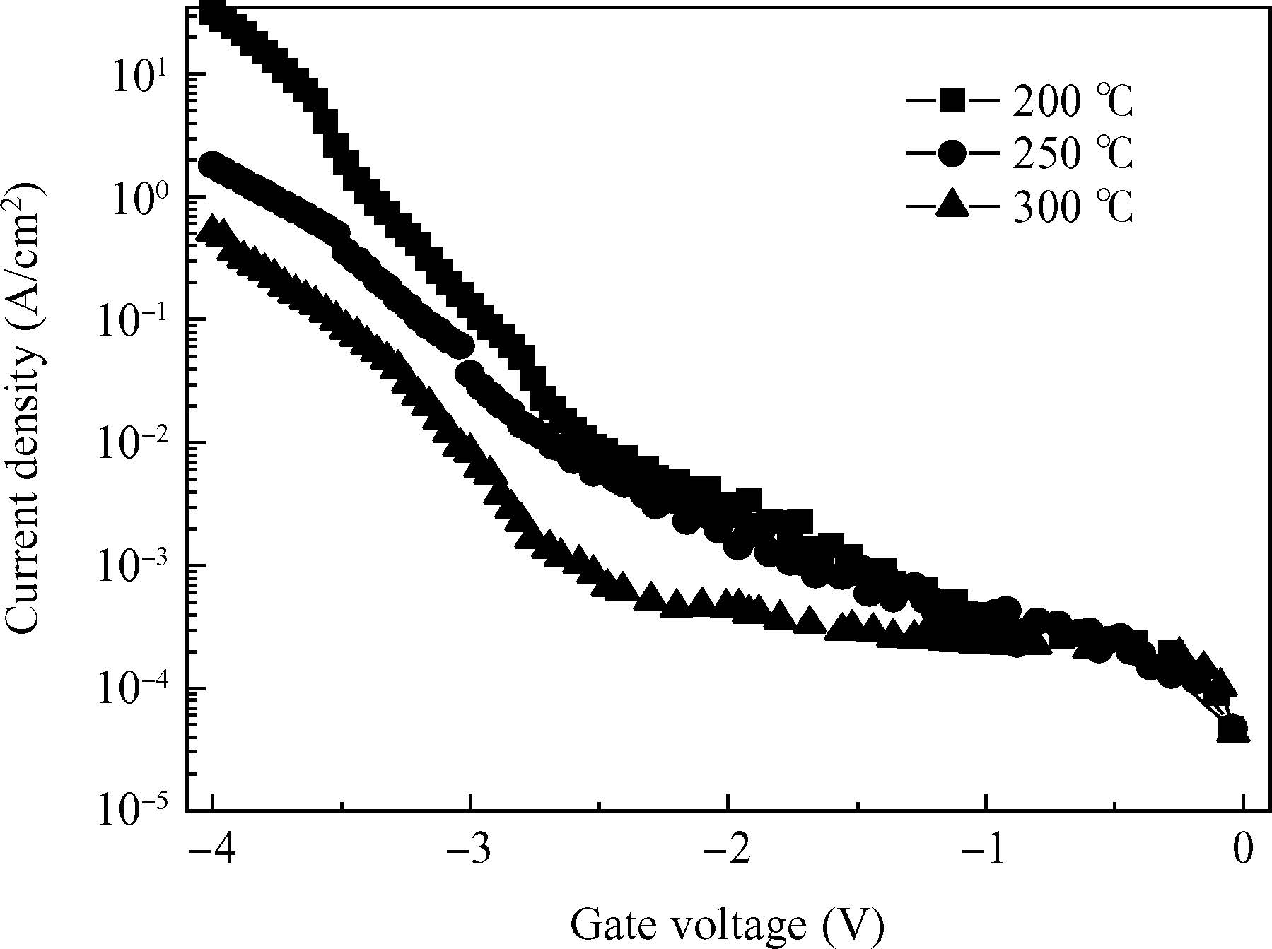
Processing math: 100%
J. Semicond. > 2015, Volume 36 > Issue 12 > 124003

SEMICONDUCTOR DEVICES

Temperature dependent interfacial and electrical characteristics during atomic layer deposition and annealing of HfO2 films in p-GaAs metal-oxide-semiconductor capacitors

Chen Liu, Yuming Zhang, Yimen Zhang, Hongliang Lü and Bin Lu

+ Author Affiliations

 Corresponding author: Lü Hongliang,Email:hllv@mail.xidian.edu.cn

DOI: 10.1088/1674-4926/36/12/124003

PDF

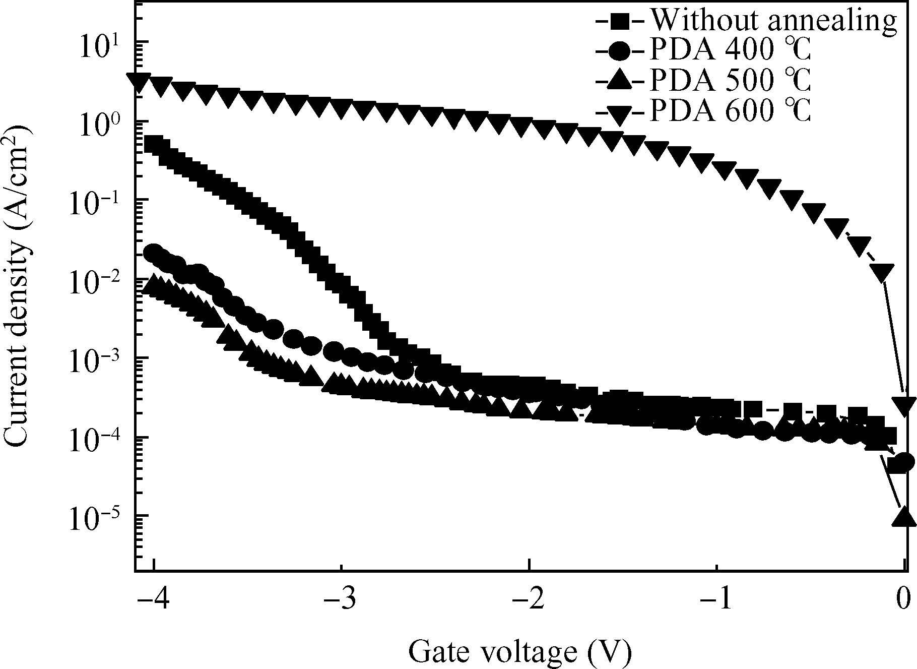
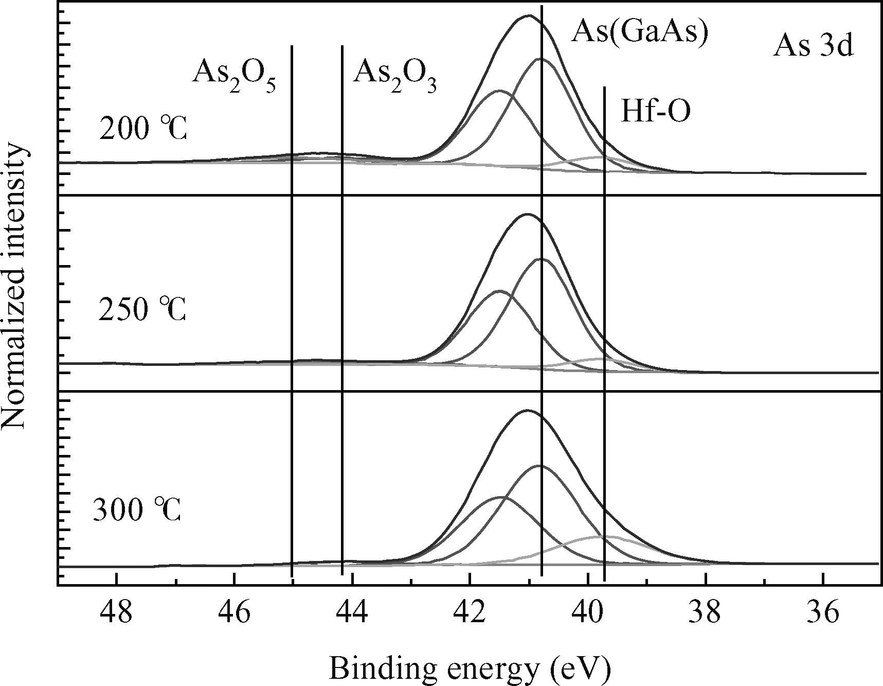
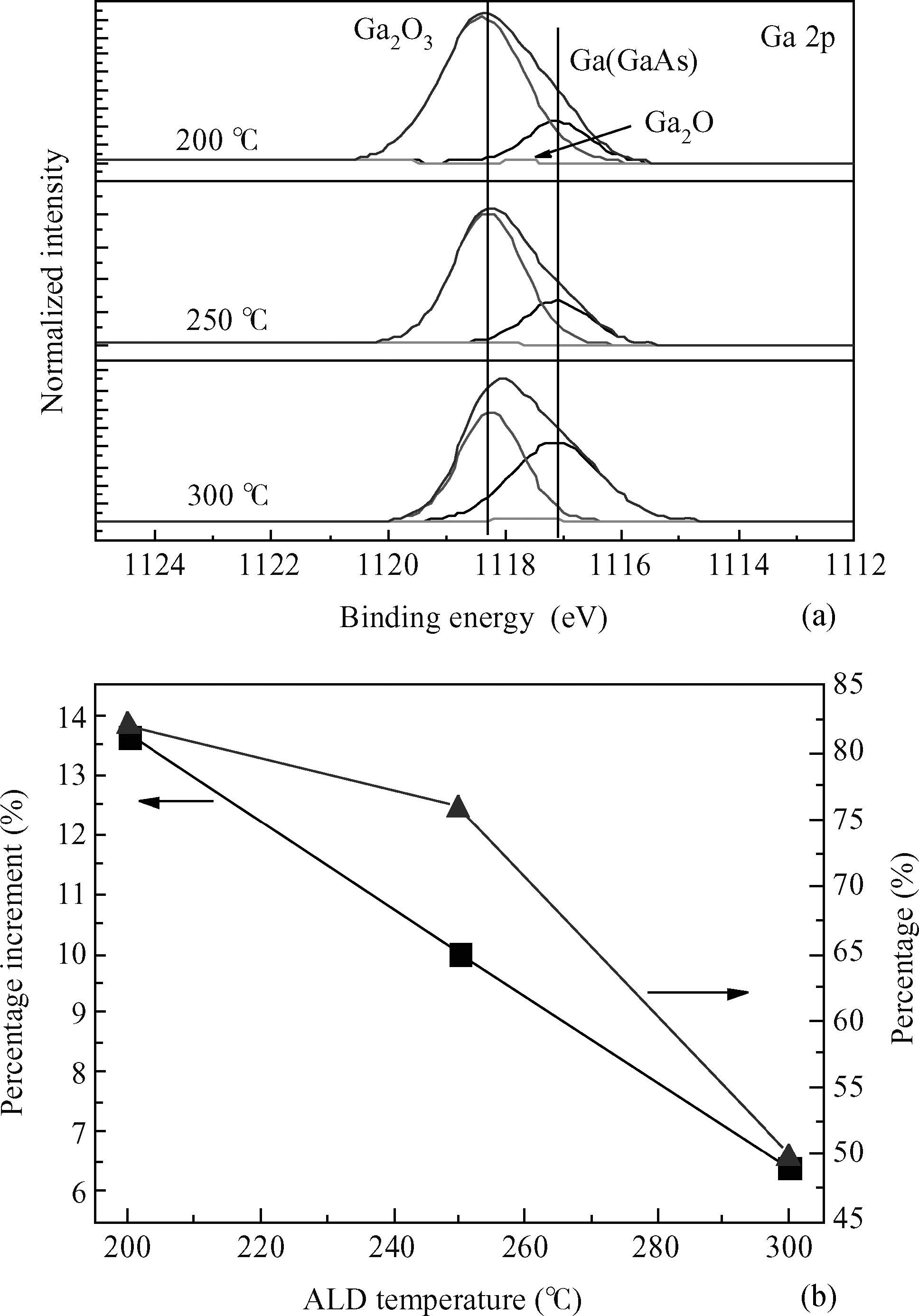
Abstract: We have investigated the temperature dependent interfacial and electrical characteristics of p-GaAs metal-oxide-semiconductor capacitors during atomic layer deposition(ALD) and annealing of HfO2 using the tetrakis(ethylmethyl) amino hafnium precursor. The leakage current decreases with the increase of the ALD temperature and the lowest current is obtained at 300℃ as a result of the Frenkel-Poole conduction induced leakage current being greatly weakened by the reduction of interfacial oxides at the higher temperature. Post deposition annealing(PDA) at 500℃ after ALD at 300℃ leads to the lowest leakage current compared with other annealing temperatures. A pronounced reduction in As oxides during PDA at 500℃ has been observed using X-ray photoelectron spectroscopy at the interface resulting in a proportional increase in Ga2O3. The increment of Ga2O3 after PDA depends on the amount of residual As oxides after ALD. Thus, the ALD temperature plays an important role in determining the high-k/GaAs interface condition. Meanwhile, an optimum PDA temperature is essential for obtaining good dielectric properties.

Key words: GaAs metal-oxide-semiconductor capacitortemperatureinterfaceleakage current

Recently the strong need for ultrahigh-speed logic devices[1, 2, 3] has driven complementary metal-oxide-\break semiconductor (CMOS) researchers to search for alternative substrates including III-V compound semiconductors such as GaAs,InP,and InGaAs due to their high electron mobility,high injection velocity,and low power consumption[4, 5, 6, 7, 8]. However,the most challenging problem for the III-V based metal-oxide-semiconductor field effect transistor (MOSFET) is the Fermi-level pinning[9, 10, 11] due to the large density of defect states within the GaAs band gap opposing the formation of an inversion in the channel. Furthermore,large amounts of native oxides including As oxides (As2O3 and As2O5) and Ga2O3 contribute to high interface trap density (Dit) on GaAs[12, 13, 14],so the removal of interfacial oxides at the high k/GaAs interface is a key factor for achieving high performance MOS transistor operation. Meanwhile,the continuous MOSFET size scaling leads to an inevitably high gate leakage,which limits the maximum drain current and noise margin,thereby severely degrading the flexibility of the circuit design and hindering the CMOS low consumption application[15, 16, 17].

In order to obtain a better interface quality as well as lower gate leakage,we have systematically investigated in this study the role of the temperature during ALD and annealing in determining the interfacial and electrical properties of Al/HfO2/p-GaAs MOS capacitors. Detailed analysis of current-voltage (I-V) measurements has been demonstrated to show the effect of ALD and annealing temperature on the gate dielectric properties. In addition,monochromatic X-ray photoelectron spectroscopy (XPS) has also been used to provide a comprehensive understanding of the temperature controlled reaction at the HfO2/p-GaAs interface.

The GaAs wafers used in this study were single-polished,p-type (100) oriented,Zn-doped with a doping concentration of 5 × 1016 cm3. Prior to deposition,the samples were firstly rinsed using acetone,isopropanol and DI water,then soaked in HCl for 1 min for native oxide removal,and finally dipped in (NH4)2S (10%) for 1 min to passivate elemental As[18]. Then the pre-treated substrates were loaded inside the ALD chamber for HfO2 dielectric deposition using TEMAH (Hf precursor) and H2O (oxygen precursor). The growth temperature was set as 200,250,and 300 ℃,respectively. The ALD process has been discussed in detail in the previous paper[19]. The physical thickness of HfO2 was measured to be 3.1 nm by Sopra GES5E spectroscopic ellipsometry. Then the post deposition annealing (PDA) process was carried out by rapid thermal annealing (RTA) at 400,500,and 600 ℃ for 1 min under N2 ambient. Control samples without PDA were also fabricated. Finally,a MOS capacitor structure was produced by fabricating an Al gate electrode using the lift-off method followed by e-beam evaporating Ti (20 nm)/Au (150 nm) metal stack as the backside ohmic contact. The e-beam evaporated Al electrode was a circle with an area of 5.8 × 103 cm2 and a thickness of 200~nm. The chemical structure of the interface between HfO2 and p-GaAs was analyzed by XPS using a monochromatic Al Kα X-ray source (1486.7 eV) with a line width of 0.25 eV and a take-off angle (TOA) of 45[20,21]. The XPS spectra were compensated with a C 1s binding energy of 284.8 eV and then carefully deconvoluted using the Avantage software[22]. All XPS fits included a Shirley background subtraction and kept the full width half maximum (FWHM) of specific core-level features unchanged[23]. The HP 4156B semiconductor parameter analyzer was used for I-V characterizations.

According to our results published in the previous paper,it can be concluded that better interface quality can be achieved at a higher ALD temperature[19]. In addition,a more intensive study on the relationship between dielectric leakage properties and ALD temperature will be discussed in the following.

Figure1 illustrates the I-V characteristics of p-GaAs MOS capacitors with HfO2 deposited at different ALD temperatures without annealing. The leakage current decreases with the increase of ALD temperature and the lowest leakage current is obtained at 300 ℃. From the previous XPS analysis,it can be concluded that the lowest amount of interfacial oxides is achieved at the interface for 300 ℃ resulting in the lowest Dit. However,there are large amounts of Ga-O and As-O bonds for 200 and 250 ℃[19]. So,the Frenkel-Poole emission dominates the leakage current because of the bad interface between HfO2 and GaAs at a lower ALD temperature[24,\,25]. However,the Frenkel-Poole conduction diminishes greatly and leads to the evident reduction of gate leakage current for ALD at 300~℃ because of the interface improvement due to the enhanced "self-cleaning" effect[26]. The Schottky emission mechanism presumably dominates in this case as the GaAs/HfO2 barrier height is just 1.47 eV[27]. In general,the difference of leakage current with ALD temperature is consistent with the previous capacitance-voltage (C-V) measurements and XPS result[19].

Figure  1.  I-V characteristics of Al/HfO2/p-GaAs MOS capacitors for different ALD temperatures without annealing.

Figure2 shows the I-V characteristics after annealing HfO2 layer with different PDA temperatures for ALD at 300℃. It can be observed that the lowest leakage current is obtained for 500℃ annealing. Up to 500 ℃,the densification effect of the HfO2 dielectric dominates and improves the dielectric properties[28]. So,the leakage current decreases until 500℃. However,high temperature annealing above 500~℃ results in the crystallization of the high-k dielectric,which produces grain boundaries that serve as high leakage paths in the gate oxide[29]. Moreover,annealing at 600 ℃ accelerates the diffusion of Ga and As elements into the HfO2 layer,severely degrading the dielectric properties thus lead to a jump in leakage current[28]. The I-V measurements clearly show that 500℃ is the optimum PDA temperature to obtain good dielectric properties. In the following,a further study will be performed using XPS on the reaction chemistry of interfacial oxides for samples annealing at 500℃ after different temperatures of ALD.

Figure  2.  I-V characteristics after annealing HfO2 on p-GaAs with different PDA temperatures for ALD at 300 ℃.

Figure3 shows As 3d spectra for HfO2 deposited on GaAs and subjected to a (500℃,1 min) PDA. The peaks due to arsenic oxides,As2O5 and As2O3,are at binding energies of 45.0 and 44.2 eV,respectively,while the doublet peak at 40.8 eV is assigned as As-Ga bonding taking into account the spin-orbit splitting using an intensity ratio of 3 : 2 and a separation of 0.69~eV[30]. It is interesting to observe that for an ALD temperature of 200,250,or 300 ℃,residual arsenic oxides[19] decrease evidently after annealing at 500 ℃,and for 300 ℃ treated samples,almost no arsenic oxides are detected. This suggests that the residual arsenic oxides after ALD are consumed during PDA.

Figure  3.  As 3d core-level spectra of GaAs after annealing HfO2 at 500 ℃ for different ALD temperatures.

On the contrary,the Ga 2p3/2 spectra shows a proportional increase in the Ga2O3 peak at a binding energy of 1118.26 eV[31] compared with control samples[19] after annealing as indicated in Figure4. The amount of Ga2O3 is detected in the smart mode of the Avantage software as 82.07%,75.90%,and 49.84%,respectively after annealing and the corresponding increment compared with control samples[19] is 13.66%,10.03%,and 6.39%,respectively for ALD temperatures of 200 ℃,250 ℃,and 300 ℃,respectively as shown in Figure4(b). It can be concluded that more Ga2O3 after PDA is closely related to the consumption of As oxides via an exchange reaction in which As oxides react with the GaAs substrate and convert to Ga2O3 as shown in Equation (1)[32]:

Figure  4.  XPS Ga 2p3/2 spectra analysis of GaAs after annealing HfO2 at 500 \du for different ALD temperatures. (a) Ga 2p3/2 core-level spectra. (b) Plot of the percentage and percentage increment of Ga2O3 after annealing versus ALD temperature.

Thus,an insignificant reduction of As oxides during ALD at 200 ℃ results in more Ga2O3 at the interface after PDA,while an obvious reduction during ALD at 300 ℃ leads to the least Ga2O3 formation after PDA.

In summary,we have studied the temperature dependent characteristics during ALD and annealing in Al/HfO2/p-GaAs MOS capacitors using TEMAH as the precursor. The leakage current for ALD at 300 ℃ is the lowest,as the Frenkel-Poole emission which dominates the leakage current in the presence of a large amount of defect states is greatly weakened due to the improvement of the interface quality at a higher temperature. I-V measurements also indicate that 500 ℃ is the optimum PDA temperature to obtain the lowest leakage current compared with other annealing temperatures. Meanwhile,annealing of HfO2 at 500 ℃ decomposes the residual As2O3 after ALD and forms Ga2O3 via an exchange reaction. It is reasonable to conclude that ALD growth of HfO2 at 300 ℃ using the TEMAH precursor followed by annealing at 500 ℃ provides a feasible way to obtain a good high-k/GaAs interface as well as preferable dielectric properties suitable for future III-V MOS applications.

The authors would like to acknowledge the contributions of Professor ZHANG David Wei in Fudan University and Mr. FANG Run-Chen in Arizona State University for their ALD deposition work.


[1]
[2]
[3]
[4]
[5]
[6]
[7]
[8]
[9]
[10]
[11]
[12]
[13]
[14]
[15]
[16]
[17]
[18]
[19]
[20]
[21]
[22]
[23]
[24]
[25]
[26]
[27]
[28]
[29]
[30]
[31]
[32]
Fig. 1.  I-V characteristics of Al/HfO2/p-GaAs MOS capacitors for different ALD temperatures without annealing.

Fig. 2.  I-V characteristics after annealing HfO2 on p-GaAs with different PDA temperatures for ALD at 300 ℃.

Fig. 3.  As 3d core-level spectra of GaAs after annealing HfO2 at 500 ℃ for different ALD temperatures.

Fig. 4.  XPS Ga 2p3/2 spectra analysis of GaAs after annealing HfO2 at 500 \du for different ALD temperatures. (a) Ga 2p3/2 core-level spectra. (b) Plot of the percentage and percentage increment of Ga2O3 after annealing versus ALD temperature.

[1]
[2]
[3]
[4]
[5]
[6]
[7]
[8]
[9]
[10]
[11]
[12]
[13]
[14]
[15]
[16]
[17]
[18]
[19]
[20]
[21]
[22]
[23]
[24]
[25]
[26]
[27]
[28]
[29]
[30]
[31]
[32]
1

Characterization of interfaces: Lessons from the past for the future of perovskite solar cells

Wanlong Wang, Dongyang Zhang, Rong Liu, Deepak Thrithamarassery Gangadharan, Furui Tan, et al.

Journal of Semiconductors, 2022, 43(5): 051202. doi: 10.1088/1674-4926/43/5/051202

2

Fabrication of room temperature continuous-wave operation GaN-based ultraviolet laser diodes

Degang Zhao, Jing Yang, Zongshun Liu, Ping Chen, Jianjun Zhu, et al.

Journal of Semiconductors, 2017, 38(5): 051001. doi: 10.1088/1674-4926/38/5/051001

3

A simple chemical route to synthesize the umangite phase of copper selenide (Cu3Se2) thin film at room temperature

Balasaheb M. Palve, Sandesh R. Jadkar, Habib M. Pathan

Journal of Semiconductors, 2017, 38(6): 063003. doi: 10.1088/1674-4926/38/6/063003

4

Characterization of the effects of nitrogen and hydrogen passivation on SiO2/4H-SiC interface by low temperature conductance measurements

Yiyu Wang, Zhaoyang Peng, Huajun Shen, Chengzhan Li, Jia Wu, et al.

Journal of Semiconductors, 2016, 37(2): 026001. doi: 10.1088/1674-4926/37/2/026001

5

Effect of ultrasound on reverse leakage current of silicon Schottky barrier structure

O.Ya Olikh, K.V. Voitenko, R.M. Burbelo, JaM. Olikh

Journal of Semiconductors, 2016, 37(12): 122002. doi: 10.1088/1674-4926/37/12/122002

6

Progress in complementary metal-oxide-semiconductor silicon photonics and optoelectronic integrated circuits

Hongda Chen, Zan Zhang, Beiju Huang, Luhong Mao, Zanyun Zhang, et al.

Journal of Semiconductors, 2015, 36(12): 121001. doi: 10.1088/1674-4926/36/12/121001

7

Inhomogeneous barrier height effect on the current-voltage characteristics of an Au/n-InP Schottky diode

Kamal Zeghdar, Lakhdar Dehimi, Achour Saadoune, Nouredine Sengouga

Journal of Semiconductors, 2015, 36(12): 124002. doi: 10.1088/1674-4926/36/12/124002

8

Electro-magnetic weak coupling optical polaron and temperature effect in quantum dot

M. Tiotsop, A. J. Fotue, S. C. Kenfack, N. Issofa, A. V. Wirngo, et al.

Journal of Semiconductors, 2015, 36(10): 102001. doi: 10.1088/1674-4926/36/10/102001

9

Comparative study of leakage power in CNTFET over MOSFET device

Sanjeet Kumar Sinha, Saurabh Chaudhury

Journal of Semiconductors, 2014, 35(11): 114002. doi: 10.1088/1674-4926/35/11/114002

10

Fluorine-plasma surface treatment for gate forward leakage current reduction in AlGaN/GaN HEMTs

Wanjun Chen, Jing Zhang, Bo Zhang, Kevin Jing Chen

Journal of Semiconductors, 2013, 34(2): 024003. doi: 10.1088/1674-4926/34/2/024003

11

Physical properties of spray deposited CdTe thin films: PEC performance

V. M. Nikale, S. S. Shinde, C. H. Bhosale, K.Y. Rajpure

Journal of Semiconductors, 2011, 32(3): 033001. doi: 10.1088/1674-4926/32/3/033001

12

A 2.2-V 2.9-ppm/℃ BiCMOS bandgap voltage reference with full temperature-range curvature-compensation

Zhou Zekun, Ma Yingqian, Ming Xin, Zhang Bo, Li Zhaoji, et al.

Journal of Semiconductors, 2010, 31(7): 075004. doi: 10.1088/1674-4926/31/7/075004

13

Theoretical study of the SiO2/Si interface and its effect on energy band profile and MOSFET gate tunneling current

Zhu Huiwen, Liu Yongsong, Mao Lingfeng, Shen Jingqin, Zhu Zhiyan, et al.

Journal of Semiconductors, 2010, 31(8): 082003. doi: 10.1088/1674-4926/31/8/082003

14

Accurate and fast table look-up models for leakage current analysis in 65 nm CMOS technology

Xue Jiying, Li Tao, Yu Zhiping

Journal of Semiconductors, 2009, 30(2): 024004. doi: 10.1088/1674-4926/30/2/024004

15

Temperature effects on interface polarons in a strained (111)-oriented zinc-blende GaN/AlGaN heterojunction under pressure

Zhang Min, Ban Shiliang

Journal of Semiconductors, 2009, 30(3): 032001. doi: 10.1088/1674-4926/30/3/032001

16

Temperature and Process Variations Aware Dual Threshold Voltage Footed Domino Circuits Leakage Management

Gong Na, Wang Jinhui, Guo Baozeng, Pang Jiao

Journal of Semiconductors, 2008, 29(12): 2364-2371.

17

Temperature Distribution in Ridge Structure InGaN Laser Diodes and Its Influence on Device Characteristics

Li Deyao, Huang Yongzhen, Zhang Shuming, Chong Ming, Ye Xiaojun, et al.

Chinese Journal of Semiconductors , 2006, 27(3): 499-505.

18

Alloy Temperature Dependence of Offset Voltage and Ohmic Contact Resistance in Thin Base InGaP/GaAs HBTs

Yang Wei, Liu Xunchun, Zhu Min, Wang Runmei, Shen Huajun, et al.

Chinese Journal of Semiconductors , 2006, 27(5): 765-768.

19

Numerical Simulation and Analysis of SiGeC/Si Heterojunction Power Diodes

Gao Yong, Liu Jing, Ma Li, Yu Mingbin

Chinese Journal of Semiconductors , 2006, 27(6): 1068-1072.

20

Temperature Dependence of Vacuum Rabi Splitting in a Single Quantum Dot-Semiconductor Microcavity

Zhu Kadi, Li Waisang

Chinese Journal of Semiconductors , 2006, 27(3): 489-493.

  • Search

    Advanced Search >>

    GET CITATION

    Chen Liu, Yuming Zhang, Yimen Zhang, Hongliang Lü, Bin Lu. Temperature dependent interfacial and electrical characteristics during atomic layer deposition and annealing of HfO2 films in p-GaAs metal-oxide-semiconductor capacitors[J]. Journal of Semiconductors, 2015, 36(12): 124003. doi: 10.1088/1674-4926/36/12/124003
    C Liu, Y M Zhang, Y M Zhang, H Lü, B Lu. Temperature dependent interfacial and electrical characteristics during atomic layer deposition and annealing of HfO2 films in p-GaAs metal-oxide-semiconductor capacitors[J]. J. Semicond., 2015, 36(12): 124003. doi: 10.1088/1674-4926/36/12/124003.
    shu

    Export: BibTex EndNote

    Article Metrics

    Article views: 2785 Times PDF downloads: 32 Times Cited by: 0 Times

    History

    Received: 26 April 2015 Revised: Online: Published: 01 December 2015

    Catalog

      Email This Article

      User name:
      Email:*请输入正确邮箱
      Code:*验证码错误
      Chen Liu, Yuming Zhang, Yimen Zhang, Hongliang Lü, Bin Lu. Temperature dependent interfacial and electrical characteristics during atomic layer deposition and annealing of HfO2 films in p-GaAs metal-oxide-semiconductor capacitors[J]. Journal of Semiconductors, 2015, 36(12): 124003. doi: 10.1088/1674-4926/36/12/124003 ****C Liu, Y M Zhang, Y M Zhang, H Lü, B Lu. Temperature dependent interfacial and electrical characteristics during atomic layer deposition and annealing of HfO2 films in p-GaAs metal-oxide-semiconductor capacitors[J]. J. Semicond., 2015, 36(12): 124003. doi: 10.1088/1674-4926/36/12/124003.
      Citation:
      Chen Liu, Yuming Zhang, Yimen Zhang, Hongliang Lü, Bin Lu. Temperature dependent interfacial and electrical characteristics during atomic layer deposition and annealing of HfO2 films in p-GaAs metal-oxide-semiconductor capacitors[J]. Journal of Semiconductors, 2015, 36(12): 124003. doi: 10.1088/1674-4926/36/12/124003 ****
      C Liu, Y M Zhang, Y M Zhang, H Lü, B Lu. Temperature dependent interfacial and electrical characteristics during atomic layer deposition and annealing of HfO2 films in p-GaAs metal-oxide-semiconductor capacitors[J]. J. Semicond., 2015, 36(12): 124003. doi: 10.1088/1674-4926/36/12/124003.

      Temperature dependent interfacial and electrical characteristics during atomic layer deposition and annealing of HfO2 films in p-GaAs metal-oxide-semiconductor capacitors

      DOI: 10.1088/1674-4926/36/12/124003
      Funds:

      Project supported by the Advance Research Project of China(No. 5130803XXXX) and the National Natural Science Foundation of China(No. 61176070).

      More Information
      • Corresponding author: Lü Hongliang,Email:hllv@mail.xidian.edu.cn
      • Received Date: 2015-04-26
      • Accepted Date: 2015-06-17
      • Published Date: 2015-01-25

      Catalog

        /

        DownLoad:  Full-Size Img  PowerPoint
        Return
        Return