Fig1.
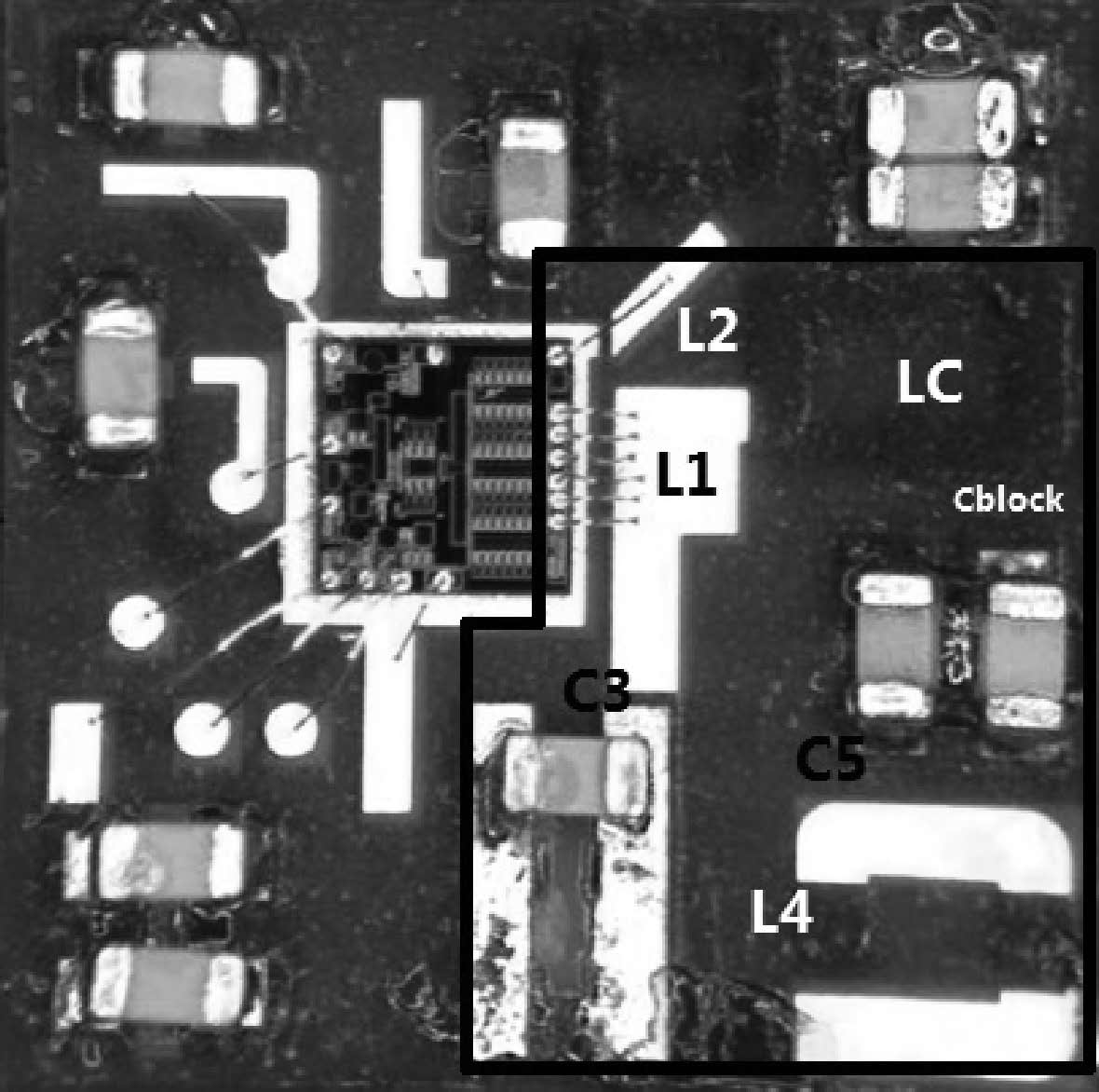
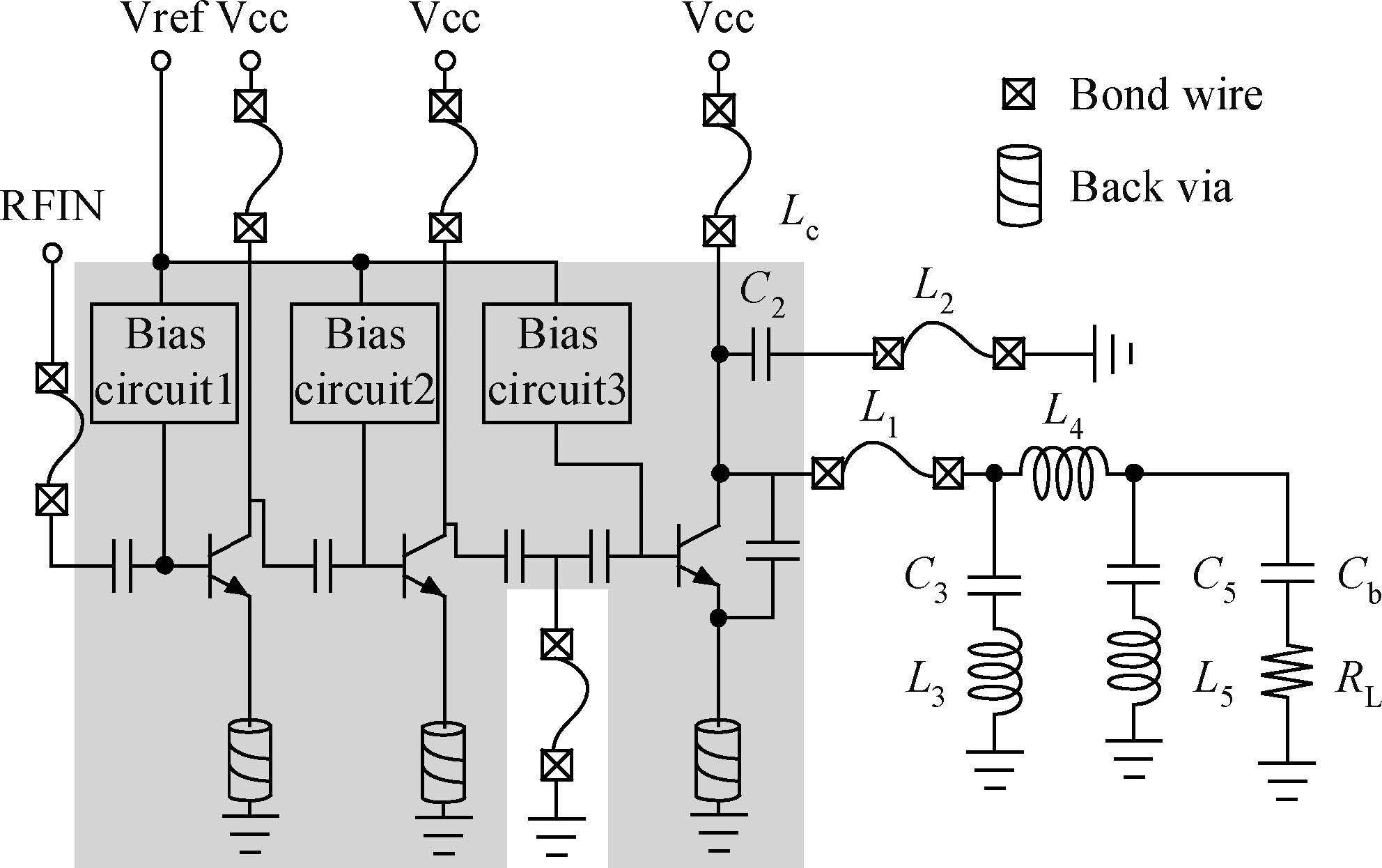
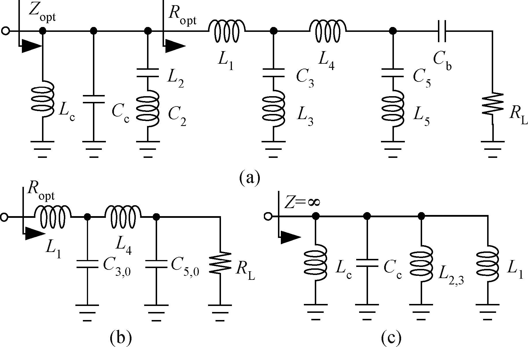
Configuration of class-F PA with output matching circuit.
SEMICONDUCTOR INTEGRATED CIRCUITS
Junming Lin, Guohao Zhang, Yaohua Zheng, Sizhen Li, Zhihao Zhang and Sidi Chen
Corresponding author: Lin Junming,Email:junminglin@yeah.net
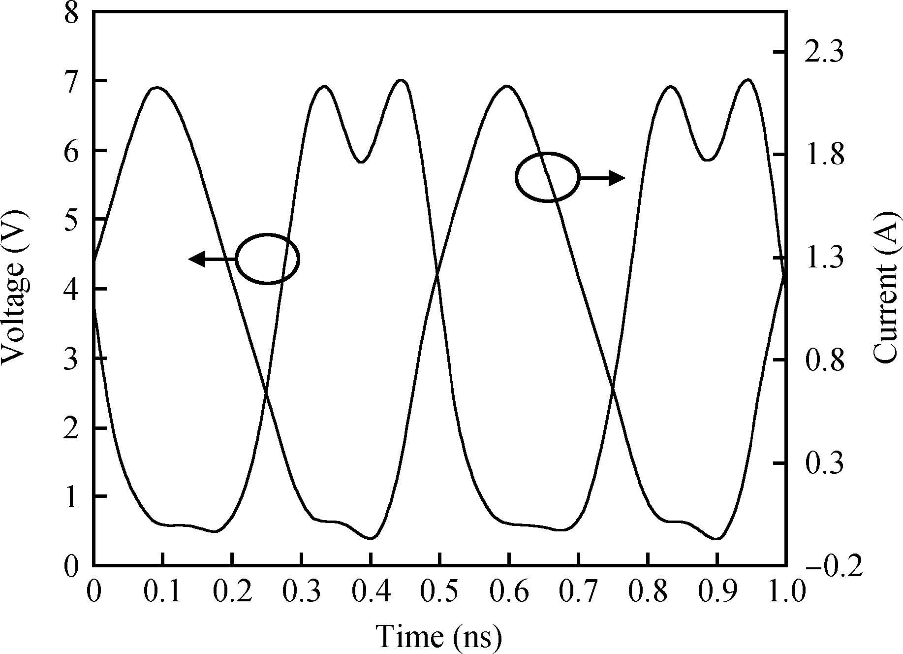
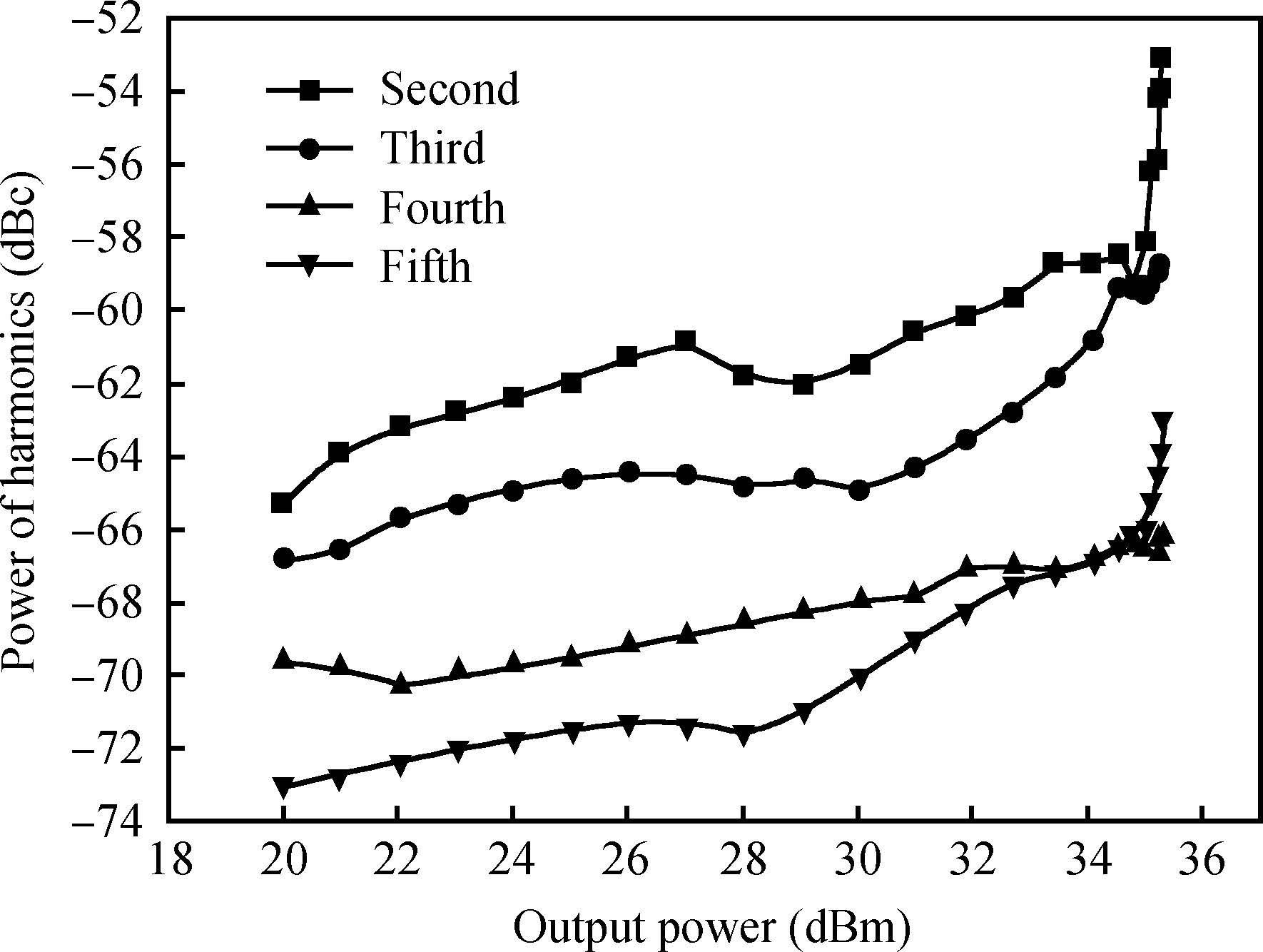
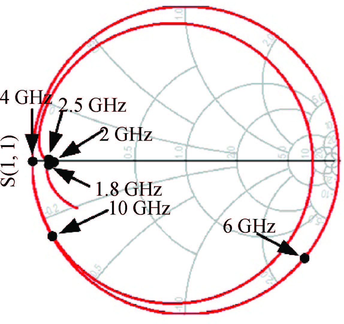
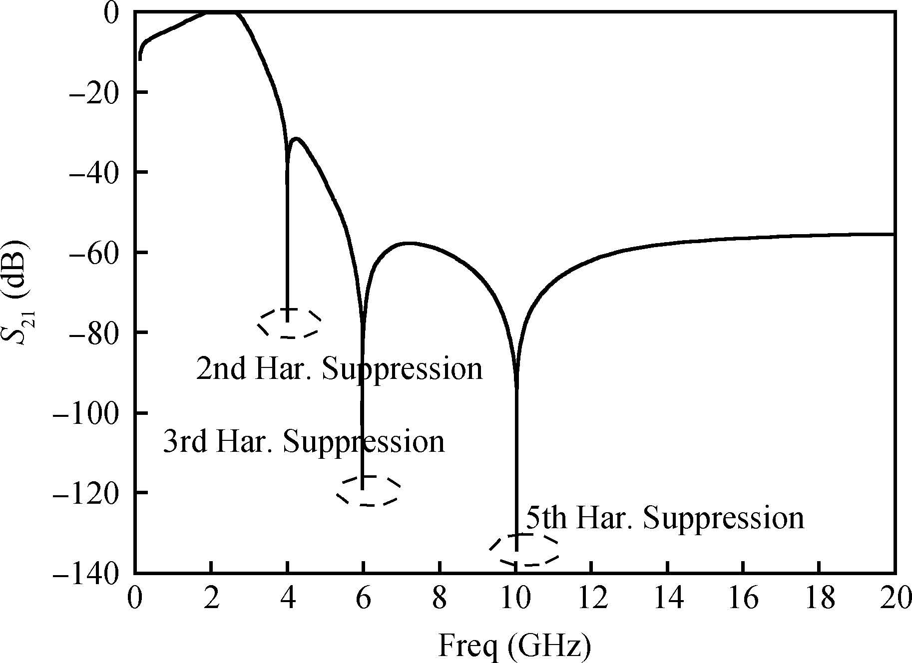
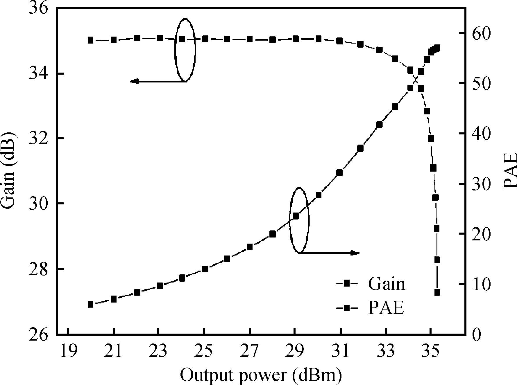
Abstract: A broadband class-F power amplifier for an S-band handset device is integrated on a 3×3×0.82 mm3 die using an InGaP/GaAs HBT process. With LC serial harmonic traps immersed into the broadband output matching circuit, good harmonic suppression performance can be achieved. A pure resistive impedance of the matching circuit, but near zero at second and infinite at third harmonic frequency, which enhances the efficiency, is obtained across 1.8-2.5 GHz. Tested with a continuous wave(CW) signal, the PA delivers an output power of 34 dBm and achieves a PAE of 57% at 2 GHz. In addition, excellent harmonic suppression levels of less than-53 dBc across the second to fifth harmonic are obtained.
Key words: S-band, power amplifier, broadband, class-F, harmonic suppression, InGaP/GaAs HBT
| [1] | |
| [2] | |
| [3] | |
| [4] | |
| [5] | |
| [6] | |
| [7] | |
| [8] | |
| [9] | |
| [10] | |
| [11] | |
| [12] | |
| [13] | |
| [14] |
| [1] | |
| [2] | |
| [3] | |
| [4] | |
| [5] | |
| [6] | |
| [7] | |
| [8] | |
| [9] | |
| [10] | |
| [11] | |
| [12] | |
| [13] | |
| [14] |


Article views: 3875 Times PDF downloads: 41 Times Cited by: 0 Times
Received: 26 March 2015 Revised: Online: Published: 01 December 2015
| Citation: |
Junming Lin, Guohao Zhang, Yaohua Zheng, Sizhen Li, Zhihao Zhang, Sidi Chen. Design of broadband class-F power amplifier with high-order harmonic suppression for S-band application[J]. Journal of Semiconductors, 2015, 36(12): 125002. doi: 10.1088/1674-4926/36/12/125002
****
J M Lin, G H Zhang, Y H Zheng, S Z Li, Z H Zhang, S D Chen. Design of broadband class-F power amplifier with high-order harmonic suppression for S-band application[J]. J. Semicond., 2015, 36(12): 125002. doi: 10.1088/1674-4926/36/12/125002.

|
| [1] | |
| [2] | |
| [3] | |
| [4] | |
| [5] | |
| [6] | |
| [7] | |
| [8] | |
| [9] | |
| [10] | |
| [11] | |
| [12] | |
| [13] | |
| [14] |

 WeChat ID
Journal of Semiconductors © 2017 All Rights Reserved 京ICP备05085259号-2

 DownLoad: