


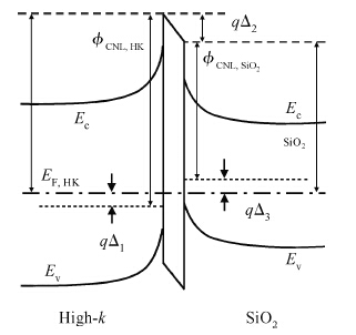
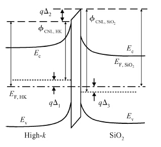
Fig. 1.
A schematic diagram of the energy band structure for a negative dipole formation in a high-$k$/SiO$_{2}$ system.
SEMICONDUCTOR TECHNOLOGY
Kai Han1, , Xiaolei Wang2, Hong Yang2 and Wenwu Wang2
Corresponding author: Kai Han, E-mail: hankai@wfu.edu.cn
Abstract: The formation of an electric dipole at the high-k/SiO2 interface is quantitatively analyzed. The band lineups and physical origin of dipole formation at the high-k/SiO2 interface are explained by the dielectric contact induced gap states (DCIGS). The charge neutrality level (CNL) of the DCIGS, which represents a distribution of high-k and SiO2 contact induced gap states, is utilized to study the dipole moment. The charge transfer due to different CNLs of high-k and SiO2 is considered as the dominant origin of dipole formation. The theoretically calculated dipole strengths of high-k/SiO2 systems based on this model are in good agreement with the experimental data.
Keywords: high-k dielectric, band alignment, interface dipole
| [1] | |
| [2] | |
| [3] | |
| [4] | |
| [5] | |
| [6] | |
| [7] | |
| [8] | |
| [9] | |
| [10] | |
| [11] | |
| [12] | |
| [13] | |
| [14] | |
| [15] | |
| [16] | |
| [17] | |
| [18] | |
| [19] | |
| [20] | |
| [21] | |
| [22] | |
| [23] | |
| [24] |
| [1] | |
| [2] | |
| [3] | |
| [4] | |
| [5] | |
| [6] | |
| [7] | |
| [8] | |
| [9] | |
| [10] | |
| [11] | |
| [12] | |
| [13] | |
| [14] | |
| [15] | |
| [16] | |
| [17] | |
| [18] | |
| [19] | |
| [20] | |
| [21] | |
| [22] | |
| [23] | |
| [24] |


Article views: 4020 Times PDF downloads: 99 Times Cited by: 0 Times
Received: 19 August 2014 Revised: Online: Published: 01 March 2015
| Citation: |
Kai Han, Xiaolei Wang, Hong Yang, Wenwu Wang. Electric dipole formation at high-k dielectric/SiO2 interface[J]. Journal of Semiconductors, 2015, 36(3): 036004. doi: 10.1088/1674-4926/36/3/036004
****
K Han, X L Wang, H Yang, W W Wang. Electric dipole formation at high-k dielectric/SiO2 interface[J]. J. Semicond., 2015, 36(3): 036004. doi: 10.1088/1674-4926/36/3/036004.

|
| [1] | |
| [2] | |
| [3] | |
| [4] | |
| [5] | |
| [6] | |
| [7] | |
| [8] | |
| [9] | |
| [10] | |
| [11] | |
| [12] | |
| [13] | |
| [14] | |
| [15] | |
| [16] | |
| [17] | |
| [18] | |
| [19] | |
| [20] | |
| [21] | |
| [22] | |
| [23] | |
| [24] |

 WeChat ID
Journal of Semiconductors © 2017 All Rights Reserved 京ICP备05085259号-2

 DownLoad:

