


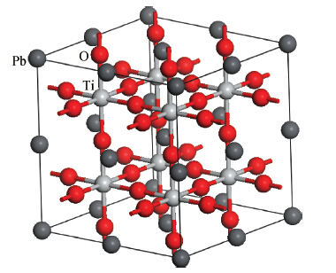
Fig. 1.
(Color online) The 2 $\times $ 2 $\times $ 2 supercell of the cubic perovskite PbTiO$_{3}$. The black, gray, and red spheres represent Pb, Ti, and O atoms, respectively.
SEMICONDUCTOR MATERIALS
Peijiang Niu, Jinliang Yan and Delan Meng
Corresponding author: Jinliang Yan, E-mail: yanjinliang8@sina.com
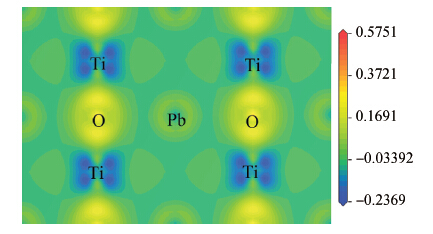
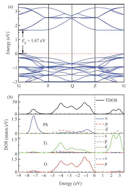
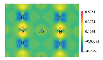
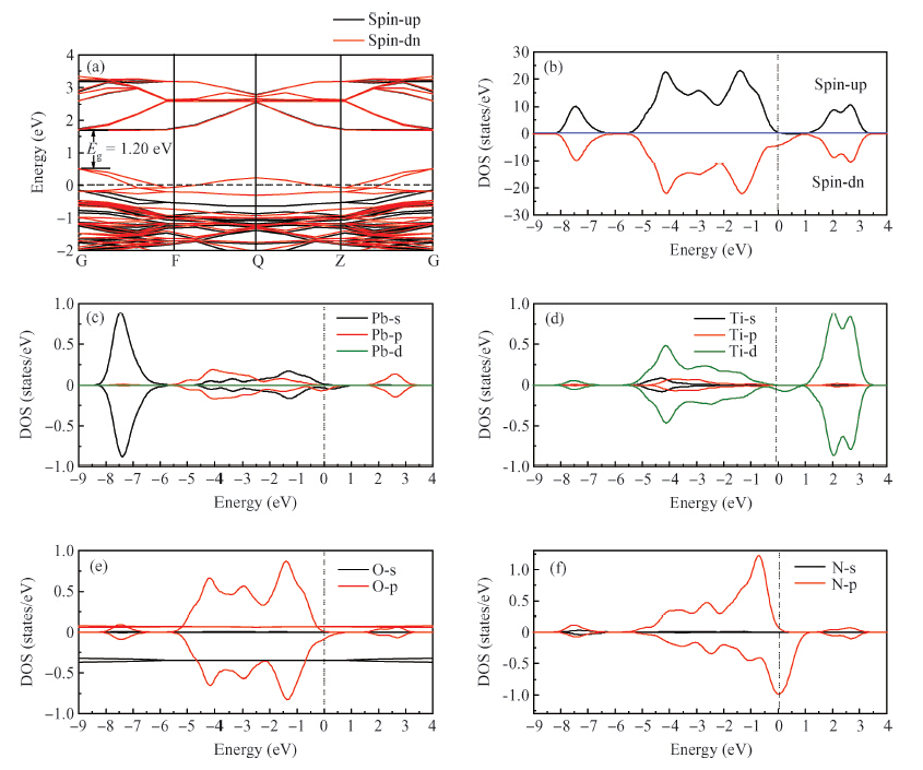
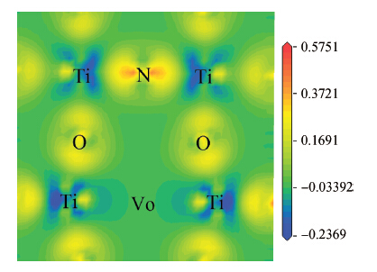
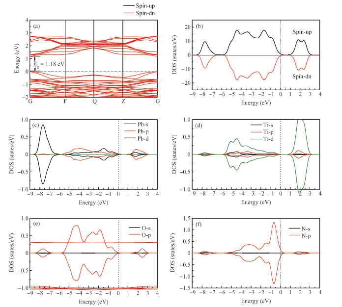
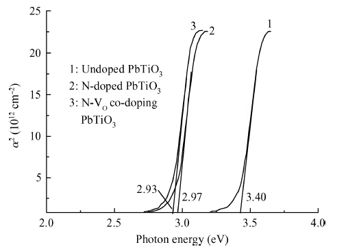
Abstract: By using spin-polarized density functional theory calculations, the electron density differences, band structures and density of states of p-type N-doped PbTiO3 have been studied. In addition, the oxygen vacancy in N-doped PbTiO3 is also discussed. After the nitrogen dopant is introduced into the crystal, the N-doped PbTiO3 system is spin-polarized, the spin-down valance bands move to a high energy level and the Fermi energy level moves to the top of the valance bands, finally the band gap is narrowed. In this process, the N-doped PbTiO3 shows typical p-type semiconductor characteristics. When an oxygen vacancy and N impurity coexist in PbTiO3, there is no spin-polarized phenomenon. The conduction bands move downward and the acceptors are found to be fully compensated. The calculation results are mostly consistent with the experimental data.
Keywords: semiconductor doping, electric properties, optical band gaps, optical properties, lead titanate
| [1] | |
| [2] | |
| [3] | |
| [4] | |
| [5] | |
| [6] | |
| [7] | |
| [8] | |
| [9] | |
| [10] | |
| [11] | |
| [12] | |
| [13] | |
| [14] | |
| [15] | |
| [16] | |
| [17] | |
| [18] | |
| [19] | |
| [20] | |
| [21] | |
| [22] | |
| [23] |
| [1] | |
| [2] | |
| [3] | |
| [4] | |
| [5] | |
| [6] | |
| [7] | |
| [8] | |
| [9] | |
| [10] | |
| [11] | |
| [12] | |
| [13] | |
| [14] | |
| [15] | |
| [16] | |
| [17] | |
| [18] | |
| [19] | |
| [20] | |
| [21] | |
| [22] | |
| [23] |


Article views: 3110 Times PDF downloads: 24 Times Cited by: 0 Times
Received: 02 September 2014 Revised: Online: Published: 01 April 2015
| Citation: |
Peijiang Niu, Jinliang Yan, Delan Meng. The effects of N-doping and oxygen vacancy on the electronic structure and conductivity of PbTiO3[J]. Journal of Semiconductors, 2015, 36(4): 043004. doi: 10.1088/1674-4926/36/4/043004
****
P J Niu, J L Yan, D L Meng. The effects of N-doping and oxygen vacancy on the electronic structure and conductivity of PbTiO3[J]. J. Semicond., 2015, 36(4): 043004. doi: 10.1088/1674-4926/36/4/043004.

|
| [1] | |
| [2] | |
| [3] | |
| [4] | |
| [5] | |
| [6] | |
| [7] | |
| [8] | |
| [9] | |
| [10] | |
| [11] | |
| [12] | |
| [13] | |
| [14] | |
| [15] | |
| [16] | |
| [17] | |
| [18] | |
| [19] | |
| [20] | |
| [21] | |
| [22] | |
| [23] |

 WeChat ID
Journal of Semiconductors © 2017 All Rights Reserved 京ICP备05085259号-2

 DownLoad:

