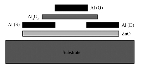
J. Semicond. > 2015, Volume 36 > Issue 4 > 044002

SEMICONDUCTOR DEVICES

Top gate ZnO-Al2O3 thin film transistors fabricated using a chemical bath deposition technique

Paragjyoti Gogoi, Rajib Saikia and Sanjib Changmai

+ Author Affiliations

 Corresponding author: Paragjyoti Gogoi, E-mail: paragjyoti_g@rediffmail.com

DOI: 10.1088/1674-4926/36/4/044002

PDF

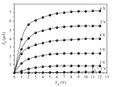
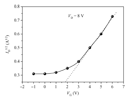
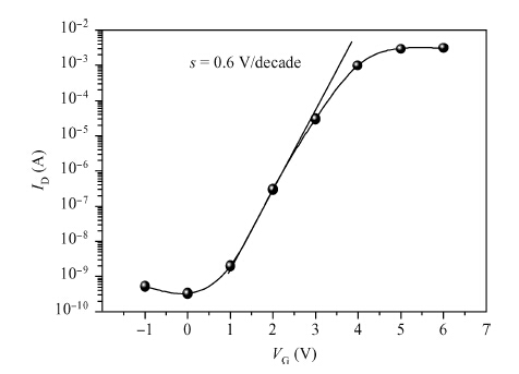
Abstract: ZnO thin films were prepared by a simple chemical bath deposition technique using an inorganic solution mixture of ZnCl2 and NH3 on glass substrates and then were used as the active material in thin film transistors (TFTs). The TFTs were fabricated in a top gate coplanar electrode structure with high-k Al2O3 as the gate insulator and Al as the source, drain and gate electrodes. The TFTs were annealed in air at 500 ℃ for 1 h. The TFTs with a 50 μm channel length exhibited a high field-effect mobility of 0.45 cm2/(V·s) and a low threshold voltage of 1.8 V. The sub-threshold swing and drain current ON-OFF ratio were found to be 0.6 V/dec and 106, respectively.

Key words: chemical bath depositionthin film transistorselectrical properties


[1]
[2]
[3]
[4]
[5]
[6]
[7]
[8]
[9]
[10]
[11]
[12]
[13]
[14]
[15]
[16]
[17]
[18]
[19]
[20]
[21]
Fig. 1.  The schematic structure of the top gate coplanar electrode structure of the TFTs.

Fig. 2.  XRD spectrum of the ZnO thin film.

Fig. 3.  An SEM image of the ZnO thin film annealed at 500 C.

Fig. 4.  $I_{\rm D}$-$V_{\rm D}$ characteristics of the ZnO TFTs at constant $V_{\rm G}$.

Fig. 5.  $I_{\rm D}^{1/2}$ -$V_{\rm G}$ plots for ZnO TFTs at a constant drain voltage $V_{\rm D}$ $=$ 8 V.

Fig. 6.  Plot of lg $I_{\rm D}$-$V_{\rm G}$ at a constant drain voltage $V_{\rm D}$ $=$ 8 V.

DownLoad: CSV
DownLoad: CSV

Table 1.   Measured values of mobility ($\mu_{\rm FET})$, threshold voltage ($V_{\rm T})$, ON-OFF ratio and sub-threshold swing of the fabricated devices and comparison of these parameters with some previous results[1, 3, 4] with different gate dielectrics and methods of preparation.

DownLoad: CSV
[1]
[2]
[3]
[4]
[5]
[6]
[7]
[8]
[9]
[10]
[11]
[12]
[13]
[14]
[15]
[16]
[17]
[18]
[19]
[20]
[21]
1

Structural and optical studies on PVA capped SnS films grown by chemical bath deposition for solar cell application

P Mallika Bramaramba Devi, G. Phaneendra Reddy, K. T. Ramakrishna Reddy

Journal of Semiconductors, 2019, 40(5): 052101. doi: 10.1088/1674-4926/40/5/052101

2

Review of recent progresses on flexible oxide semiconductor thin film transistors based on atomic layer deposition processes

Jiazhen Sheng, Ki-Lim Han, TaeHyun Hong, Wan-Ho Choi, Jin-Seong Park, et al.

Journal of Semiconductors, 2018, 39(1): 011008. doi: 10.1088/1674-4926/39/1/011008

3

Oxide-based thin film transistors for flexible electronics

Yongli He, Xiangyu Wang, Ya Gao, Yahui Hou, Qing Wan, et al.

Journal of Semiconductors, 2018, 39(1): 011005. doi: 10.1088/1674-4926/39/1/011005

4

Substrate temperature dependent studies on properties of chemical spray pyrolysis deposited CdS thin films for solar cell applications

Kiran Diwate, Amit Pawbake, Sachin Rondiya, Rupali Kulkarni, Ravi Waykar, et al.

Journal of Semiconductors, 2017, 38(2): 023001. doi: 10.1088/1674-4926/38/2/023001

5

Electrical transport and current properties of rare-earth dysprosium Schottky electrode on p-type GaN at various annealing temperatures

G. Nagaraju, K. Ravindranatha Reddy, V. Rajagopal Reddy

Journal of Semiconductors, 2017, 38(11): 114001. doi: 10.1088/1674-4926/38/11/114001

6

SnS thin films deposited by chemical bath deposition, dip coating and SILAR techniques

Sunil H. Chaki, Mahesh D. Chaudhary, M. P. Deshpande

Journal of Semiconductors, 2016, 37(5): 053001. doi: 10.1088/1674-4926/37/5/053001

7

Structural and opto-electrical properties of pyrolized ZnO-CdO crystalline thin films

A. M. M. Tanveer Karim, M. K. R. Khan, M. Mozibur Rahman

Journal of Semiconductors, 2015, 36(5): 053001. doi: 10.1088/1674-4926/36/5/053001

8

Structural, optical and electrical properties of zinc oxide thin films deposited by a spray pyrolysis technique

Yacine Aoun, Boubaker Benhaoua, Brahim Gasmi, Said Benramache

Journal of Semiconductors, 2015, 36(1): 013002. doi: 10.1088/1674-4926/36/1/013002

9

Electrical properties of Ge:Ga near the metal-insulator transition

M Errai, A El Kaaouachi, H El Idrissi

Journal of Semiconductors, 2015, 36(6): 062001. doi: 10.1088/1674-4926/36/6/062001

10

Effect of Co doping on structural, optical, electrical and thermal properties of nanostructured ZnO thin films

Sonet Kumar Saha, M. Azizar Rahman, M. R. H. Sarkar, M. Shahjahan, M. K. R. Khan, et al.

Journal of Semiconductors, 2015, 36(3): 033004. doi: 10.1088/1674-4926/36/3/033004

11

Effects of interface trap density on the electrical performance of amorphous InSnZnO thin-film transistor

Yongye Liang, Kyungsoo Jang, S. Velumani, Cam Phu Thi Nguyen, Junsin Yi, et al.

Journal of Semiconductors, 2015, 36(2): 024007. doi: 10.1088/1674-4926/36/2/024007

12

Effect of band gap energy on the electrical conductivity in doped ZnO thin film

Said Benramache, Okba Belahssen, Hachemi Ben Temam

Journal of Semiconductors, 2014, 35(7): 073001. doi: 10.1088/1674-4926/35/7/073001

13

Photoconductivity and surface chemical analysis of ZnO thin films deposited by solution-processing techniques for nano and microstructure fabrication

V.K. Dwivedi, P. Srivastava, G. Vijaya Prakash

Journal of Semiconductors, 2013, 34(3): 033001. doi: 10.1088/1674-4926/34/3/033001

14

Correlation between electrical conductivity-optical band gap energy and precursor molarities ultrasonic spray deposition of ZnO thin films

Said Benramache, Okba Belahssen, Abderrazak Guettaf, Ali Arif

Journal of Semiconductors, 2013, 34(11): 113001. doi: 10.1088/1674-4926/34/11/113001

15

Effect of rhenium doping on various physical properties of single crystals of MoSe2

Mihir M. Vora, Aditya M. Vora

Journal of Semiconductors, 2012, 33(1): 012001. doi: 10.1088/1674-4926/33/1/012001

16

Optical and electrical properties of porous silicon layer formed on the textured surface by electrochemical etching

Ou Weiying, Zhao Lei, Diao Hongwei, Zhang Jun, Wang Wenjing, et al.

Journal of Semiconductors, 2011, 32(5): 056002. doi: 10.1088/1674-4926/32/5/056002

17

Optical and electrical properties of electrochemically deposited polyaniline-CeO2 hybrid nanocomposite film

Anees A. Ansari, M. A. M. Khan, M. Naziruddin Khan, Salman A. Alrokayan, M. Alhoshan, et al.

Journal of Semiconductors, 2011, 32(4): 043001. doi: 10.1088/1674-4926/32/4/043001

18

Growth and electrical properties of high-quality Mg-doped p-type Al0.2Ga0.8N films

Zhou Xiaowei, Li Peixian, Xu Shengrui, Hao Yue

Journal of Semiconductors, 2009, 30(4): 043002. doi: 10.1088/1674-4926/30/4/043002

19

NTC and electrical properties of nickel and gold doped n-type silicon material

Dong Maojin, Chen Zhaoyang, Fan Yanwei, Wang Junhua, Tao Mingde, et al.

Journal of Semiconductors, 2009, 30(8): 083007. doi: 10.1088/1674-4926/30/8/083007

20

Optical and electrical properties of N-doped ZnO and fabrication of thin-film transistors

Zhu Xiaming, Wu Huizhen, Wang Shuangjiang, Zhang Yingying, Cai Chunfeng, et al.

Journal of Semiconductors, 2009, 30(3): 033001. doi: 10.1088/1674-4926/30/3/033001

  • Search

    Advanced Search >>

    GET CITATION

    shu

    Export: BibTex EndNote

    Article Metrics

    Article views: 2675 Times PDF downloads: 33 Times Cited by: 0 Times

    History

    Received: 14 August 2014 Revised: Online: Published: 01 April 2015

    Catalog

      Email This Article

      User name:
      Email:*请输入正确邮箱
      Code:*验证码错误
      Paragjyoti Gogoi, Rajib Saikia, Sanjib Changmai. Top gate ZnO-Al2O3 thin film transistors fabricated using a chemical bath deposition technique[J]. Journal of Semiconductors, 2015, 36(4): 044002. doi: 10.1088/1674-4926/36/4/044002 ****P Gogoi, R Saikia, S Changmai. Top gate ZnO-Al2O3 thin film transistors fabricated using a chemical bath deposition technique[J]. J. Semicond., 2015, 36(4): 044002. doi: 10.1088/1674-4926/36/4/044002.
      Citation:
      Paragjyoti Gogoi, Rajib Saikia, Sanjib Changmai. Top gate ZnO-Al2O3 thin film transistors fabricated using a chemical bath deposition technique[J]. Journal of Semiconductors, 2015, 36(4): 044002. doi: 10.1088/1674-4926/36/4/044002 ****
      P Gogoi, R Saikia, S Changmai. Top gate ZnO-Al2O3 thin film transistors fabricated using a chemical bath deposition technique[J]. J. Semicond., 2015, 36(4): 044002. doi: 10.1088/1674-4926/36/4/044002.

      Top gate ZnO-Al2O3 thin film transistors fabricated using a chemical bath deposition technique

      DOI: 10.1088/1674-4926/36/4/044002
      More Information
      • Corresponding author: E-mail: paragjyoti_g@rediffmail.com
      • Received Date: 2014-08-14
      • Published Date: 2015-01-25

      Catalog

        /

        DownLoad:  Full-Size Img  PowerPoint
        Return
        Return