| Citation: |
Miao Xu, Huaxiang Yin, Huilong Zhu, Xiaolong Ma, Weijia Xu, Yongkui Zhang, Zhiguo Zhao, Jun Luo, Hong Yang, Chunlong Li, Lingkuan Meng, Peizheng Hong, Jinjuan Xiang, Jianfeng Gao, Qiang Xu, Wenjuan Xiong, Dahai Wang, Junfeng Li, Chao Zhao, Dapeng Chen, Simon Yang, Tianchun Ye. Device parameter optimization for sub-20 nm node HK/MG-last bulk FinFETs[J]. Journal of Semiconductors, 2015, 36(4): 044007. doi: 10.1088/1674-4926/36/4/044007
****
M Xu, H X Yin, H L Zhu, X L Ma, W J Xu, Y K Zhang, Z G Zhao, J Luo, H Yang, C L Li, L K Meng, P Z Hong, J J Xiang, J F Gao, Q Xu, W J Xiong, D H Wang, J F Li, C Zhao, D P Chen, S M N Yang, T C Ye. Device parameter optimization for sub-20 nm node HK/MG-last bulk FinFETs[J]. J. Semicond., 2015, 36(4): 044007. doi: 10.1088/1674-4926/36/4/044007.
|
Device parameter optimization for sub-20 nm node HK/MG-last bulk FinFETs
DOI: 10.1088/1674-4926/36/4/044007
More Information
-
Abstract
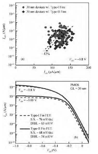
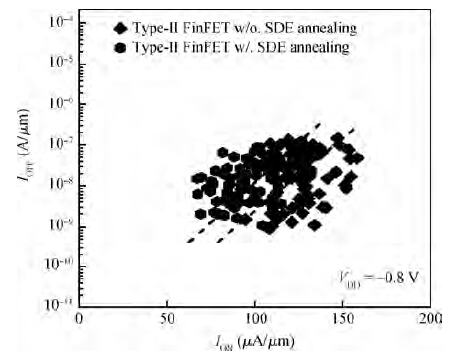
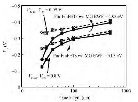
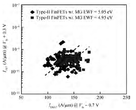
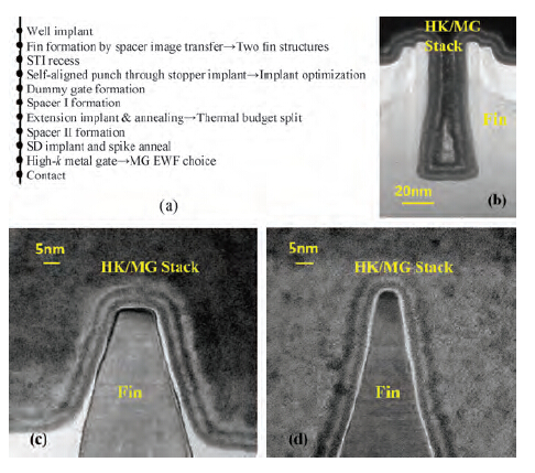
Sub-20 nm node bulk FinFET PMOS devices with an all-last high-k/metal gate (HK/MG) process are fabricated and the influence of a series of device parameters on the device scaling is investigated. The high and thin Fin structure with a tapered sidewall shows better performance than the normal Fin structure. The punch through stop layer (PTSL) and source drain extension (SDE) doping profiles are carefully optimized. The device without SDE annealing shows a larger drive current than that with SDE annealing due to better Si crystal regrowth in the amorphous Fin structure after source/drain implantation. The band-edged MG has a better short channel effect immunity, but the lower effective work function (EWF) MG shows a larger driveability. A tradeoff choice for different EWF MGs should be carefully designed for the device's scaling. -
References
[1] [2] [3] [4] [5] [6] [7] [8] -
Proportional views


 DownLoad:
